Preliminary Technical Data
FEATURES
®
Blackfin Embedded Processor ADSP-BF512/BF514/BF516/BF518(F)
PERIPHERALS
IEEE 802.3-compliant 10/100 Ethernet MAC with IEEE 1588 support (ADSP-BF518 only) Parallel peripheral interface (PPI), supporting ITU-R 656 video data formats 2 dual-channel, full-duplex synchronous serial ports (SPORTs), supporting 8 stereo I2S channels 12 peripheral DMAs, 2 mastered by the Ethernet MAC 2 memory-to-memory DMAs with external request lines Event handler with 56 interrupt inputs 2 serial peripheral interfaces (SPI) Removable storage interface (RSI) controller for MMC, SD, SDIO, and CE-ATA 2 UARTs with IrDA® support Two-wire interface (TWI) controller Eight 32-bit timers/counters with PWM support Three-phase 16-bit center-based PWM unit 32-bit general-purpose counter Real-time clock (RTC) and watchdog timer 32-bit core timer 40 general-purpose I/Os (GPIOs) Debug/JTAG interface On-chip PLL capable of 0.5 to 64 frequency multiplication
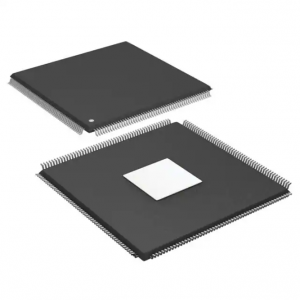
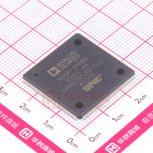
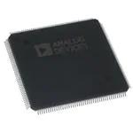
Up to 400 MHz high-performance Blackfin processor Two 16-bit MACs, two 40-bit ALUs, four 8-bit video ALUs, 40-bit shifter RISC-like register and instruction model for ease of programming and compiler-friendly support Advanced debug, trace, and performance monitoring Wide range of operating voltages. See Operating Conditions on Page 23 168-ball CSP_BGA 176-lead LQFP with exposed pad
MEMORY
116K bytes of on-chip memory External memory controller with glueless support for SDRAM and asynchronous 8-bit and 16-bit memories Optional 4 Mbit on-chip SPI flash with boot option Flexible booting options from internal SPI flash, OTP memory, external SPI/parallel memories, or from SPI/UART host devices Code security with LockboxTM secure technology One-time-programmable (OTP) memory Memory management unit providing memory protection
RTC
OTP
WATCHDOG TIMER
PERIPHERAL ACCESS BUS COUNTER
JTAG TEST AND EMULATION
3-PHASE PWM TIMER7–0
B
L1 INSTRUCTION MEMORY L1 DATA MEMORY 16 EXTERNAL ACCESS BUS EXTERNAL PORT FLASH, SDRAM CONTROL
INTERRUPT CONTROLLER
TWI SPORT1-0 RSI (SDIO) PORTS
DMA CONTROLLER DMA EXTERNAL BUS BOOT ROM 4 Mbit SPI Flash (See Table 1)
PPI UART1–0
DMA CORE BUS
EMAC SPI1 SPI0
Blackfin and the Blackfin logo are registered trademarks of Analog Devices, Inc.
Rev. PrE
Information furnished by Analog Devices is believed to be accurate and reliable. However, no responsibility is assumed by Analog Devices for its use, nor for any infringements of patents or other rights of third parties that may result from its use. Specifications subject to change without notice. No license is granted by implication or otherwise under any patent or patent rights of Analog Devices. Trademarks and registered trademarks are the property of their respective owners.
One Technology Way, P.O. Box 9106, Norwood, MA 02062-9106 U.S.A. Tel: 781.329.4700 www.analog.com Fax: 781.461.3113 © 2009 Analog Devices, Inc. All rights reserved.
�ADSP-BF512/BF514/BF516/BF518(F)
TABLE OF CONTENTS
General Description ................................................. 3 Portable Low-Power Architecture ............................. 3 System Integration ................................................ 3 Processor Peripherals ............................................. 3 Blackfin Processor Core .......................................... 3 Memory Architecture ............................................ 5 DMA Controllers .................................................. 9 Real-Time Clock ................................................... 9 Watchdog Timer ................................................ 10 Timers ............................................................. 10 3-phase PWM .................................................... 10 General-Purpose (GP) Counter .............................. 11 Serial Ports ........................................................ 11 Serial Peripheral Interface (SPI) Ports ...................... 11 UART Ports ...................................................... 11 TWI Controller Interface ...................................... 12 RSI Interface ...................................................... 12 10/100 Ethernet MAC .......................................... 12 IEEE 1588 Support .............................................. 13 Ports ................................................................ 13 Parallel Peripheral Interface (PPI) ........................... 14 Code Security with Lockbox Secure Technology ......... 14 Dynamic Power Management ................................ 14 Voltage Regulation Interface .................................. 16 Clock Signals ..................................................... 16
Preliminary Technical Data
Booting Modes ................................................... 17 Instruction Set Description .................................... 18 Development Tools .............................................. 18 Designing an Emulator-Compatible Processor Board (Target) ................................... 19 Related Documents .............................................. 19 Lockbox Secure Technology Disclaimer .................... 19 Signal Descriptions ................................................. 20 Specifications ........................................................ 23 Operating Conditions ........................................... 23 Electrical Characteristics ....................................... 25 Absolute Maximum Ratings ................................... 26 Package Information ............................................ 26 ESD Sensitivity ................................................... 26 Timing Specifications ........................................... 27 Output Drive Currents ......................................... 49 Power Dissipation ............................................... 51 Test Conditions .................................................. 51 Thermal Characteristics ........................................ 54 176-Lead LQFP Lead Assignment ............................... 55 168-Ball CSP_BGA Ball assignment ............................ 57 Outline Dimensions ................................................ 60 Surface Mount Design .......................................... 61 Ordering Guide ..................................................... 62
REVISION HISTORY
03/09—Revision PrE: Numerous small clarifications and corrections throughout document. Updated 176-lead LQFP package outline, clarifying location of exposed pad on bottom of package........................ Page 60
Rev. PrE |
Page 2 of 62 |
March 2009
�Preliminary Technical Data GENERAL DESCRIPTION
The ADSP-BF512/BF514/BF516/BF518(F) processors are members of the Blackfin family of products, incorporating the Analog Devices/Intel Micro Signal Architecture (MSA). Blackfin processors combine a dual-MAC state-of-the-art signal processing engine, the advantages of a clean, orthogonal RISClike microprocessor instruction set, and single-instruction, multiple-data (SIMD) multimedia capabilities into a single instruction-set architecture. The processors are completely code compatible with other Blackfin processors. Table 1. Processor Comparison
ADSP-BF512F ADSP-BF514F ADSP-BF516F ADSP-BF518F ADSP-BF512 ADSP-BF514 ADSP-BF516 ADSP-BF518
ADSP-BF512/BF514/BF516/BF518(F)
PORTABLE LOW-POWER ARCHITECTURE
Blackfin processors provide world-class power management and performance. They are produced with a low power and low voltage design methodology and feature on-chip dynamic power management, which is the ability to vary both the voltage and frequency of operation to significantly lower overall power consumption. This capability can result in a substantial reduction in power consumption, compared with just varying the frequency of operation. This allows longer battery life for portable appliances.
SYSTEM INTEGRATION
The ADSP-BF512/BF514/BF516/BF518(F) processors are highly integrated system-on-a-chip solutions for the next generation of embedded network connected applications. By combining industry-standard interfaces with a high performance signal processing core, cost-effective applications can be developed quickly, without the need for costly external components. The system peripherals include an IEEE-compliant 802.3 10/100 Ethernet MAC with IEEE-1588 support (ADSPBF518/ADSP-BF518F only), an RSI controller, a TWI controller, two UART ports, two SPI ports, two serial ports (SPORTs), nine general purpose 32-bit timers (eight with PWM capability), three-phase PWM for motor control, a real-time clock, a watchdog timer, and a parallel peripheral interface (PPI).
Feature IEEE-1588 Ethernet MAC RSI TWI SPORTs UARTs SPIs GP Timers Watchdog Timers RTC PPI Internal 4 Mbit SPI flash Rotary Counter 3-phase PWM Pairs GPIOs L1 Instruction SRAM L1 Instruction SRAM/Cache L1 Data SRAM L1 Data SRAM/Cache L1 Scratchpad L3 Boot ROM Maximum Speed Grade Package Options Memory (bytes)
– – – 1 2 2 2 8 1 1 1 – 1 3 40
– – – 1 2 2 2 8 1 1 1 1 1 3 40
– – 1 1 2 2 2 8 1 1 1 – 1 3 40
–– –1 11 11 22 22 22 88 11 11 11 1– 11 33 40 40 32K 16K
– 1 1 1 2 2 2 8 1 1 1 1 1 3 40
1 1 1 1 2 2 2 8 1 1 1 – 1 3 40
1 1 1 1 2 2 2 8 1 1 1 1 1 3 40
PROCESSOR PERIPHERALS
The ADSP-BF512/BF514/BF516/BF518(F) processors contain a rich set of peripherals connected to the core via several high bandwidth buses, providing flexibility in system configuration as well as excellent overall system performance (see Figure 1 on Page 4). The processors contain dedicated network communication modules and high speed serial and parallel ports, an interrupt controller for flexible management of interrupts from the on-chip peripherals or external sources, and power management control functions to tailor the performance and power characteristics of the processor and system to many application scenarios. All of the peripherals, except for the general-purpose I/O, rotary counter, TWI, three-phase PWM, real-time clock, and timers, are supported by a flexible DMA structure. There are also separate memory DMA channels dedicated to data transfers between the processor's various memory spaces, including external SDRAM and asynchronous memory. Multiple on-chip buses provide enough bandwidth to keep the processor core running along with activity on all of the on-chip and external peripherals.
32K 32K 4K 32K 400 MHz 176-Lead LQFP 168-Ball CSP_BGA
By integrating a rich set of industry-leading system peripherals and memory, Blackfin processors are the platform of choice for next-generation applications that require RISC-like programmability, multimedia support, and leading-edge signal processing in one integrated package.
BLACKFIN PROCESSOR CORE
As shown in Figure 1 on Page 4, the Blackfin processor core contains two 16-bit multipliers, two 40-bit accumulators, two 40-bit ALUs, four video ALUs, and a 40-bit shifter. The computation units process 8-, 16-, or 32-bit data from the register file.
Rev. PrE |
Page 3 of 62 |
March 2009
�ADSP-BF512/BF514/BF516/BF518(F)
The compute register file contains eight 32-bit registers. When performing compute operations on 16-bit operand data, the register file operates as 16 independent 16-bit registers. All operands for compute operations come from the multiported register file and instruction constant fields.
ADDRESS ARITHMETIC UNIT
Preliminary Technical Data
I3 I2 I1 I0 DA1 DA0 TO MEMORY 32 32
L3 L2 L1 L0
B3 B2 B1 B0
M3 M2 M1 M0 DAG1 DAG0
SP FP P5 P4 P3 P2 P1 P0
32 RAB
32 PREG
SD LD1 LD0
32 32 32
32 32
ASTAT
SEQUENCER R7.H R6.H R5.H R4.H R3.H R2.H R1.H R0.H R7.L R6.L R5.L R4.L R3.L R2.L R1.L R0.L BARREL SHIFTER 16 8 8 8 16 8 DECODE ALIGN
40 40 40
40
LOOP BUFFER
A0
A1
CONTROL UNIT
32
32 DATA ARITHMETIC UNIT
Figure 1. Blackfin Processor Core
Each MAC can perform a 16-bit by 16-bit multiply in each cycle, accumulating the results into the 40-bit accumulators. Signed and unsigned formats, rounding, and saturation are supported. The ALUs perform a traditional set of arithmetic and logical operations on 16-bit or 32-bit data. In addition, many special instructions are included to accelerate various signal processing tasks. These include bit operations such as field extract and population count, modulo 232 multiply, divide primitives, saturation and rounding, and sign/exponent detection. The set of video instructions include byte alignment and packing operations, 16-bit and 8-bit adds with clipping, 8-bit average operations, and 8-bit subtract/absolute value/accumulate (SAA) operations. Also provided are the compare/select and vector search instructions. For certain instructions, two 16-bit ALU operations can be performed simultaneously on register pairs (a 16-bit high half and 16-bit low half of a compute register). If the second ALU is used, quad 16-bit operations are possible.
Rev. PrE |
The 40-bit shifter can perform shifts and rotates and is used to support normalization, field extract, and field deposit instructions. The program sequencer controls the flow of instruction execution, including instruction alignment and decoding. For program flow control, the sequencer supports PC relative and indirect conditional jumps (with static branch prediction), and subroutine calls. Hardware is provided to support zero-overhead looping. The architecture is fully interlocked, meaning that the programmer need not manage the pipeline when executing instructions with data dependencies. The address arithmetic unit provides two addresses for simultaneous dual fetches from memory. It contains a multiported register file consisting of four sets of 32-bit index, modify, length, and base registers (for circular buffering), and eight additional 32-bit pointer registers (for C-style indexed stack manipulation).
Page 4 of 62 |
March 2009
�Preliminary Technical Data
Blackfin processors support a modified Harvard architecture in combination with a hierarchical memory structure. Level 1 (L1) memories are those that typically operate at the full processor speed with little or no latency. At the L1 level, the instruction memory holds instructions only. The two data memories hold data, and a dedicated scratchpad data memory stores stack and local variable information. In addition, multiple L1 memory blocks are provided, offering a configurable mix of SRAM and cache. The memory management unit (MMU) provides memory protection for individual tasks that may be operating on the core and can protect system registers from unintended access. The architecture provides three modes of operation: user mode, supervisor mode, and emulation mode. User mode has restricted access to certain system resources, thus providing a protected software environment, while supervisor mode has unrestricted access to the system and core resources. The Blackfin processor instruction set has been optimized so that 16-bit opcodes represent the most frequently used instructions, resulting in excellent compiled code density. Complex DSP instructions are encoded into 32-bit opcodes, representing fully featured multifunction instructions. Blackfin processors support a limited multi-issue capability, where a 32-bit instruction can be issued in parallel with two 16-bit instructions, allowing the programmer to use many of the core resources in a single instruction cycle. The Blackfin processor assembly language uses an algebraic syntax for ease of coding and readability. The architecture has been optimized for use in conjunction with the C/C++ compiler, resulting in fast and efficient software implementations.
ADSP-BF512/BF514/BF516/BF518(F)
0xFFFF FFFF CORE MMR REGISTERS (2M BYTES) 0xFFE0 0000 SYSTEM MMR REGISTERS (2M BYTES) 0xFFC0 0000 RESERVED 0xFFB0 1000 SCRATCHPAD SRAM (4K BYTES) 0xFFB0 0000 RESERVED 0xFFA1 4000 INSTRUCTION BANK C SRAM/CACHE (16K BYTES) 0xFFA1 0000 RESERVED 0xFFA0 8000 INSTRUCTION BANK B SRAM (16K BYTES) 0xFFA0 4000 INSTRUCTION BANK A SRAM (16K BYTES) 0xFFA0 0000 RESERVED 0xFF90 8000 DATA BANK B SRAM / CACHE (16K BYTES) 0xFF90 4000 DATA BANK B SRAM (16K BYTES) 0xFF90 0000 RESERVED 0xFF80 8000 DATA BANK A SRAM / CACHE (16K BYTES) 0xFF80 4000 DATA BANK A SRAM (16K BYTES) 0xFF80 0000 RESERVED 0xEF00 8000 BOOT ROM (32K BYTES) RESERVED 0x2040 0000 ASYNC MEMORY BANK 3 (1M BYTES) 0x2030 0000 ASYNC MEMORY BANK 2 (1M BYTES) 0x2020 0000 ASYNC MEMORY BANK 1 (1M BYTES) 0x2010 0000 ASYNC MEMORY BANK 0 (1M BYTES) 0x2000 0000 0x08 00 0000 0x0000 0000 RESERVED SDRAM MEMORY (16M BYTES - 128M BYTES)
EXTERNAL MEMORY MAP INTERNAL MEMORY MAP
0xEF00 0000
MEMORY ARCHITECTURE
The ADSP-BF512/BF514/BF516/BF518(F) processors view memory as a single unified 4G byte address space, using 32-bit addresses. All resources, including internal memory, external memory, and I/O control registers, occupy separate sections of this common address space. The memory portions of this address space are arranged in a hierarchical structure to provide a good cost/performance balance of some very fast, low-latency on-chip memory as cache or SRAM, and larger, lower-cost and performance off-chip memory systems. See Figure 2. The on-chip L1 memory system is the highest-performance memory available to the Blackfin processor. The off-chip memory system, accessed through the external bus interface unit (EBIU), provides expansion with SDRAM, flash memory, and SRAM, optionally accessing up to 132M bytes of physical memory. The memory DMA controller provides high-bandwidth datamovement capability. It can perform block transfers of code or data between the internal memory and the external memory spaces.
Figure 2. ADSP-BF512/BF514/BF516/BF518(F) Internal/External Memory Map
The first block is the L1 instruction memory, consisting of 48K bytes SRAM, of which 16K bytes can be configured as a four-way set-associative cache. This memory is accessed at full processor speed. The second on-chip memory block is the L1 data memory, consisting of up to two banks of up to 32K bytes each. Each memory bank is configurable, offering both cache and SRAM functionality. This memory block is accessed at full processor speed. The third memory block is a 4K byte scratchpad SRAM which runs at the same speed as the L1 memories, but is only accessible as data SRAM and cannot be configured as cache memory.
External (Off-Chip) Memory
External memory is accessed via the EBIU. This 16-bit interface provides a glueless connection to a bank of synchronous DRAM (SDRAM) as well as up to four banks of asynchronous memory devices including flash, EPROM, ROM, SRAM, and memory mapped I/O devices. The SDRAM controller can be programmed to interface to up to 128M bytes of SDRAM. A separate row can be open for each SDRAM internal bank and the SDRAM controller supports up to four internal SDRAM banks, improving overall performance.
Internal (On-Chip) Memory
The ADSP-BF512/BF514/BF516/BF518(F) processors have three blocks of on-chip memory providing high-bandwidth access to the core.
Rev. PrE |
Page 5 of 62 |
March 2009
�ADSP-BF512/BF514/BF516/BF518(F)
The asynchronous memory controller can be programmed to control up to four banks of devices with very flexible timing parameters for a wide variety of devices. Each bank occupies a 1M byte segment regardless of the size of the devices used, so that these banks are only contiguous if each is fully populated with 1M byte of memory.
Preliminary Technical Data
Booting
The processors contain a small on-chip boot kernel, which configures the appropriate peripheral for booting. If the processors are configured to boot from boot ROM memory space, the processor starts executing from the on-chip boot ROM. For more information, see Booting Modes on Page 17.
Flash Memory
The ADSP-BF512F/ADSP-BF514F/ADSP-BF516F/ ADSP-BF518F processors contain a SPI flash memory within the package of the processor and connected to SPI0. The SPI flash memory has a 4M bit capacity and 1.8V (nominal) operating voltage. The program/erase endurance is 100,000 cycles per block, and this memory has greater than 100 years data retention capability. Also included are support for software write protection and support for fast erase and byte-program. The processors internally connect to the flash memory die with the MOSI, MISO, SPISSEL, and SPI_CLK signals similar to an external SPI flash. To further provide a secure processing environment, these internally connected signals are not exposed outside of the package. For this reason, programming the ADSP-BF51xF flash memory is performed by running code on the processor. It cannot be programmed from external signals and data transfers between the SPI flash and the processor cannot be probed externally.
Event Handling
The event controller handles all asynchronous and synchronous events to the processor. The processors provide event handling that supports both nesting and prioritization. Nesting allows multiple event service routines to be active simultaneously. Prioritization ensures that servicing of a higher-priority event takes precedence over servicing of a lower-priority event. The controller provides support for five different types of events: • Emulation – An emulation event causes the processor to enter emulation mode, allowing command and control of the processor through the JTAG interface. • Reset – This event resets the processor. • Nonmaskable Interrupt (NMI) – The NMI event can be generated by the software watchdog timer or by the NMI input signal to the processor. The NMI event is frequently used as a power-down indicator to initiate an orderly shutdown of the system. • Exceptions – Events that occur synchronously to program flow; that is, the exception is taken before the instruction is allowed to complete. Conditions such as data alignment violations and undefined instructions cause exceptions. • Interrupts – Events that occur asynchronously to program flow. They are caused by input signals, timers, and other peripherals, as well as by an explicit software instruction. Each event type has an associated register to hold the return address and an associated return-from-event instruction. When an event is triggered, the state of the processor is saved on the supervisor stack. The event controller consists of two stages, the core event controller (CEC) and the system interrupt controller (SIC). The core event controller works with the system interrupt controller to prioritize and control all system events. Conceptually, interrupts from the peripherals enter into the SIC, and are then routed directly into the general-purpose interrupts of the CEC.
One-Time Programmable Memory
The processors have 64K bits of one-time programmable nonvolatile memory that can be programmed by the developer only one time. It includes the array and logic to support read access and programming. Additionally, its pages can be write protected. OTP enables developers to store both public and private data on-chip. In addition to storing public and private key data for applications requiring security, it also allows developers to store completely user-definable data such as customer ID, product ID, and MAC address. Hence generic parts can be shipped which are then programmed and protected by the developer within this non-volatile memory.
I/O Memory Space
The processors do not define a separate I/O space. All resources are mapped through the flat 32-bit address space. On-chip I/O devices have their control registers mapped into memorymapped registers (MMRs) at addresses near the top of the 4G byte address space. These are separated into two smaller blocks, one which contains the control MMRs for all core functions, and the other which contains the registers needed for setup and control of the on-chip peripherals outside of the core. The MMRs are accessible only in supervisor mode and appear as reserved space to on-chip peripherals.
Core Event Controller (CEC)
The CEC supports nine general-purpose interrupts (IVG15–7), in addition to the dedicated interrupt and exception events. Of these general-purpose interrupts, the two lowest-priority interrupts (IVG15–14) are recommended to be reserved for software interrupt handlers, leaving seven prioritized interrupt inputs to support the peripherals of the processors. Table 2 describes the inputs to the CEC, identifies their names in the event vector table (EVT), and lists their priorities.
Rev. PrE |
Page 6 of 62 |
March 2009
�Preliminary Technical Data
Table 2. Core Event Controller (CEC)
Priority (0 is Highest) Event Class 0 1 2 3 4 5 6 7 8 9 10 11 12 13 14 15 Emulation/Test Control Reset Nonmaskable Interrupt Exception Reserved Hardware Error Core Timer General-Purpose Interrupt 7 General-Purpose Interrupt 8 General-Purpose Interrupt 9 General-Purpose Interrupt 10 General-Purpose Interrupt 11 General-Purpose Interrupt 12 General-Purpose Interrupt 13 General-Purpose Interrupt 14 General-Purpose Interrupt 15 EVT Entry EMU RST NMI EVX — IVHW IVTMR IVG7 IVG8 IVG9 IVG10 IVG11 IVG12 IVG13 IVG14 IVG15
ADSP-BF512/BF514/BF516/BF518(F)
ing the appropriate values into the interrupt assignment registers (SIC_IARx). Table 3 describes the inputs into the SIC and the default mappings into the CEC.
Event Control
The ADSP-BF512/BF514/BF516/BF518(F) processors provide a very flexible mechanism to control the processing of events. In the CEC, three registers are used to coordinate and control events. Each register is 16 bits wide. • CEC interrupt latch register (ILAT) – Indicates when events have been latched. The appropriate bit is set when the processor has latched the event and cleared when the event has been accepted into the system. This register is updated automatically by the controller, but it may be written only when its corresponding IMASK bit is cleared. • CEC interrupt mask register (IMASK) – Controls the masking and unmasking of individual events. When a bit is set in the IMASK register, that event is unmasked and is processed by the CEC when asserted. A cleared bit in the IMASK register masks the event, preventing the processor from servicing the event even though the event may be latched in the ILAT register. This register may be read or written while in supervisor mode. (Note that general-purpose interrupts can be globally enabled and disabled with the STI and CLI instructions, respectively.) • CEC interrupt pending register (IPEND) – The IPEND register keeps track of all nested events. A set bit in the IPEND register indicates the event is currently active or nested at some level. This register is updated automatically by the controller but may be read while in supervisor mode.
System Interrupt Controller (SIC)
The system interrupt controller provides the mapping and routing of events from the many peripheral interrupt sources to the prioritized general-purpose interrupt inputs of the CEC. Although the processors provide a default mapping, the user can alter the mappings and priorities of interrupt events by writTable 3. Peripheral Interrupt Assignment
Peripheral Interrupt Event PLL Wakeup Interrupt DMA Error 0 (generic) DMAR0 Block Interrupt DMAR1 Block Interrupt DMAR0 Overflow Error DMAR1 Overflow Error PPI Error MAC Status SPORT0 Status SPORT1 Status PTP Error Interrupt Reserved UART0 Status UART1 Status RTC DMA 0 Channel (PPI) DMA 3 Channel (SPORT0 RX) General Purpose Interrupt (at Reset) IVG7 IVG7 IVG7 IVG7 IVG7 IVG7 IVG7 IVG7 IVG7 IVG7 IVG7 IVG7 IVG7 IVG7 IVG8 IVG8 IVG9
Peripheral Interrupt ID 0 1 2 3 4 5 6 7 8 9 10 11 12 13 14 15 16
Default Core Interrupt ID 0 0 0 0 0 0 0 0 0 0 0 0 0 0 1 1 2
SIC Registers IAR0 IAR0 IAR0 IAR0 IAR0 IAR0 IAR0 IAR0 IAR1 IAR1 IAR1 IAR1 IAR1 IAR1 IAR1 IAR1 IAR2 IMASK0 and ISR0 IMASK0 and ISR0 IMASK0 and ISR0 IMASK0 and ISR0 IMASK0 and ISR0 IMASK0 and ISR0 IMASK0 and ISR0 IMASK0 and ISR0 IMASK0 and ISR0 IMASK0 and ISR0 IMASK0 and ISR0 IMASK0 and ISR0 IMASK0 and ISR0 IMASK0 and ISR0 IMASK0 and ISR0 IMASK0 and ISR0 IMASK0 and ISR0
Rev. PrE |
Page 7 of 62 |
March 2009
�ADSP-BF512/BF514/BF516/BF518(F)
Table 3. Peripheral Interrupt Assignment (Continued)
Peripheral Interrupt Event DMA 4 Channel (SPORT0 TX/RSI) DMA 5 Channel (SPORT1 RX/SPI1) DMA 6 Channel (SPORT1 TX) TWI DMA 7 Channel (SPI0) DMA8 Channel (UART0 RX) DMA9 Channel (UART0 TX) DMA10 Channel (UART1 Rx) DMA11 Channel (UART1 Tx) OTP Memory Interrupt GP Counter DMA1 Channel (MAC RX) Port H Interrupt A DMA2 Channel (MAC TX) Port H Interrupt B Timer 0 Timer 1 Timer 2 Timer 3 Timer 4 Timer 5 Timer 6 Timer 7 Port G Interrupt A Port G Interrupt B MDMA Stream 0 MDMA Stream 1 Software Watchdog Timer Port F Interrupt A Port F Interrupt B SPI0 Status SPI1 Status Reserved Reserved RSI Interrupt0 RSI Interrupt1 PWM Trip Interrupt PWM Sync Interrupt PTP Status Interrupt General Purpose Interrupt (at Reset) IVG9 IVG9 IVG9 IVG10 IVG10 IVG10 IVG10 IVG10 IVG10 IVG11 IVG11 IVG11 IVG11 IVG11 IVG11 IVG12 IVG12 IVG12 IVG12 IVG12 IVG12 IVG12 IVG12 IVG12 IVG12 IVG13 IVG13 IVG13 IVG13 IVG13 IVG7 IVG7 IVG7 IVG7 IVG10 IVG10 IVG10 IVG10 IVG10 Peripheral Interrupt ID 17 18 19 20 21 22 23 24 25 26 27 28 29 30 31 32 33 34 35 36 37 38 39 40 41 42 43 44 45 46 47 48 49 50 51 52 53 54 55
Preliminary Technical Data
Default Core Interrupt ID 2 2 2 3 3 3 3 3 3 4 4 4 4 4 4 5 5 5 5 5 5 5 5 5 5 6 6 6 6 6 0 0 0 0 3 3 3 3 3
SIC Registers IAR2 IAR2 IAR2 IAR2 IAR2 IAR2 IAR2 IAR3 IAR3 IAR3 IAR3 IAR3 IAR3 IAR3 IAR3 IAR4 IAR4 IAR4 IAR4 IAR4 IAR4 IAR4 IAR4 IAR5 IAR5 IAR5 IAR5 IAR5 IAR5 IAR5 IAR5 IAR6 IAR6 IAR6 IAR6 IAR6 IAR6 IAR6 IAR6 IMASK0 and ISR0 IMASK0 and ISR0 IMASK0 and ISR0 IMASK0 and ISR0 IMASK0 and ISR0 IMASK0 and ISR0 IMASK0 and ISR0 IMASK0 and ISR0 IMASK0 and ISR0 IMASK0 and ISR0 IMASK0 and ISR0 IMASK0 and ISR0 IMASK0 and ISR0 IMASK0 and ISR0 IMASK0 and ISR0 IMASK1 and ISR1 IMASK1 and ISR1 IMASK1 and ISR1 IMASK1 and ISR1 IMASK1 and ISR1 IMASK1 and ISR1 IMASK1 and ISR1 IMASK1 and ISR1 IMASK1 and ISR1 IMASK1 and ISR1 IMASK1 and ISR1 IMASK1 and ISR1 IMASK1 and ISR1 IMASK1 and ISR1 IMASK1 and ISR1 IMASK1 and ISR1 IMASK1 and ISR1 IMASK1 and ISR1 IMASK1 and ISR1 IMASK1 and ISR1 IMASK1 and ISR1 IMASK1 and ISR1 IMASK1 and ISR1 IMASK1 and ISR1
Rev. PrE |
Page 8 of 62 |
March 2009
�Preliminary Technical Data
The SIC allows further control of event processing by providing three pairs of 32-bit interrupt control and status registers. Each register contains a bit corresponding to each of the peripheral interrupt events shown in Table 3 on Page 7. • SIC interrupt mask registers (SIC_IMASKx) – Control the masking and unmasking of each peripheral interrupt event. When a bit is set in these registers, that peripheral event is unmasked and is processed by the system when asserted. A cleared bit in the register masks the peripheral event, preventing the processor from servicing the event. • SIC interrupt status registers (SIC_ISRx) – As multiple peripherals can be mapped to a single event, these registers allow the software to determine which peripheral event source triggered the interrupt. A set bit indicates the peripheral is asserting the interrupt, and a cleared bit indicates the peripheral is not asserting the event. • SIC interrupt wakeup enable registers (SIC_IWRx) – By enabling the corresponding bit in these registers, a peripheral can be configured to wake up the processor, should the core be idled when the event is generated. For more information see Dynamic Power Management on Page 14. Because multiple interrupt sources can map to a single generalpurpose interrupt, multiple pulse assertions can occur simultaneously, before or during interrupt processing for an interrupt event already detected on this interrupt input. The IPEND register contents are monitored by the SIC as the interrupt acknowledgement. The appropriate ILAT register bit is set when an interrupt rising edge is detected (detection requires two core clock cycles). The bit is cleared when the respective IPEND register bit is set. The IPEND bit indicates that the event has entered into the processor pipeline. At this point the CEC recognizes and queues the next rising edge event on the corresponding event input. The minimum latency from the rising edge transition of the generalpurpose interrupt to the IPEND output asserted is three core clock cycles; however, the latency can be much higher, depending on the activity within and the state of the processor.
ADSP-BF512/BF514/BF516/BF518(F)
The 2-D DMA capability supports arbitrary row and column sizes up to 64K elements by 64K elements, and arbitrary row and column step sizes up to ±32K elements. Furthermore, the column step size can be less than the row step size, allowing implementation of interleaved data streams. This feature is especially useful in video applications where data can be deinterleaved on the fly. Examples of DMA types supported by the DMA controller include: • A single, linear buffer that stops upon completion • A circular, auto-refreshing buffer that interrupts on each full or fractionally full buffer • 1-D or 2-D DMA using a linked list of descriptors • 2-D DMA using an array of descriptors, specifying only the base DMA address within a common page In addition to the dedicated peripheral DMA channels, there are two memory DMA channels that transfer data between the various memories of the processor system. This enables transfers of blocks of data between any of the memories—including external SDRAM, ROM, SRAM, and flash memory—with minimal processor intervention. Memory DMA transfers can be controlled by a very flexible descriptor-based methodology or by a standard register-based autobuffer mechanism. The processors also have an external DMA controller capability via dual external DMA request signals when used in conjunction with the external bus interface unit (EBIU). This functionality can be used when a high speed interface is required for external FIFOs and high bandwidth communications peripherals. It allows control of the number of data transfers for memory DMA. The number of transfers per edge is programmable. This feature can be programmed to allow memory DMA to have an increased priority on the external bus relative to the core.
REAL-TIME CLOCK
The real-time clock (RTC) provides a robust set of digital watch features, including current time, stopwatch, and alarm. The RTC is clocked by a 32.768 kHz crystal external to the processors. The RTC peripheral has a dedicated power supply so that it can remain powered up and clocked even when the rest of the processor is in a low-power state. The RTC provides several programmable interrupt options, including interrupt per second, minute, hour, or day clock ticks, interrupt on programmable stopwatch countdown, or interrupt at a programmed alarm time. The 32.768 kHz input clock frequency is divided down to a 1 Hz signal by a prescaler. The counter function of the timer consists of four counters: a 60-second counter, a 60-minute counter, a 24-hour counter, and an 32,768-day counter. When enabled, the alarm function generates an interrupt when the output of the timer matches the programmed value in the alarm control register. There are two alarms: The first alarm is for a time of day. The second alarm is for a day and time of that day.
DMA CONTROLLERS
The ADSP-BF512/BF514/BF516/BF518(F) processors have multiple, independent DMA channels that support automated data transfers with minimal overhead for the processor core. DMA transfers can occur between the processor's internal memories and any of its DMA-capable peripherals. Additionally, DMA transfers can be accomplished between any of the DMA-capable peripherals and external devices connected to the external memory interfaces, including the SDRAM controller and the asynchronous memory controller. DMA-capable peripherals include the Ethernet MAC, RSI, SPORTs, SPIs, UARTs, and PPI. Each individual DMA-capable peripheral has at least one dedicated DMA channel. The processors’ DMA controller supports both one-dimensional (1-D) and two-dimensional (2-D) DMA transfers. DMA transfer initialization can be implemented from registers or from sets of parameters called descriptor blocks.
Rev. PrE |
Page 9 of 62 |
March 2009
�ADSP-BF512/BF514/BF516/BF518(F)
The stopwatch function counts down from a programmed value, with one-second resolution. When the stopwatch is enabled and the counter underflows, an interrupt is generated. Like the other peripherals, the RTC can wake up the processor from sleep mode upon generation of any RTC wakeup event. Additionally, an RTC wakeup event can wake up the processor from deep sleep mode or cause a transition from the hibernate state. Connect RTC signals RTXI and RTXO with external components as shown in Figure 3.
RTXI R1 RTXO
Preliminary Technical Data
pulse width modulator (PWM) or timer output, as an input to clock the timer, or as a mechanism for measuring pulse widths and periods of external events. These timers can be synchronized to an external clock input to the several other associated PF signals, an external clock input to the PPI_CLK input signal, or to the internal SCLK. The timer units can be used in conjunction with the two UARTs to measure the width of the pulses in the data stream to provide a software auto-baud detect function for the respective serial channels. The timers can generate interrupts to the processor core providing periodic events for synchronization, either to the system clock or to a count of external signals. In addition to the eight general-purpose programmable timers, a ninth timer is also provided. This extra timer is clocked by the internal processor clock and is typically used as a system tick clock for generation of operating system periodic interrupts.
X1 C1 C2
3-PHASE PWM
Features of the 3-phase PWM generation unit are:
SUGGES TED COMPONENTS: X1 = ECL IPTEK EC38J (THROUGH-HOLE PACKAGE) OR EPSON MC405 12 pF LOAD (S URFACE-MOUNT PACKAGE) C1 = 22 pF C2 = 22 pF R1 = 10 M Ω NOTE: C1 AND C2 ARE S PECIFIC TO CRY STAL SPECI FIED FOR X1. CONTACT CRY STAL MANUFACTURER FOR DETAILS. C1 AND C2 SPECIFICATIONS ASSUME BOARD TRACE CAPACITANCE OF 3 pF.
• 16-bit center-based PWM generation unit • Programmable PWM pulse width • Single/double update modes • Programmable dead time and switching frequency • Twos-complement implementation which permits smooth transition to full ON and full OFF states • Possibility to synchronize the PWM generation to an external synchronization • Special provisions for BDCM operation (crossover and output enable functions) • Wide variety of special switched reluctance (SR) operating modes • Output polarity and clock gating control • Dedicated asynchronous PWM shutdown signal The processors integrate a flexible and programmable 3-phase PWM waveform generator that can be programmed to generate the required switching patterns to drive a 3-phase voltage source inverter for ac induction (ACIM) or permanent magnet synchronous (PMSM) motor control. In addition, the PWM block contains special functions that considerably simplify the generation of the required PWM switching patterns for control of the electronically commutated motor (ECM) or brushless dc motor (BDCM). Software can enable a special mode for switched reluctance motors (SRM). The six PWM output signals consist of three high-side drive signals (PWM_AH, PWM_BH, and PWM_CH) and three low-side drive signals (PWM_AL, PWM_BL, and PWM_CL). The polarity of the generated PWM signal be set with software, so that either active HI or active LO PWM patterns can be produced. The switching frequency of the generated PWM pattern is programmable using the 16-bit PWMTM register. The PWM generator can operate in single update mode or double update
March 2009
Figure 3. External Components for RTCT
WATCHDOG TIMER
The ADSP-BF512/BF514/BF516/BF518(F) processors include a 32-bit timer that can be used to implement a software watchdog function. A software watchdog can improve system availability by forcing the processor to a known state through generation of a hardware reset, nonmaskable interrupt (NMI), or generalpurpose interrupt, if the timer expires before being reset by software. The programmer initializes the count value of the timer, enables the appropriate interrupt, then enables the timer. Thereafter, the software must reload the counter before it counts to zero from the programmed value. This protects the system from remaining in an unknown state where software, which would normally reset the timer, has stopped running due to an external noise condition or software error. If configured to generate a hardware reset, the watchdog timer resets both the core and the processor peripherals. After a reset, software can determine if the watchdog was the source of the hardware reset by interrogating a status bit in the watchdog timer control register. The timer is clocked by the system clock (SCLK), at a maximum frequency of fSCLK.
TIMERS
There are nine general-purpose programmable timer units in the ADSP-BF512/BF514/BF516/BF518(F) processors. Eight timers have an external signal that can be configured either as a
Rev. PrE |
Page 10 of 62 |
�Preliminary Technical Data
mode. In single update mode the duty cycle values are programmable only once per PWM period, so that the resultant PWM patterns are symmetrical about the midpoint of the PWM period. In the double update mode, a second updating of the PWM registers is implemented at the midpoint of the PWM period. In this mode, it is possible to produce asymmetrical PWM patterns that produce lower harmonic distortion in 3-phase PWM inverters.
ADSP-BF512/BF514/BF516/BF518(F)
• DMA operations with single-cycle overhead – Each SPORT can automatically receive and transmit multiple buffers of memory data. The processor can link or chain sequences of DMA transfers between a SPORT and memory. • Interrupts – Each transmit and receive port generates an interrupt upon completing the transfer of a data word or after transferring an entire data buffer, or buffers, through DMA. • Multichannel capability – Each SPORT supports 128 channels out of a 1024-channel window and is compatible with the H.100, H.110, MVIP-90, and HMVIP standards.
GENERAL-PURPOSE (GP) COUNTER
A 32-bit GP counter is provided that can sense 2-bit quadrature or binary codes as typically emitted by industrial drives or manual thumb wheels. The counter can also operate in generalpurpose up/down count modes. Then, count direction is either controlled by a level-sensitive input signal or by two edge detectors. A third input can provide flexible zero marker support and can alternatively be used to input the push-button signal of thumb wheels. All three signals have a programmable debouncing circuit. An internal signal forwarded to the GP timer unit enables one timer to measure the intervals between count events. Boundary registers enable auto-zero operation or simple system warning by interrupts when programmable count values are exceeded.
SERIAL PERIPHERAL INTERFACE (SPI) PORTS
The processors have two SPI-compatible ports (SPI0 and SPI1) that enable the processor to communicate with multiple SPIcompatible devices. The SPI interface uses three signals for transferring data: two data signals (master output-slave input–MOSI, and master input-slave output–MISO) and a clock signal (serial clock–SCK). An SPI chip select input signal (SPIxSS) lets other SPI devices select the processor, and multiple SPI chip select output signals let the processor select other SPI devices. The SPI select signals are reconfigured general-purpose I/O signals. Using these signals, the SPI port provides a full-duplex, synchronous serial interface, which supports both master/slave modes and multimaster environments. The SPI port baud rate and clock phase/polarities are programmable, and it has an integrated DMA channel, configurable to support transmit or receive data streams. The SPI’s DMA channel can only service unidirectional accesses at any given time. The SPI port clock rate is calculated as: f SCLK SPI Clock Rate = ----------------------------------2 × SPI_BAUD Where the 16-bit SPI_BAUD register contains a value of 2 to 65,535. During transfers, the SPI port simultaneously transmits and receives by serially shifting data in and out on its two serial data lines. The serial clock line synchronizes the shifting and sampling of data on the two serial data lines.
SERIAL PORTS
The ADSP-BF512/BF514/BF516/BF518(F) processors incorporate two dual-channel synchronous serial ports (SPORT0 and SPORT1) for serial and multiprocessor communications. The SPORTs support the following features: • I2S capable operation. • Bidirectional operation – Each SPORT has two sets of independent transmit and receive signals, enabling eight channels of I2S stereo audio. • Buffered (8-deep) transmit and receive ports – Each port has a data register for transferring data words to and from other processor components and shift registers for shifting data in and out of the data registers. • Clocking – Each transmit and receive port can either use an external serial clock or generate its own, in frequencies ranging from (fSCLK/131,070) Hz to (fSCLK/2) Hz. • Word length – Each SPORT supports serial data words from 3 to 32 bits in length, transferred most-significant-bit first or least-significant-bit first. • Framing – Each transmit and receive port can run with or without frame sync signals for each data word. Frame sync signals can be generated internally or externally, active high or low, and with either of two pulse widths and early or late frame sync. • Companding in hardware – Each SPORT can perform A-law or μ-law companding according to ITU recommendation G.711. Companding can be selected on the transmit and/or receive channel of the SPORT without additional latencies.
UART PORTS
The ADSP-BF512/BF514/BF516/BF518(F) processors provide two full-duplex universal asynchronous receiver/transmitter (UART) ports, which are fully compatible with PC-standard UARTs. Each UART port provides a simplified UART interface to other peripherals or hosts, supporting full-duplex, DMA-supported, asynchronous transfers of serial data. A UART port
Rev. PrE |
Page 11 of 62 |
March 2009
�ADSP-BF512/BF514/BF516/BF518(F)
includes support for five to eight data bits, one or two stop bits, and none, even, or odd parity. Each UART port supports two modes of operation: • PIO (programmed I/O) – The processor sends or receives data by writing or reading I/O mapped UART registers. The data is double-buffered on both transmit and receive. • DMA (direct memory access) – The DMA controller transfers both transmit and receive data. This reduces the number and frequency of interrupts required to transfer data to and from memory. The UART has two dedicated DMA channels, one for transmit and one for receive. These DMA channels have lower default priority than most DMA channels because of their relatively low service rates. Each UART port's baud rate, serial data format, error code generation and status, and interrupts are programmable: • Supporting bit rates ranging from (fSCLK/1,048,576) to (fSCLK/16) bits per second. • Supporting data formats from seven to 12 bits per frame. • Both transmit and receive operations can be configured to generate maskable interrupts to the processor. The UART port’s clock rate is calculated as: f SCLK UART Clock Rate = ---------------------------------------------16 × UART_Divisor Where the 16-bit UART_Divisor comes from the UART_DLH (most significant 8 bits) and UART_DLL (least significant 8 bits) registers. In conjunction with the general-purpose timer functions, autobaud detection is supported. The capabilities of the UARTs are further extended with support for the infrared data association (IrDA®) serial infrared physical layer link specification (SIR) protocol.
Preliminary Technical Data
RSI INTERFACE
The removable storage interface (RSI) controller acts as the host interface for multi-media cards (MMC), secure digital memory cards (SD Card), secure digital input/output cards (SDIO), and CE-ATA hard disk drives. The following list describes the main features of the RSI controller. • Support for a single MMC, SD memory, SDIO card or CEATA hard disk drive • Support for 1-bit and 4-bit SD modes • Support for 1-bit, 4-bit and 8-bit MMC modes • Support for 4-bit and 8-bit CE-ATA hard disk drives • A ten-signal external interface with clock, command, and up to eight data lines • Card detection using one of the data signals • Card interface clock generation from SCLK • SDIO interrupt and read wait features • CE-ATA command completion signal recognition and disable
10/100 ETHERNET MAC
The ADSP-BF516/BF518 processors offer the capability to directly connect to a network by way of an embedded fast Ethernet media access controller (MAC) that supports both 10-BaseT (10M bits/sec) and 100-BaseT (100M bits/sec) operation. The 10/100 Ethernet MAC peripheral on the processor is fully compliant to the IEEE 802.3-2002 standard and it provides programmable features designed to minimize supervision, bus use, or message processing by the rest of the processor system. Some standard features are: • Support of MII and RMII protocols for external PHYs • Full duplex and half duplex modes • Data framing and encapsulation: generation and detection of preamble, length padding, and FCS • Media access management (in half-duplex operation): collision and contention handling, including control of retransmission of collision frames and of back-off timing • Flow control (in full-duplex operation): generation and detection of pause frames • Station management: generation of MDC/MDIO frames for read-write access to PHY registers • SCLK operating range down to 25 MHz (active and sleep operating modes) • Internal loopback from transmit to receive Some advanced features are: • Buffered crystal output to external PHY for support of a single crystal system • Automatic checksum computation of IP header and IP payload fields of Rx frames • Independent 32-bit descriptor-driven receive and transmit DMA channels
Rev. PrE | Page 12 of 62 | March 2009
TWI CONTROLLER INTERFACE
The processors include a two wire interface (TWI) module for providing a simple exchange method of control data between multiple devices. The TWI is compatible with the widely used I2C® bus standard. The TWI module offers the capabilities of simultaneous master and slave operation, support for both 7-bit addressing and multimedia data arbitration. The TWI interface utilizes two signals for transferring clock (SCL) and data (SDA) and supports the protocol at speeds up to 400k bits/sec. The TWI interface signals are compatible with 5 V logic levels. Additionally, the processor’s TWI module is fully compatible with serial camera control bus (SCCB) functionality for easier control of various CMOS camera sensor devices.
�Preliminary Technical Data
• Frame status delivery to memory through DMA, including frame completion semaphores for efficient buffer queue management in software • Tx DMA support for separate descriptors for MAC header and payload to eliminate buffer copy operations • Convenient frame alignment modes support even 32-bit alignment of encapsulated receive or transmit IP packet data in memory after the 14-byte MAC header • Programmable Ethernet event interrupt supports any combination of: • Selected receive or transmit frame status conditions • PHY interrupt condition • Wakeup frame detected • Selected MAC management counter(s) at half-full • DMA descriptor error • 47 MAC management statistics counters with selectable clear-on-read behavior and programmable interrupts on half maximum value • Programmable receive address filters, including a 64-bin address hash table for multicast and/or unicast frames, and programmable filter modes for broadcast, multicast, unicast, control, and damaged frames • Advanced power management supporting unattended transfer of receive and transmit frames and status to/from external memory via DMA during low-power sleep mode • System wakeup from sleep operating mode upon magic packet or any of four user-definable wakeup frame filters • Support for 802.3Q tagged VLAN frames • Programmable MDC clock rate and preamble suppression • In RMII operation, seven unused signals may be configured as GPIO signals for other purposes
ADSP-BF512/BF514/BF516/BF518(F)
• Multiple input clock sources (SCLK, MII clock, external clock up to 50 MHz) • Programmable pulse per second (PPS) output • Auxiliary snapshot to time stamp external events
PORTS
Because of the rich set of peripherals, the processors group the many peripheral signals to four ports—port F, port G, port H, and port J. Most of the associated pins/balls are shared by multiple signals. The ports function as multiplexer controls.
General-Purpose I/O (GPIO)
The ADSP-BF512/BF514/BF516/BF518(F) processors have 40 bidirectional, general-purpose I/O (GPIO) signals allocated across three separate GPIO modules—PORTFIO, PORTGIO, and PORTHIO, associated with Port F, Port G, and Port H, respectively. Each GPIO-capable signal shares functionality with other peripherals via a multiplexing scheme; however, the GPIO functionality is the default state of the device upon power-up. Neither GPIO output nor input drivers are active by default. Each general-purpose port signal can be individually controlled by manipulation of the port control, status, and interrupt registers: • GPIO direction control register – Specifies the direction of each individual GPIO signal as input or output. • GPIO control and status registers – The processor employs a “write one to modify” mechanism that allows any combination of individual GPIO signals to be modified in a single instruction, without affecting the level of any other GPIO signals. Four control registers are provided. One register is written in order to set signal values, one register is written in order to clear signal values, one register is written in order to toggle signal values, and one register is written in order to specify a signal value. Reading the GPIO status register allows software to interrogate the sense of the signals. • GPIO interrupt mask registers – The two GPIO interrupt mask registers allow each individual GPIO signal to function as an interrupt to the processor. Similar to the two GPIO control registers that are used to set and clear individual signal values, one GPIO interrupt mask register sets bits to enable interrupt function, and the other GPIO interrupt mask register clears bits to disable interrupt function. GPIO signals defined as inputs can be configured to generate hardware interrupts, while output signals can be triggered by software interrupts. • GPIO interrupt sensitivity registers – The two GPIO interrupt sensitivity registers specify whether individual signals are level- or edge-sensitive and specify—if edge-sensitive— whether just the rising edge or both the rising and falling edges of the signal are significant. One register selects the type of sensitivity, and one register selects which edges are significant for edge-sensitivity.
IEEE 1588 SUPPORT
The IEEE 1588 standard is a precision clock synchronization protocol for networked measurement and control systems. The ADSP-BF518/ADSP-BF518F processors include hardware support for IEEE 1588 with an integrated precision time protocol synchronization engine (PTP_TSYNC). This engine provides hardware assisted time stamping to improve the accuracy of clock synchronization between PTP nodes. The main features of the PTP_SYNC engine are: • Support for both IEEE 1588-2002 and IEEE 1588-2008 protocol standards • Hardware assisted time stamping capable of 12.5 ns resolution • Lock adjustment • Programmable PTM message support • Dedicated interrupts • Programmable alarm
Rev. PrE |
Page 13 of 62 |
March 2009
�ADSP-BF512/BF514/BF516/BF518(F)
PARALLEL PERIPHERAL INTERFACE (PPI)
The ADSP-BF512/BF514/BF516/BF518(F) processors provide a parallel peripheral interface (PPI) that can connect directly to parallel A/D and D/A converters, ITU-R-601/656 video encoders and decoders, and other general-purpose peripherals. The PPI consists of a dedicated input clock signal, up to three frame synchronization signals, and up to 16 data signals. In ITU-R-656 modes, the PPI receives and parses a data stream of 8-bit or 10-bit data elements. On-chip decode of embedded preamble control and synchronization information is supported. Three distinct ITU-R-656 modes are supported: • Active video only mode – The PPI does not read in any data between the End of Active Video (EAV) and Start of Active Video (SAV) preamble symbols, or any data present during the vertical blanking intervals. In this mode, the control byte sequences are not stored to memory; they are filtered by the PPI. • Vertical blanking only mode – The PPI only transfers vertical blanking interval (VBI) data, as well as horizontal blanking information and control byte sequences on VBI lines. • Entire field mode – The entire incoming bitstream is read in through the PPI. This includes active video, control preamble sequences, and ancillary data that may be embedded in horizontal and vertical blanking intervals. Though not explicitly supported, ITU-R-656 output functionality can be achieved by setting up the entire frame structure (including active video, blanking, and control information) in memory and streaming the data out the PPI in a frame sync-less mode. The processor’s 2-D DMA features facilitate this transfer by allowing the static frame buffer (blanking and control codes) to be placed in memory once, and simply updating the active video information on a per-frame basis. The general-purpose modes of the PPI are intended to suit a wide variety of data capture and transmission applications. The modes are divided into four main categories, each allowing up to 16 bits of data transfer per PPI_CLK cycle: • Data receive with internally generated frame syncs • Data receive with externally generated frame syncs • Data transmit with internally generated frame syncs • Data transmit with externally generated frame syncs These modes support ADC/DAC connections, as well as video communication with hardware signalling. Many of the modes support more than one level of frame synchronization. If desired, a programmable delay can be inserted between assertion of a frame sync and reception/transmission of data.
Preliminary Technical Data
CODE SECURITY WITH LOCKBOX SECURE TECHNOLOGY
A security system consisting of a blend of hardware and software provides customers with a flexible and rich set of code security features with Lockbox secure technology. Key features include: • OTP memory • Unique chip ID • Code authentication • Secure mode of operation The security scheme is based upon the concept of authentication of digital signatures using standards-based algorithms and provides a secure processing environment in which to execute code and protect assets.
DYNAMIC POWER MANAGEMENT
The ADSP-BF512/BF514/BF516/BF518(F) processors provide four operating modes, each with a different performance/power profile. In addition, dynamic power management provides the control functions to dynamically alter the processor core supply voltage, further reducing power dissipation. When configured for a 0 volt core supply voltage, the processor enters the hibernate state. Control of clocking to each of the processor peripherals also reduces power consumption. See Table 4 for a summary of the power settings for each mode. Table 4. Power Settings
Core PLL Clock Bypassed (CCLK) System Clock (SCLK) Core Power
Mode/State PLL Full On Active Sleep Deep Sleep Hibernate
Enabled No Enabled/ Yes Disabled Enabled — Disabled — Disabled —
Enabled Enabled On Enabled Enabled On Disabled Enabled On Disabled Disabled On Disabled Disabled Off
Full-On Operating Mode—Maximum Performance
In the full-on mode, the PLL is enabled and is not bypassed, providing capability for maximum operational frequency. This is the power-up default execution state in which maximum performance can be achieved. The processor core and all enabled peripherals run at full speed.
Active Operating Mode—Moderate Power Savings
In the active mode, the PLL is enabled but bypassed. Because the PLL is bypassed, the processor’s core clock (CCLK) and system clock (SCLK) run at the input clock (CLKIN) frequency. In this mode, the CLKIN to CCLK multiplier ratio can be changed, although the changes are not realized until the full-on mode is entered. DMA access is available to appropriately configured L1 memories.
Rev. PrE |
Page 14 of 62 |
March 2009
�Preliminary Technical Data
In the active mode, it is possible to disable the PLL through the PLL control register (PLL_CTL). If disabled, the PLL must be re-enabled before transitioning to the full-on or sleep modes.
ADSP-BF512/BF514/BF516/BF518(F)
SDRAM. The SCKELOW bit in the VR_CTL register controls whether or not SDRAM operates in self-refresh mode, which allows it to retain its content while the processor is in hibernation and through the subsequent reset sequence.
Sleep Operating Mode—High Dynamic Power Savings
The sleep mode reduces dynamic power dissipation by disabling the clock to the processor core (CCLK). The PLL and system clock (SCLK), however, continue to operate in this mode. Typically an external event or RTC activity wakes up the processor. When in the sleep mode, asserting wakeup causes the processor to sense the value of the BYPASS bit in the PLL control register (PLL_CTL). If BYPASS is disabled, the processor transitions to the full on mode. If BYPASS is enabled, the processor transitions to the active mode. System DMA access to L1 memory is not supported in sleep mode.
Power Savings
As shown in Table 5, the processors support up to six different power domains, which maximizes flexibility while maintaining compliance with industry standards and conventions. By isolating the internal logic of the processor into its own power domain, separate from the RTC and other I/O, the processor can take advantage of dynamic power management without affecting the RTC or other I/O devices. There are no sequencing requirements for the various power domains, but all domains must be powered according to the appropriate Specifications table for processor Operating Conditions; even if the feature/peripheral is not used. Table 5. Power Domains
Power Domain All internal logic, except RTC, Memory, OTP RTC internal logic and crystal I/O Memory logic OTP logic Optional internal flash All other I/O VDD Range VDDINT VDDRTC VDDMEM VDDOTP VDDFLASH VDDEXT
Deep Sleep Operating Mode—Maximum Dynamic Power Savings
The deep sleep mode maximizes dynamic power savings by disabling the clocks to the processor core (CCLK) and to all synchronous peripherals (SCLK). Asynchronous peripherals, such as the RTC, may still be running but cannot access internal resources or external memory. This powered-down mode can only be exited by assertion of the reset interrupt (RESET) or by an asynchronous interrupt generated by the RTC. When in deep sleep mode, an RTC asynchronous interrupt causes the processor to transition to the Active mode. Assertion of RESET while in deep sleep mode causes the processor to transition to the full on mode.
Hibernate State—Maximum Static Power Savings
The hibernate state maximizes static power savings by disabling the voltage and clocks to the processor core (CCLK) and system blocks (SCLK). Any critical information stored internally (memory contents, register contents, etc.) must be written to a non-volatile storage device prior to removing power if the processor state is to be preserved. Writing b#00 to the FREQ bits in the VR_CTL register also causes EXT_WAKE to transition low, which can be used to signal an external voltage regulator to shut down. Since VDDEXT is still supplied in this mode, all of the external signals three-state, unless otherwise specified. This allows other devices that may be connected to the processor to still have power applied without drawing unwanted current. The Ethernet module can signal an external regulator to wake up using EXT_WAKE. If PF15 does not connect as a PHYINT signal to an external PHY device, it can be pulled low by any other device to wake the processor up. The processor can also be woken up by a real-time clock wakeup event or by asserting the RESET pin. All hibernate wakeup events initiate the hardware reset sequence. Individual sources are enabled by the VR_CTL register. The EXT_WAKE signal is provided to indicate the occurrence of wakeup events. With the exception of the VR_CTL and the RTC registers, all internal registers and memories lose their content in the hibernate state. State variables may be held in external SRAM or
Rev. PrE |
The dynamic power management feature of the processor allows both the processor’s input voltage (VDDINT) and clock frequency (fCCLK) to be dynamically controlled. The power dissipated by a processor is largely a function of its clock frequency and the square of the operating voltage. For example, reducing the clock frequency by 25% results in a 25% reduction in dynamic power dissipation, while reducing the voltage by 25% reduces dynamic power dissipation by more than 40%. Further, these power savings are additive, in that if the clock frequency and supply voltage are both reduced, the power savings can be dramatic, as shown in the following equations. Power Savings Factor V DDINTRED 2 f CCLKRED T RED = ------------------------- × ------------------------------- × -------------- T NOM f CCLKNOM V DDINTNOM % Power Savings = ( 1 – Power Savings Factor ) × 100% where the variables in the equations are: fCCLKNOM is the nominal core clock frequency fCCLKRED is the reduced core clock frequency VDDINTNOM is the nominal internal supply voltage VDDINTRED is the reduced internal supply voltage
Page 15 of 62 |
March 2009
�ADSP-BF512/BF514/BF516/BF518(F)
TNOM is the duration running at fCCLKNOM TRED is the duration running at fCCLKRED
CLKOUT
Preliminary Technical Data
BLACKFIN
VOLTAGE REGULATION INTERFACE
The ADSP-BF512/BF514/BF516/BF518(F) processors require an external voltage regulator to power the VDDINT domain. To reduce standby power consumption in the hibernate state, the external voltage regulator can be signaled through EXT_WAKE to remove power from the processor core. EXT_WAKE is hightrue for power-up and may be connected directly to the lowtrue shut down input of many common regulators. The Power Good (PG) input signal allows the processor to start only after the internal voltage has reached a chosen level. In this way, the startup time of the external regulator is detected after hibernation. For a complete description of the PG functionality, refer to the ADSP-BF51x Blackfin Processor Hardware Reference.
EN CLKBUF
TO PLL CIRCUITRY
EN CLKIN 330 * FOR OVERTONE OPERATION ONLY: XTAL
18 pF*
18 pF*
NOTE: VALUES MARKED WITH * MUST BE CUSTOMIZED DEPENDING ON THE CRYSTAL AND LAYOUT. PLEASE ANALYZE CAREFULLY.
CLOCK SIGNALS
The ADSP-BF512/BF514/BF516/BF518(F) processors can be clocked by an external crystal, a sine wave input, or a buffered, shaped clock derived from an external clock oscillator. If an external clock is used, it should be a TTL compatible signal and must not be halted, changed, or operated below the specified frequency during normal operation. This signal is connected to the processor CLKIN signal. When an external clock is used, the XTAL pin/ball must be left unconnected. Alternatively, because the processor includes an on-chip oscillator circuit, an external crystal may be used. For fundamental frequency operation, use the circuit shown in Figure 4. A parallel-resonant, fundamental frequency, microprocessor-grade crystal is connected across the CLKIN and XTAL pins/balls. The on-chip resistance between the CLKIN pin/ball and the XTAL pin/ball is in the 500 kΩ range. Further parallel resistors are typically not recommended. The two capacitors and the series resistor shown in Figure 4 fine tune phase and amplitude of the sine frequency. The capacitor and resistor values shown in Figure 4 are typical values only. The capacitor values are dependent upon the crystal manufacturers’ load capacitance recommendations and the PCB physical layout. The resistor value depends on the drive level specified by the crystal manufacturer. The user should verify the customized values based on careful investigations on multiple devices over temperature range. A third-overtone crystal can be used for frequencies above 25 MHz. The circuit is then modified to ensure crystal operation only at the third overtone, by adding a tuned inductor circuit as shown in Figure 4. A design procedure for third-overtone operation is discussed in detail in application note (EE-168) Using Third Overtone Crystals with the ADSP-218x DSP on the Analog Devices website (www.analog.com)—use site search on “EE-168.” The CLKBUF signal is an output signal, which is a buffered version of the input clock. This signal is particularly useful in Ethernet applications to limit the number of required clock sources in the system. In this type of application, a single
Figure 4. External Crystal Connections
25 MHz or 50 MHz crystal may be applied directly to the processor. The 25 MHz or 50 MHz output of CLKBUF can then be connected to an external Ethernet MII or RMII PHY device. The Blackfin core runs at a different clock rate than the on-chip peripherals. As shown in Figure 5, the core clock (CCLK) and system peripheral clock (SCLK) are derived from the input clock (CLKIN) signal. An on-chip PLL is capable of multiplying the CLKIN signal by a programmable 0.5× to 64× multiplication factor (bounded by specified minimum and maximum VCO frequencies). The default multiplier is 5×, but it can be modified by a software instruction sequence. On-the-fly frequency changes can be effected by simply writing to the PLL_DIV register. The maximum allowed CCLK and SCLK rates depend on the applied voltages VDDINT, VDDEXT, and VDDMEM, the VCO is always permitted to run up to the frequency specified by the part’s speed grade. The CLKOUT signal reflects the SCLK frequency to the off-chip world. It belongs to the SDRAM interface, but it functions as reference signal in other timing specifications as well. While active by default, it can be disabled using the EBIU_SDGCTL and EBIU_AMGCTL registers.
“FINE” ADJU STMENT REQUIRE S PLL SEQUENCING “COAR SE” ADJU STMENT ON-THE-FLY
÷ 1, 2, 4, 8 CLKIN PLL 0.5 × to 64 ×
CCLK
VCO ÷ 1 to 15 SCLK
SCLK ≤ CCLK SCLK ≤ 80 MHz
Figure 5. Frequency Modification Methods
Rev. PrE |
Page 16 of 62 |
March 2009
�Preliminary Technical Data
All on-chip peripherals are clocked by the system clock (SCLK). The system clock frequency is programmable by means of the SSEL3–0 bits of the PLL_DIV register. The values programmed into the SSEL fields define a divide ratio between the PLL output (VCO) and the system clock. SCLK divider values are 1 through 15. Table 6 illustrates typical system clock ratios. Note that the divisor ratio must be chosen to limit the system clock frequency to its maximum of fSCLK. The SSEL value can be changed dynamically without any PLL lock latencies by writing the appropriate values to the PLL divisor register (PLL_DIV). Table 6. Example System Clock Ratios
Example Frequency Ratios Divider Ratio (MHz) VCO/SCLK VCO SCLK 1:1 6:1 10:1 50 300 400 50 50 40
ADSP-BF512/BF514/BF516/BF518(F)
by proper OTP programming at pre-boot time. The BMODE bits of the reset configuration register, sampled during poweron resets and software-initiated resets, implement the modes shown in Table 8. Table 8. Booting Modes
BMODE2–0 Description 000 001 010 011 100 101 110 111 Idle - No boot Boot from 8- or 16-bit external flash memory Boot from internal SPI memory Boot from external SPI memory (EEPROM or flash) Boot from SPI0 host Boot from OTP memory Boot from SDRAM Boot from UART0 Host
Signal Name SSEL3–0 0001 0110 1010
The core clock (CCLK) frequency can also be dynamically changed by means of the CSEL1–0 bits of the PLL_DIV register. Supported CCLK divider ratios are 1, 2, 4, and 8, as shown in Table 7. This programmable core clock capability is useful for fast core frequency modifications. Table 7. Core Clock Ratios
Example Frequency Ratios Divider Ratio (MHz) VCO/CCLK VCO CCLK 1:1 2:1 4:1 8:1 300 300 400 200 300 150 100 25
• Idle/no boot mode (BMODE = 0x0) — In this mode, the processor goes into idle. The idle boot mode helps recover from illegal operating modes, such as when the user has mis configured the OTP memory. • Boot from 8-bit or 16-bit external flash memory (BMODE = 0x1) — In this mode, the boot kernel loads the first block header from address 0x2000 0000 and—depending on instructions containing in the header—the boot kernel performs 8-bit or 16-bit boot or starts program execution at the address provided by the header. By default, all configuration settings are set for the slowest device possible (3-cycle hold time, 15-cycle R/W access times, 4-cycle setup). The ARDY is not enabled by default, but it can be enabled by OTP programming. Similarly, all interface behavior and timings can be customized by OTP programming. This includes activation of burst-mode or page-mode operation. In this mode, all signals belonging to the asynchronous interface are enabled at the port muxing level. • Boot from internal SPI memory (BMODE = 0x2) — The processor uses SPI0 to load from code previously loaded to the 4 Mbit internal SPI flash. Only available on the ADSPBF512F/ADSP-BF514F/ADSP-BF516F/ADSP-BF518F. • Boot from external SPI EEPROM or flash (BMODE = 0x3) — 8-bit, 16-bit, 24-bit or 32-bit addressable devices are supported. The processor uses the PG15 GPIO signal (at SPI0SSEL2) to select a single SPI EEPROM/flash device connected to the SPI0 interface; then submits a read command and successive address bytes (0x00) until a valid 8-, 16-, 24-, or 32-bit addressable device is detected. Pull-up resistors are required on the SSEL and MISO signals. By default, a value of 0x85 is written to the SPI0_BAUD register. • Boot from SPI0 host device (BMODE = 0x4) — The processor operates in SPI slave mode and is configured to receive the bytes of the LDR file from an SPI host (master) agent. In the host, the HWAIT signal must be interrogated
Signal Name CSEL1–0 00 01 10 11
The maximum CCLK frequency not only depends on the part's speed grade (see Page 62), it also depends on the applied VDDINT voltage. See Table 11 for details. The maximal system clock rate (SCLK) depends on the chip package and the applied VDDINT, VDDEXT, and VDDMEM voltages (see Table 14 on Page 24).
BOOTING MODES
The processor has several mechanisms (listed in Table 8) for automatically loading internal and external memory after a reset. The boot mode is defined by three BMODE input bits dedicated to this purpose. There are two categories of boot modes. In master boot modes the processor actively loads data from parallel or serial memories. In slave boot modes the processor receives data from external host devices. The boot modes listed in Table 8 provide a number of mechanisms for automatically loading the processor’s internal and external memories after a reset. By default, all boot modes use the slowest meaningful configuration settings. Default settings can be altered via the initialization code feature at boot time or
Rev. PrE |
Page 17 of 62 |
March 2009
�ADSP-BF512/BF514/BF516/BF518(F)
by the host before every transmitted byte. A pull-up resistor is required on the SPI0SS input. A pull-down on the serial clock may improve signal quality and booting robustness. • Boot from OTP memory (BMODE = 0x5) — This provides a stand-alone booting method. The boot stream is loaded from on-chip OTP memory. By default the boot stream is expected to start from OTP page 0x40 on and can occupy all public OTP memory up to page 0xDF. This is 2560 bytes. Since the start page is programmable the maximum size of the boot stream can be extended to 3072 bytes. • Boot from SDRAM (BMODE = 0x6) This is a warm boot scenario, where the boot kernel starts booting from address 0x0000 0010. The SDRAM is expected to contain a valid boot stream and the SDRAM controller must be configured by the OTP settings. • Boot from UART0 host (BMODE = 0x7) — Using an autobaud handshake sequence, a boot-stream formatted program is downloaded by the host. The host selects a bit rate within the UART clocking capabilities. When performing the autobaud, the UART expects a “@” (0x40) character (eight bits data, one start bit, one stop bit, no parity bit) on the RX0 signal to determine the bit rate. The UART then replies with an acknowledgement composed of 4 bytes (0xBF—the value of UART0_DLL and 0x00—the value of UART0_DLH). The host can then download the boot stream. To hold off the host the Blackfin processor signals the host with the boot host wait (HWAIT) signal. Therefore, the host must monitor HWAIT before every transmitted byte. For each of the boot modes, a 16-byte header is first read from an external memory device. The header specifies the number of bytes to be transferred and the memory destination address. Multiple memory blocks may be loaded by any boot sequence. Once all blocks are loaded, program execution commences from the address stored in the EVT1 register. Prior to booting, the pre-boot routine interrogates the OTP memory. Individual boot modes can be customized or even disabled based on OTP programming. External hardware, especially booting hosts may watch the HWAIT signal to determine when the pre-boot has finished and the boot kernel starts the boot process. By programming OTP memory, the user can instruct the preboot routine to also customize the PLL, the SDRAM Controller, and the Asynchronous Interface. The boot kernel differentiates between a regular hardware reset and a wakeup-from-hibernate event to speed up booting in the later case. Bits 6-4 in the system reset configuration (SYSCR) register can be used to bypass pre-boot routine and/or boot kernel in case of a software reset. They can also be used to simulate a wakeup-from-hibernate boot in the software reset case. The boot process can be further customized by “initialization code.” This is a piece of code that is loaded and executed prior to the regular application boot. Typically, this is used to configure the SDRAM controller or to speed up booting by managing PLL, clock frequencies, wait states, or serial bit rates.
Preliminary Technical Data
The boot ROM also features C-callable function entries that can be called by the user application at run time. This enables second-stage boot or boot management schemes to be implemented with ease.
INSTRUCTION SET DESCRIPTION
The Blackfin processor family assembly language instruction set employs an algebraic syntax designed for ease of coding and readability. The instructions have been specifically tuned to provide a flexible, densely encoded instruction set that compiles to a very small final memory size. The instruction set also provides fully featured multifunction instructions that allow the programmer to use many of the processor core resources in a single instruction. Coupled with many features more often seen on microcontrollers, this instruction set is very efficient when compiling C and C++ source code. In addition, the architecture supports both user (algorithm/application code) and supervisor (O/S kernel, device drivers, debuggers, ISRs) modes of operation, allowing multiple levels of access to core processor resources. The assembly language, which takes advantage of the processor’s unique architecture, offers the following advantages: • Seamlessly integrated DSP/MCU features are optimized for both 8-bit and 16-bit operations. • A multi-issue load/store modified-harvard architecture, which supports two 16-bit MACs or four 8-bit ALUs plus two load/store plus two pointer updates per cycle. • All registers, I/O, and memory are mapped into a unified 4G byte memory space, providing a simplified programming model. • Microcontroller features, such as arbitrary bit and bit-field manipulation, insertion, and extraction; integer operations on 8-, 16-, and 32-bit data-types; and separate user and supervisor stack pointers. • Code density enhancements, which include intermixing of 16-bit and 32-bit instructions (no mode switching, no code segregation). Frequently used instructions are encoded in 16 bits.
DEVELOPMENT TOOLS
The ADSP-BF512/BF514/BF516/BF518(F) processors are supported with a complete set of CROSSCORE® software and hardware development tools, including Analog Devices emulators and VisualDSP++® development environment. The same emulator hardware that supports other Blackfin processors also fully emulates the ADSP-BF512/BF514/BF516/BF518(F) processors.
EZ-KIT Lite Evaluation Board
For evaluation of the processors, use the EZ-KIT Lite® board being developed by Analog Devices. The board comes with onchip emulation capabilities and is equipped to enable software development. Multiple daughter cards are available.
Rev. PrE |
Page 18 of 62 |
March 2009
�Preliminary Technical Data
DESIGNING AN EMULATOR-COMPATIBLE PROCESSOR BOARD (TARGET)
The Analog Devices family of emulators are tools that every system developer needs in order to test and debug hardware and software systems. Analog Devices has supplied an IEEE 1149.1 JTAG Test Access Port (TAP) on each JTAG processor. The emulator uses the TAP to access the internal features of the processor, allowing the developer to load code, set breakpoints, observe variables, observe memory, and examine registers. The processor must be halted to send data and commands, but once an operation has been completed by the emulator, the processor system is set running at full speed with no impact on system timing. To use these emulators, the target board must include a header that connects the processor’s JTAG port to the emulator. For details on target board design issues including mechanical layout, single processor connections, multiprocessor scan chains, signal buffering, signal termination, and emulator pod logic, see (EE-68) Analog Devices JTAG Emulation Technical Reference on the Analog Devices website (www.analog.com)— use site search on “EE-68.” This document is updated regularly to keep pace with improvements to emulator support.
ADSP-BF512/BF514/BF516/BF518(F)
RELATED DOCUMENTS
The following publications that describe the ADSP-BF512/ ADSP-BF514/ADSP-BF516/ADSP-BF518 processors (and related processors) can be ordered from any Analog Devices sales office or accessed electronically on our website: • Getting Started With Blackfin Processors • ADSP-BF512/BF514/BF516/BF518(F) Blackfin Processor Hardware Reference • ADSP-BF53x/BF56x Blackfin Processor Programming Reference • ADSP-BF512/BF514/BF516/BF518(F) Blackfin Processor Anomaly List
LOCKBOX SECURE TECHNOLOGY DISCLAIMER
Analog Devices products containing Lockbox Secure Technology are warranted by Analog Devices as detailed in the Analog Devices Standard Terms and Conditions of Sale. To our knowledge, the Lockbox Secure Technology, when used in accordance with the data sheet and hardware reference manual specifications, provides a secure method of implementing code and data safeguards. However, Analog Devices does not guarantee that this technology provides absolute security. ACCORDINGLY, ANALOG DEVICES HEREBY DISCLAIMS ANY AND ALL EXPRESS AND IMPLIED WARRANTIES THAT THE LOCKBOX SECURE TECHNOLOGY CANNOT BE BREACHED, COMPROMISED OR OTHERWISE CIRCUMVENTED AND IN NO EVENT SHALL ANALOG DEVICES BE LIABLE FOR ANY LOSS, DAMAGE, DESTRUCTION OR RELEASE OF DATA, INFORMATION, PHYSICAL PROPERTY OR INTELLECTUAL PROPERTY.
Rev. PrE |
Page 19 of 62 |
March 2009
�ADSP-BF512/BF514/BF516/BF518(F)
SIGNAL DESCRIPTIONS
The processors’ signal definitions are listed in Table 9. In order to maintain maximum function and reduce package size and signal count, some signals have dual, multiplexed functions. In cases where signal function is reconfigurable, the default state is shown in plain text, while the alternate function is shown in italics. All pins are three-stated during and immediately after reset, with the exception of the external memory interface, asynchronous and synchronous memory control, and the buffered XTAL output pin (CLKBUF). On the external memory interface, the control and address lines are driven high, with the exception of CLKOUT, which toggles at the system clock rate. All I/O signals have their input buffers disabled with the exception of the signals noted in the data sheet that need pull-ups or pull downs if unused. Table 9. Signal Descriptions
Signal Name EBIU ADDR19–1 DATA15–0 ABE1–0/SDQM1–0 AMS1–0 ARE AWE SRAS SCAS SWE SCKE CLKOUT SA10 SMS Port F: GPIO and Multiplexed Peripherals PF0/ETxD2/PPI D0/SPI1SEL2/TACLK6 PF1/ERxD2/PPI D1/PWM AH/TACLK7 PF2/ETxD3/PPI D2/PWM AL PF3/ERxD3/PPI D3/PWM BH/TACLK0 PF4/ERxCLK/PPI D4/PWM BL/TACLK1 PF5/ERxDV/PPI D5/PWM CH/TACI0 PF6/COL/PPI D6/PWM CL/TACI1 PF7/SPI0SEL1/PPI D7/PWMSYNC PF8/MDC/PPI D8/SPI1SEL4 PF9/MDIO/PPI D9/TMR2 I/O I/O I/O I/O I/O I/O I/O I/O I/O I/O O I/O O O O O O O O O O O O Address Bus Data Bus Byte Enable or Data Mask Bank Select Asynchronous Memory Read Enable Write Enable for Async SDRAM Row Address Strobe SDRAM Column Address Strobe SDRAM Write Enable SDRAM Clock Enable SDRAM Clock Output SDRAM A10 Signal SDRAM Bank Select Type Function
Preliminary Technical Data
The SDA (serial data) and SCL (serial clock) pins/balls are open drain and therefore require a pullup resistor. Consult version 2.1 of the I2C specification for the proper resistor value. It is strongly advised to use the available IBIS models to ensure that a given board design meets overshoot/undershoot and signal integrity requirements. If no IBIS simulation is performed, it is strongly recommended to add series resistor terminations for all Driver Types A, C and D. The termination resistors should be placed near the processor to reduce transients and improve signal integrity. The resistance value, typically 33 Ω or 47 Ω, should be chosen to match the average board trace impedance. Additionally, adding a parallel termination to CLKOUT may prove useful in further enhancing signal integrity. Be sure to verify overshoot/undershoot and signal integrity specifications on actual hardware.
Driver Type1 A A A A A A A A A A B A A C
GPIO/Ethernet MII Transmit D2/PPI Data 0/SPI1 Slave Select 2/Timer6 Alternate Clock GPIO/Ethernet Transmit D3/PPI Data 2/PWM AL Output
GPIO/Ethernet MII Receive D2/PPI Data 1/PWM AH Output/Timer7 Alternate Clock C C GPIO/Ethernet MII Data Receive D3/PPI Data 3/PWM BH Output/Timer0 Alternate C Clock GPIO/Ethernet MII Receive Clock/PPI Data 4/PWM BL Out/Timer1 Alternate CLK GPIO/Ethernet MII or RMII Receive Data Valid/PPI Data 5/PWM CH Out /Timer0 Alternate Capture Input GPIO/SPI0 Slave Select 1/PPI Data 7/PWM Sync GPIO/Ethernet Management Channel Clock/PPI Data 8/SPI1 Slave Select 4 GPIO/Ethernet Management Channel Serial Data/PPI Data 9/Timer 2 C C
GPIO/Ethernet MII Collision/PPI Data 6/PWM CL Out/Timer1 Alternate Capture Input C C C C
Rev. PrE |
Page 20 of 62 |
March 2009
�Preliminary Technical Data
Table 9. Signal Descriptions
Signal Name PF10/ETxD0/PPI D10/TMR3 PF11/ERxD0/PPI D11/PWM AH/TACI3 PF12/ETxD1/PPI D12/PWM AL PF13/ERxD1/PPI D13/PWM BH PF14/ETxEN/PPI D14/PWM BL PF15 /RMII PHYINT/PPI D15/PWM_SYNCA Port G: GPIO and Multiplexed Peripherals PG0/MIICRS/RMIICRS/HWAIT 3/SPI1SEL3 PG1/ERxER/DMAR1/PWM CH PG3/DR0PRI/RSI_DATA0/SPI0SEL5/TACLK3 PG4/RSCLK0/RSI_DATA1/TMR5/TACI5 PG5/RFS0/RSI_DATA2/PPICLK/TMRCLK PG6/TFS0/RSI_DATA3/TMR0/PPIFS1 PG7/DT0PRI/RSI_CMD/TMR1/PPIFS2 PG8/TSCLK0/RSI_CLK/TMR6/TACI6 PG9/DT0SEC/UART0TX/TMR4 PG10/DR0SEC/UART0RX/TACI4 PG11/SPI0SS/AMS2/SPI1SEL5/TACLK2 PG12/SPI0SCK/PPICLK/TMRCLK/PTP_PPS PG13/SPI0MISO4/TMR0/PPIFS1/ PTP_CLKOUT PG14/SPI0MOSI/TMR1/PPIFS2/PWM TRIP /PTP_AUXIN PG15/SPI0SEL2/PPIFS3/AMS3 Port H: GPIO and Multiplexed Peripherals PH0/DR1PRI/SPI1SS/RSI_DATA4 PH1/RFS1/SPI1MISO/RSI_DATA5 PH2/RSCLK1/SPI1SCK/RSI DATA6 PH3/DT1PRI/SPI1MOSI/RSI DATA7 PH4/TFS1/AOE/SPI0SEL3/CUD PH5/TSCLK1/ARDY/PTP_EXT_CLKIN/CDG PH6/DT1SEC/UART1TX/SPI1SEL1/CZM PH7/DR1SEC/UART1RX/TMR7/TACI2 I/O I/O I/O I/O I/O I/O I/O I/O I/O I/O I/O I/O I/O I/O I/O I/O I/O I/O I/O I/O I/O I/O I/O
2
ADSP-BF512/BF514/BF516/BF518(F)
Driver Type1 C C C C C C C C C D C C C D C C D C C C C C D C C D C
Type Function I/O I/O I/O I/O I/O I/O GPIO/Ethernet MII or RMII Transmit D0/PPI Data 10/Timer 3 GPIO/Ethernet MII Receive D0/PPI Data 11/PWM AH output /Timer3 Alternate Capture Input GPIO/Ethernet MII Transmit D1/PPI Data 12/PWM AL Output GPIO/Ethernet MII or RMII Receive D1/PPI Data 13/PWM BH Output GPIO/Ethernet MII Transmit Enable/PPI Data 14/PWM BL Out GPIO/Ethernet MII PHY Interrupt/PPI Data 15/Alternate PWM Sync GPIO/Ethernet MII or RMII Carrier Sense/HWAIT/SPI1 Slave Select3 GPIO/Ethernet MII or RMII Receive Error/DMA Req 1/PWM CH Out GPIO/Ethernet MII or RMII Reference Clock/DMA Req 0/PWM CL Out GPIO/SPORT0 Rx Clock/RSI Data 1/Timer 5/Timer5 Alternate Capture Input GPIO/SPORT0 Rx Frame Sync/RSI Data 2/PPI Clock/External Timer Reference GPIO/SPORT0 Tx Frame Sync/RSI Data 3/Timer0/PPI Frame Sync1 GPIO/SPORT0 Tx Primary Data/RSI Command/Timer 1/PPI Frame Sync2 GPIO/SPORT0 Tx Clock/RSI Clock/Timer 6/Timer6 Alternate Capture Input GPIO/SPORT0 Secondary Tx Data/UART0 Transmit/Timer 4 GPIO/SPI0 Slave Device Select/Asynchronous Memory Bank Select 2/SPI1 Slave Select 5/Timer2 Alternate CLK GPIO/SPI0 Clock/PPI Clock/External Timer Reference/PTP Pulse Per Second Out GPIO/SPI0 Master In Slave Out/Timer0/PPI Frame Sync1/PTP Clock Out GPIO/SPI0 Master Out Slave In/Timer 1/PPI Frame Sync2/PWM Trip/PTP Auxiliary Snapshot Trigger Input GPIO/SPI0 Slave Select 2/PPI Frame Sync3/Asynchronous Memory Bank Select 3 GPIO/SPORT1 Primary Rx Data/SPI1 Device Select/RSI Data 4 GPIO/SPORT1 Rx Frame Sync/SPI1 Master In Slave Out/RSI Data 5 GPIO/SPORT1 Rx Clock/SPI1 Clock/RSI Data 6 GPIO/SPORT1 Primary Tx Data/SPI1 Master Out Slave In/RSI Data 7 GPIO/SPORT1 Tx Frame Sync/Asynchronous Memory Output Enable/SPI0 Slave Select 3/Counter Up Direction GPIO/SPORT1 Tx Clock/Asynchronous Memory Hardware Ready Control/ External Clock for PTP TSYNC/Counter Down Gate GPIO/SPORT1 Secondary Tx Data/UART1 Transmit/SPI1 Slave Select 1 /Counter Zero Marker
PG2/MIITxCLK/RMIIREF_CLK/DMAR0/PWM CL I/O
GPIO/SPORT0 Primary Rx Data/RSI Data 0/SPI0 Slave Select 5/Timer3 Alternate CLK C
GPIO/SPORT0 Secondary Rx Data/UART0 Receive/Timer4 Alternate Capture Input C
GPIO/SPORT1 Secondary Rx Data/UART1 Receive/Timer 7/Timer2 Alternate Clock C Input
Rev. PrE |
Page 21 of 62 |
March 2009
�ADSP-BF512/BF514/BF516/BF518(F)
Table 9. Signal Descriptions
Signal Name Port J PJ0:SCL PJ1:SDA Real Time Clock RTXI RTXO JTAG Port TCK TDO TDI TMS TRST EMU Clock CLKIN XTAL CLKBUF Mode Controls RESET NMI BMODE2-0 Voltage Regulation Interface PG EXT_WAKE Power Supplies VDDEXT VDDINT VDDRTC VDDFLASH VDDMEM VPPOTP VDDOTP VSS
1 2
Preliminary Technical Data
Driver Type1
Type Function
E I/O 5V TWI Serial Clock (This signal is an open-drain output and requires a pull-up resistor. Consult version 2.1 of the I2C specification for the proper resistor value.) I/O 5V TWI Serial Data (This signal is an open-drain output and requires a pull-up resistor. E Consult version 2.1 of the I2C specification for the proper resistor value.) I O I O I I I O I O O I I I I O RTC Crystal Input (This ball should be pulled low when not used.) RTC Crystal Output JTAG Clock JTAG Serial Data Out JTAG Serial Data In JTAG Mode Select JTAG Reset (This signal should be pulled low if the JTAG port is not used.) Emulation Output Clock/Crystal Input Crystal Output Buffered XTAL Output Reset Non-maskable Interrupt (This signal should be pulled high when not used.) Boot Mode Strap 2-0 Power Good Wake up Indication ALL SUPPLIES MUST BE POWERED See Operating Conditions on Page 23. P P P P P P P G I/O Power Supply Internal Power Supply Real Time Clock Power Supply Internal SPI Flash Power Supply MEM Power Supply OTP Programming Voltage OTP Power Supply Ground for All Supplies F C C C
See Output Drive Currents on Page 49 for more information about each driver type. When driven low, the PF15 signal can be used to wake up the processor from the hibernate state, either in normal GPIO mode or in Ethernet mode as PHYINT. If the pin/ball is used for wake up, enable the feature with the PHYWE bit in the VR_CTL register, and pull-up the signal with a resistor. 3 Boot host wait is a GPIO signal toggled by the boot kernel. The mandatory external pull-up/pull-down resistor defines the signal polarity. 4 A pull-up resistor is required for the boot from external SPI EEPROM or flash (BMODE = 0x3).
Rev. PrE |
Page 22 of 62 |
March 2009
�Preliminary Technical Data SPECIFICATIONS
Note that component specifications are subject to change without notice.
ADSP-BF512/BF514/BF516/BF518(F)
OPERATING CONDITIONS
Parameter VDDINT Internal Supply Voltage1 VDDEXT2 External Supply Voltage3 VDDRTC4 RTC Power Supply Voltage VDDMEM5 MEM Supply Voltage VDDFLASH4 Internal SPI Flash Supply Voltage VDDOTP OTP Supply Voltage VPPOTP OTP Programming Voltage For Reads2 For Writes6 VIH High Level Input Voltage7, 8 VIH High Level Input Voltage7, 8 VIH High Level Input Voltage7, 8 VIHTWI High Level Input Voltage Low Level Input Voltage7, 8 VIL VIL Low Level Input Voltage7, 8 VIL Low Level Input Voltage7, 8 VILTWI Low Level Input Voltage TJ Junction Temperature TJ Junction Temperature TJ Junction Temperature
1 2
Conditions
Min tbd 1.70 2.25 1.70 1.7 2.25
Nominal tbd 1.8, 2.5 or 3.3 1.8, 2.5 or 3.3 1.8 2.5
Max tbd 3.6 3.6 3.6 1.9 2.75 2.75 7.1 3.6 3.6 3.6 VBUSTWI9 0.6 0.7 0.8 0.3 x VBUSTWI10 +105 +105 +105
Unit V V V V V V V V V V V V V V V V °C °C °C
VDDEXT/VDDMEM = 1.90 V VDDEXT/VDDMEM = 2.75 V VDDEXT/VDDMEM = 3.6 V VDDEXT = 1.90 V/2.75 V/3.6 V VDDEXT/VDDMEM = 1.7 V VDDEXT/VDDMEM = 2.25 V VDDEXT/VDDMEM = 3.0 V VDDEXT = minimum 168-Ball CSP_BGA @ TAMBIENT = 0°C to +70°C 176-Lead LQFP @ TAMBIENT = 0°C to +70°C 176-Lead LQFP @ TAMBIENT = –40°C to +85°C
2.25 2.5 6.9 7.0 1.1 1.7 2.0 0.7 x VBUSTWI –0.3 –0.3 –0.3 –0.3 0 0 –40
The expected nominal value is 1.4V ± 5% and initial customer designs should design with a programmable regulator that can be adjusted from 0.95V to 1.5V in 50mV steps. Must remain powered (even if the associated function is not used). 3 VDDEXT is the supply to the GPIO. 4 If not used, power with VDDEXT. 5 Pins/balls that use VDDMEM are DATA15–0, ADDR19–1, ABE1–0, ARE, AWE, AMS1–0, SA10, SWE, SCAS, CLKOUT, SRAS, SMS, SCKE. These pins/balls are not tolerant to voltages higher than VDDMEM. When using any of the asynchronous memory signals AMS3–2, ARDY, or AOE VDDMEM and VDDEXT must be shorted externally because these signals are multiplexed with GPIO. 6 The VDDOTP voltage for writes must only be applied when programming OTP memory. There is a finite amount of cumulative time that this voltage may be applied (dependent on voltage and junction temperature) over the lifetime of the part. Please see Table 17 on Page 26 for details. 7 Bidirectional pins/balls (PF15–0, PG15–0, PH7–0) and input pins/balls (RTXI, TCK, TDI, TMS, TRST, CLKIN, RESET, NMI, and BMODE2–0) of the ADSPBF512/BF514/BF516/BF518(F) are 3.3 V tolerant (always accept up to 3.6 V maximum VIH). Voltage compliance (on outputs, VOH) is limited by the VDDEXT supply voltage. 8 Parameter value applies to all input and bidirectional pins/balls except SDA and SCL. 9 The VIHTWI min and max value vary with the selection in the TWI_DT field of the NONGPIO_DRIVE register. See VBUSTWI min and max values in Table 11. 10 SDA and SCL are pulled up to VBUSTWI. See Table 10.
Rev. PrE |
Page 23 of 62 |
March 2009
�ADSP-BF512/BF514/BF516/BF518(F)
Table 10 shows settings for TWI_DT in the NONGPIO_DRIVE register. Set this register prior to using the TWI port. Table 10. TWI_DT Field Selections and VDDEXT/VBUSTWI
TWI_DT 000 (default) 001 010 011 100 101 110 111 (reserved) VDDEXT Nominal 3.3 1.8 2.5 1.8 3.3 1.8 2.5 – VBUSTWI Minimum 2.97 1.27 2.97 2.97 4.5 2.25 2.25 –
Preliminary Technical Data
VBUSTWI Nominal 3.3 1.8 3.3 3.3 5 2.5 2.5 –
VBUSTWI Maximum 3.63 2.35 3.63 3.63 5.5 2.75 2.75 –
Unit V V V V V V V –
Table 11 describes the timing requirements for the processor clocks. Take care in selecting MSEL, SSEL, and CSEL ratios so as not to exceed the maximum core clock and system clock. Table 13 describes phase-locked loop operating conditions. Table 11. Core Clock (CCLK) Requirements—400 MHz Speed Grade1
Parameter fCCLK fCCLK fCCLK fCCLK fCCLK
1
Min Core Clock Frequency (VDDINT = TBD V Minimum) Core Clock Frequency (VDDINT = TBD V Minimum) Core Clock Frequency (VDDINT = TBD V Minimum) Core Clock Frequency (VDDINT = TBD V Minimum) Core Clock Frequency (VDDINT = TBD V Minimum)
Max 400 TBD TBD TBD TBD
Unit MHz MHz MHz MHz MHz
The speed grade of a given part is printed on the chip’s package as shown in Figure 6 on Page 26 and can also be seen on the Ordering Guide on Page 62. It stands for the maximum allowed CCLK frequency at VDDINT = TBD V and the maximum allowed VCO frequency at any supply voltage.
Table 12. Core Clock (CCLK) Requirements—300 MHz Speed Grade1
Parameter fCCLK fCCLK fCCLK fCCLK fCCLK
1
Min Core Clock Frequency (VDDINT = TBD V Minimum) Core Clock Frequency (VDDINT = TBD V Minimum) Core Clock Frequency (VDDINT = TBD V Minimum) Core Clock Frequency (VDDINT = TBD V Minimum) Core Clock Frequency (VDDINT = TBD V Minimum)
Max 300 TBD TBD TBD TBD
Unit MHz MHz MHz MHz MHz
The speed grade of a given part is printed on the chip’s package as shown in Figure 6 on Page 26 and can also be seen on the Ordering Guide on Page 62. It stands for the maximum allowed CCLK frequency at VDDINT = TBD V and the maximum allowed VCO frequency at any supply voltage.
Table 13. Phase-Locked Loop Operating Conditions
Parameter fVCO
1
Min Voltage Controlled Oscillator (VCO) Frequency 50
Max
Unit
Speed Grade1 MHz
The speed grade of a given part is printed on the chip’s package as shown in Figure 6 on Page 26 and can also be seen on the Ordering Guide on Page 62. It stands for the maximum allowed CCLK frequency at VDDINT = TBD V and the maximum allowed VCO frequency at any supply voltage.
Table 14. Maximum SCLK Conditions
Parameter1 fSCLK fSCLK
1
VDDEXT = 3.3 V, 2.5 V, or 1.8 V Unit CLKOUT/SCLK Frequency (VDDINT ≥ TBD V) CLKOUT/SCLK Frequency (VDDINT < TBD V) 80 TBD MHz MHz
fSCLK must be less than or equal to fCCLK and is subject to additional restrictions for SDRAM interface operation. See Table 22 on Page 30.
Rev. PrE |
Page 24 of 62 |
March 2009
�Preliminary Technical Data
ELECTRICAL CHARACTERISTICS
Parameter VOH VOH VOH VOL VOLTWI IIH IIL IIHP IOZH IOZHTWI IOZL CIN IDDHIBERNATE High Level Output Voltage High Level Output Voltage High Level Output Voltage Low Level Output Voltage Low Level Output Voltage High Level Input Current1 Low Level Input Current
1
ADSP-BF512/BF514/BF516/BF518(F)
Test Conditions VDDEXT /VDDMEM = 1.7 V, IOH = –0.5 mA VDDEXT /VDDMEM = 3.0 V, IOH = –0.5 mA VDDEXT /VDDMEM = 1.7 V/2.25 V/3.0 V, IOL = 2.0 mA VDDEXT /VDDMEM = 1.7 V/2.25 V/3.0 V, IOL = 2.0 mA VDDEXT /VDDMEM =3.6 V, VIN = 3.6 V VDDEXT /VDDMEM =3.6 V, VIN = 0 V VDDEXT = 3.6 V, VIN = 3.6 V VDDEXT /VDDMEM= 3.6 V, VIN = 3.6 V VDDEXT = 3.0 V, VIN = 5.5 V VDDEXT /VDDMEM= 3.6 V, VIN = 0 V fIN = 1 MHz, TAMBIENT = 25°C, VIN = 2.5 V VDDEXT=VDDMEM=VDDRTC= 3.3 V, VDDOTP=VPPOTP= 2.5 V, VDDINT = 0 V, CLKIN=0 MHz, @TJ = 25°C
Min 1.35 2.4
Typical
Max
Unit V V V
VDDEXT /VDDMEM = 2.25 V, IOH = –0.5 mA 2.0 0.4 TBD 10.0 10.0 75.0 10.0 10.0 10.0 TBD TBD TBD
6
V V V μA μA μA μA μA μA pF μA
High Level Input Current JTAG2 Three-State Leakage Current3 Three-State Leakage Current Three-State Leakage Current Input Capacitance
5 4 3
Total Current for All Domains in Hibernate State
IDDRTC
1 2
Total Current for VDDRTC in Hibernate VDDRTC = 3.3 V, @TJ = 25°C State
TBD
μA
Applies to input balls. Applies to JTAG input balls (TCK, TDI, TMS, TRST). 3 Applies to three-statable balls. 4 Applies to bidirectional balls SCL and SDA. 5 Applies to all signal balls. 6 Guaranteed, but not tested.
Rev. PrE |
Page 25 of 62 |
March 2009
�ADSP-BF512/BF514/BF516/BF518(F)
ABSOLUTE MAXIMUM RATINGS
Stresses greater than those listed in Table 15 may cause permanent damage to the device. These are stress ratings only. Functional operation of the device at these or any other conditions greater than those indicated in the operational sections of this specification is not implied. Exposure to absolute maximum rating conditions for extended periods may affect device reliability. Table 15. Absolute Maximum Ratings
Parameter Internal Supply Voltage (VDDINT) External (I/O) Supply Voltage (VDDEXT) Input Voltage1, 2 Input Voltage1, 3 Output Voltage Swing Load Capacitance
4
Preliminary Technical Data
PACKAGE INFORMATION
The information presented in Figure 6 and Table 18 provides details about the package branding for the processor. For a complete listing of product availability, see Ordering Guide on Page 62.
a
ADSP-BF51x tppZccc vvvvvv.x n.n #yyww country_of_origin
Rating TBD V to +TBD V –0.3 V to +3.8 V –0.5 V to +3.6 V –0.5 V to +5.5 V –0.5 V to VDDEXT +0.5 V 200 pF –65°C to +150°C +110ºC
B
Figure 6. Product Information on Package
Table 18. Package Brand Information
Brand Key ADSP-BF51x t pp Z ccc vvvvvv.x n.n # yyww Field Description Product Name Temperature Range Package Type Lead Free Option See Ordering Guide Assembly Lot Code Silicon Revision RoHS Compliance Designator Date Code
Storage Temperature Range Junction Temperature Underbias
1 2
Applies to 100% transient duty cycle. For other duty cycles see Table 16. Applies only when VDDEXT is within specifications. When VDDEXT is outside specifications, the range is VDDEXT ± 0.2 Volts. 3 Applies to signals SCL, SDA. 4 For proper SDRAM controller operation, the maximum load capacitance is 50 pF (at 3.3 V) or 30 pF (at 2.5 V) for ADDR19–1, DATA15–0, ABE1–0/SDQM1–0, CLKOUT, SCKE, SA10, SRAS, SCAS, SWE, and SMS.
Table 16. Maximum Duty Cycle for Input Transient Voltage1
VIN Min (V) TBD TBD TBD TBD TBD
1
VIN Max (V) TBD TBD TBD TBD TBD
Maximum Duty Cycle 100 % 40% 25% 15% 10%
ESD SENSITIVITY
ESD (electrostatic discharge) sensitive device.
Charged devices and circuit boards can discharge without detection. Although this product features patented or proprietary protection circuitry, damage may occur on devices subjected to high energy ESD. Therefore, proper ESD precautions should be taken to avoid performance degradation or loss of functionality.
Applies to all signal pins/balls with the exception of CLKIN, XTAL, VROUT.
When programming OTP memory on the ADSPBF512/BF514/BF516/BF518(F) processor, the VPPOTP pin/ball must be set to the write value specified in the Operating Conditions on Page 23. There is a finite amount of cumulative time that the write voltage may be applied (dependent on voltage and junction temperature) to VPPOTP over the lifetime of the part. Therefore, maximum OTP memory programming time for the processor is shown in Table 17. Table 17. Maximum OTP Memory Programming Time
Temperature VPPOTP Voltage (V) 25°C 6.9 7.0 7.1 TBD sec 2400 sec 1000 sec 85°C 110°C 125°C TBD sec TBD sec TBD sec TBD sec TBD sec TBD sec TBD sec TBD sec TBD sec
Rev. PrE |
Page 26 of 62 |
March 2009
�Preliminary Technical Data
TIMING SPECIFICATIONS
Clock and Reset Timing
Table 19 and Figure 7 describe clock and reset operations. Per Absolute Maximum Ratings on Page 26, combinations of CLKIN and clock multipliers must not select core/peripheral clocks in excess of 400 MHz/80 MHz. Table 19. Clock and Reset Timing
Parameter Timing Requirements tCKIN tCKINL tCKINH tBUFDLAY tWRST
1 2
ADSP-BF512/BF514/BF516/BF518(F)
Min CLKIN Period1 CLKIN Low Pulse
2
Max 100.0
Unit ns ns ns
20.0 10.0 10.0
CLKIN High Pulse2 CLKIN to CLKBUF Delay RESET Asserted Pulse Width Low3
10 11 tCKIN
ns ns
Combinations of the CLKIN frequency and the PLL clock multiplier must not exceed the allowed fVCO, fCCLK, and fSCLK settings discussed in Table 11 through Table 14. Applies to bypass mode and non-bypass mode. 3 Applies after power-up sequence is complete. At power-up, the processor’s internal phase-locked loop requires no more than 2000 CLKIN cycles, while RESET is asserted, assuming stable power supplies and CLKIN (not including start-up time of external clock oscillator).
tCKIN
CLKIN
tCKINL
tCKINH tBUFDLAY tBUFDLAY
CLKBUF
tWRST
RESET
Figure 7. Clock and Reset Timing
Rev. PrE |
Page 27 of 62 |
March 2009
�ADSP-BF512/BF514/BF516/BF518(F)
Asynchronous Memory Read Cycle Timing
Table 20. Asynchronous Memory Read Cycle Timing
Parameter Timing Requirements tSDAT tHDAT tSARDY tHARDY tDO tHO
1
Preliminary Technical Data
Min DATA15–0 Setup Before CLKOUT DATA15–0 Hold After CLKOUT ARDY Setup Before CLKOUT ARDY Hold After CLKOUT Output Delay After CLKOUT1 Output Hold After CLKOUT 1 0.8 2.1 0.8 4.0 0.0
Max
Unit ns ns ns ns
Switching Characteristics 6.0 ns ns
Output pins/balls include AMS3–0, ABE1–0, ADDR19–1, AOE, ARE.
SETUP 2 CYCLES
PROGRAMMED READ ACCESS 4 CYCLES
ACCESS EXTENDED 3 CYCLES
HOLD 1 CYCLE
CLKOUT
tDO
AMSx
tHO
ABE1–0 ADDR19–1
ABE, ADDRESS
AOE
tDO
ARE
tHO
tSARDY
ARDY
tHARDY
tHARDY
tSARDY
tSDAT tHDAT
DATA15–0
READ
Figure 8. Asynchronous Memory Read Cycle Timing
Rev. PrE |
Page 28 of 62 |
March 2009
�Preliminary Technical Data
Asynchronous Memory Write Cycle Timing
Table 21. Asynchronous Memory Write Cycle Timing
Parameter Timing Requirements tSARDY tHARDY tDDAT tENDAT tDO tHO
1
ADSP-BF512/BF514/BF516/BF518(F)
Min ARDY Setup Before CLKOUT ARDY Hold After CLKOUT DATA15–0 Disable After CLKOUT DATA15–0 Enable After CLKOUT Output Delay After CLKOUT
1
Max
Unit ns ns
4.0 0.0 6.0 1.0 6.0 0.8
Switching Characteristics ns ns ns ns
Output Hold After CLKOUT 1
Output pins/balls include AMS3–0, ABE1–0, ADDR19–1, DATA15–0, AOE, AWE.
SETUP 2 CYCLES
PROGRAMMED WRITE ACCESS 2 CYCLES
ACCESS EXTENDED 1 CYCLE
HOLD 1 CYCLE
CLKOUT
t DO
AMSx
t HO
ABE1–0 ADDR19–1
ABE, ADDRESS
tDO
AWE
tHO
t SARDY
ARDY
t HARDY
tSARDY t ENDAT
DATA15–0 WRITE DATA
t DDAT
Figure 9. Asynchronous Memory Write Cycle Timing
Rev. PrE |
Page 29 of 62 |
March 2009
�ADSP-BF512/BF514/BF516/BF518(F)
SDRAM Interface Timing
Table 22. SDRAM Interface Timing
Preliminary Technical Data
VDDMEM = 1.8 V Parameter Timing Requirements tSSDAT tHSDAT tSCLK tSCLKH tSCLKL tDCAD tHCAD tDSDAT tENSDAT
1 2
VDDMEM = 2.5/3.3 V Min 1.5 0.8 12.5 2.5 2.5 Max Unit ns ns ns ns ns 4.4 1.0 4.4 1.0 ns ns ns ns
Min Data Setup Before CLKOUT Data Hold After CLKOUT CLKOUT Period1 CLKOUT Width High CLKOUT Width Low Command, Address, Data Delay After CLKOUT2 Command, Address, Data Hold After CLKOUT2 Data Disable After CLKOUT Data Enable After CLKOUT 1.0 1.0 1.5 0.8 12.5 2.5 2.5
Max
Switching Characteristics
4.4 4.4
The tSCLK value is the inverse of the fSCLK specification discussed in Table 14. Package type and reduced supply voltages affect the best-case value listed here. Command pins/balls include: SRAS, SCAS, SWE, SDQM, SMS, SA10, SCKE.
tSCLK
CLKOUT
tSCLKH
tSSDAT tHSDAT
DATA (IN)
tSCLKL
tDCAD tENSDAT
DATA (OUT)
tDSDAT tHCAD
tDCAD
COMMAND, ADDRESS (OUT)
tHCAD
NOTE: COMMAND = SRAS, SCAS, SWE, SDQM, SMS, SA10, SCKE.
Figure 10. SDRAM Interface Timing
Rev. PrE |
Page 30 of 62 |
March 2009
�Preliminary Technical Data
External DMA Request Timing
Table 23 and Figure 11 describe the External DMA Request operations. Table 23. External DMA Request Timing
Parameter Timing Parameters tDR tDH tDMARACT tDMARINACT DMARx Asserted to CLKOUT High Setup CLKOUT High to DMARx Deasserted Hold Time DMARx Active Pulse Width DMARx Inactive Pulse Width
ADSP-BF512/BF514/BF516/BF518(F)
Min 6.0 0.0 1.0 × tSCLK 1.75 × tSCLK
Max
Unit ns ns ns ns
CLKOUT
tDR
DMAR0/1 (Active Low)
tDH tDMARINACT
tDMARACT
DMAR0/1 (Active High)
tDMARACT
tDMARINACT
Figure 11. External DMA Request Timing
Rev. PrE |
Page 31 of 62 |
March 2009
�ADSP-BF512/BF514/BF516/BF518(F)
Parallel Peripheral Interface Timing
Table 24 and Figure 12 on Page 32, Figure 18 on Page 38, and Figure 19 on Page 39 describe parallel peripheral interface operations. Table 24. Parallel Peripheral Interface Timing
Parameter Timing Requirements tPCLKW tPCLK tSFSPE tHFSPE tSDRPE tHDRPE tDFSPE tHOFSPE tDDTPE tHDTPE
1
Preliminary Technical Data
Min PPI_CLK Width1 PPI_CLK Period
1
Max
Unit ns ns ns ns ns ns
6.4 16.0 6.7 1.0 3.5 1.5 8.8 1.7 9.0 1.8
Timing Requirements - GP Input and Frame Capture Modes External Frame Sync Setup Before PPI_CLK (Nonsampling Edge for Rx, Sampling Edge for Tx) External Frame Sync Hold After PPI_CLK Receive Data Setup Before PPI_CLK Receive Data Hold After PPI_CLK Internal Frame Sync Delay After PPI_CLK Internal Frame Sync Hold After PPI_CLK Transmit Data Delay After PPI_CLK Transmit Data Hold After PPI_CLK
Switching Characteristics - GP Output and Frame Capture Modes ns ns ns ns
PPI_CLK frequency cannot exceed fSCLK/2
DATA0 IS SAMPLED PPI_CLK POLC = 0 PPI_CLK POLC = 1
DATA1 IS SAMPLED
tSFSPE POLS = 1 PPI_FS1 POLS = 0
t
HFSPE
POLS = 1 PPI_FS2 POLS = 0 tSDRPE PPI_DATA t
HDRPE
Figure 12. PPI GP Rx Mode with External Frame Sync Timing
Rev. PrE |
Page 32 of 62 |
March 2009
�Preliminary Technical Data
DATA DRIVING/ FRAME SYNC SAMPLING EDGE PPI_CLK POLC = 0 PPI_CLK POLC = 1 t tSFSPE POLS = 1 PPI_FS1 POLS = 0
HFSPE
ADSP-BF512/BF514/BF516/BF518(F)
DATA DRIVING/ FRAME SYNC SAMPLING EDGE
POLS = 1 PPI_FS2 POLS = 0 tDDTPE t PPI_DATA
HDTPE
Figure 13. PPI GP Tx Mode with External Frame Sync Timing
FRAME SYNC IS DRIVEN OUT POLC = 0 PPI_CLK
DATA0 IS SAMPLED
PPI_CLK POLC = 1 tDFSPE tHOFSPE POLS = 1 PPI_FS1 POLS = 0
POLS = 1 PPI_FS2 POLS = 0 tSDRPE tHDRPE
PPI_DATA
Figure 14. PPI GP Rx Mode with Internal Frame Sync Timing
Rev. PrE |
Page 33 of 62 |
March 2009
�ADSP-BF512/BF514/BF516/BF518(F)
Preliminary Technical Data
FRAME SYNC IS DRIVEN OUT
DATA0 IS DRIVEN OUT
PPI_CLK POLC = 0 PPI_CLK POLC = 1 t tHOFSPE POLS = 1 PPI_FS1 POLS = 0
DFSPE
POLS = 1 PPI_FS2 POLS = 0 t t
DDTPE
HDTPE
PPI_DATA
DATA0
Figure 15. PPI GP Tx Mode with Internal Frame Sync Timing
Rev. PrE |
Page 34 of 62 |
March 2009
�Preliminary Technical Data
SD/SDIO Controller Timing
Table 25 and Figure 16 describe SD/SDIO Controller Timing. Table 26 and Figure 17 describe SD/SDIO controller (high speed) timing. Table 25. SD/SDIO Controller Timing
Parameter Timing Requirements Input Setup Time tISU Input Hold Time tIH Switching Characteristics Clock Frequency Data Transfer Mode fPP Clock Frequency Identification Mode fOD tWL Clock Low Time Clock High Time tWH Clock Rise Time tTLH tTHL Clock Fall Time Output Delay Time During Data Transfer Mode tODLY Output Delay Time During Identification Mode tODLY
1
ADSP-BF512/BF514/BF516/BF518(F)
Min 7.2 2 0 01/100 15 15
Max
Unit ns ns
20 400
–1 –1
10 10 14 50
MHz kHz ns ns ns ns ns ns
0 kHz means to stop the clock. The given minimum frequency range is for cases where a continuous clock is required.
tPP VOH (MIN) VOL (MAX) tWL tWH
SD_CLK tTLH tTHL tISU tIH
INPUT 1
OUTPUT
2
1 Input includes SD_Dx and SD_CMD 2 Output includes SD_Dx and SD_CMD
tODLY(MAX)
tODLY(MIN)
Figure 16. SD/SDIO Controller Timing
Rev. PrE |
Page 35 of 62 |
March 2009
�ADSP-BF512/BF514/BF516/BF518(F)
Table 26. SD/SDIO Controller Timing (High Speed Mode)
Parameter Timing Requirements Input Setup Time tISU Input Hold Time tIH Switching Characteristics Clock Frequency Data Transfer Mode fPP tWL Clock Low Time Clock High Time tWH Clock Rise Time tTLH tTHL Clock Fall Time Output Delay Time During Data Transfer Mode tODLY Output Hold Time tOH
Preliminary Technical Data
Min 7.2 2 0 9.5 9.5
Max Unit ns ns 40 MHz ns ns ns ns ns ns
3 3 2 2.5
1.5 V tPP tWL tWH
SD_CLK tTLH tISU tIH
tTHL
INPUT
1
OUTPUT
2
1 Input includes SD_Dx and SD_CMD 2 Output includes SD_Dx and SD_CMD
tODLY
tOH
Figure 17. SD/SDIO Controller Timing (High-Speed Mode)
Rev. PrE |
Page 36 of 62 |
March 2009
�Preliminary Technical Data
Serial Ports
Table 27 through Table 30 on Page 38 and Figure 18 on Page 38 through Figure 19 on Page 39 describe serial port operations. Table 27. Serial Ports—External Clock
Parameter Timing Requirements tSFSE tHFSE tSDRE tHDRE tSCLKEW tSCLKE tDFSE tHOFSE tDDTE tHDTE
1 2
ADSP-BF512/BF514/BF516/BF518(F)
Min TFSx/RFSx Setup Before TSCLKx/RSCLKx1 TFSx/RFSx Hold After TSCLKx/RSCLKx1 Receive Data Setup Before RSCLKx Receive Data Hold After RSCLKx1 TSCLKx/RSCLKx Width TSCLKx/RSCLKx Period TFSx/RFSx Delay After TSCLKx/RSCLKx (Internally Generated TFSx/RFSx)2 TFSx/RFSx Hold After TSCLKx/RSCLKx (Internally Generated TFSx/RFSx) Transmit Data Delay After TSCLKx1 Transmit Data Hold After TSCLKx
1 1 1
Max
Unit ns ns ns ns ns ns
3.0 3.0 3.0 3.6 5.4 8.0 12.0 0.0 12.0 0.0
Switching Characteristics ns ns ns ns
Referenced to sample edge. Referenced to drive edge.
Table 28. Serial Ports—Internal Clock
Parameter Timing Requirements tSFSI tHFSI tSDRI tHDRI tSCLKEW tSCLKE tDFSI tHOFSI tDDTI tHDTI tSCLKIW
1 2
Min TFSx/RFSx Setup Before TSCLKx/RSCLKx1 TFSx/RFSx Hold After TSCLKx/RSCLKx1 Receive Data Setup Before RSCLKx Receive Data Hold After RSCLKx1 TSCLKx/RSCLKx Width TSCLKx/RSCLKx Period TFSx/RFSx Delay After TSCLKx/RSCLKx (Internally Generated TFSx/RFSx)2 TFSx/RFSx Hold After TSCLKx/RSCLKx (Internally Generated TFSx/RFSx) Transmit Data Delay After TSCLKx1 Transmit Data Hold After TSCLKx TSCLKx/RSCLKx Width
1 1 1
Max
Unit ns ns ns ns ns ns
11.3 –1.5 11.3 –1.5 5.4 18.0 3.0 −4.0 3.0 −1.8 5.4
Switching Characteristics ns ns ns ns ns
Referenced to sample edge. Referenced to drive edge.
Table 29. Serial Ports—Enable and Three-State
Parameter Switching Characteristics tDTENE tDDTTE tDTENI tDDTTI
1
Min Data Enable Delay from External TSCLKx1 Data Disable Delay from External TSCLKx Data Enable Delay from Internal TSCLKx
1 1
Max
Unit ns
0.0 10.0 –2.0 3.0
ns ns ns
Data Disable Delay from Internal TSCLKx1
Referenced to drive edge.
Rev. PrE |
Page 37 of 62 |
March 2009
�ADSP-BF512/BF514/BF516/BF518(F)
Table 30. External Late Frame Sync
Parameter Switching Characteristics tDDTLFSE tDTENLFSE
1
Preliminary Technical Data
Min Max 10.0 0.0 Unit ns ns
Data Delay from Late External TFSx or External RFSx with MCE = 1, MFD = 01, 2 Data Enable from Late FS or MCE = 1, MFD = 0
1, 2
MCE = 1, TFSx enable and TFSx valid follow tDDTENFS and tDDTLFSE. 2 If external RFSx/TFSx setup to RSCLKx/TSCLKx > tSCLKE/2 then tDDTTE/I and tDTENE/I apply, otherwise tDDTLFSE and tDTENLFS apply.
DATA RECEIVE—INTERNAL CLOCK DRIVE EDGE SAMPLE EDGE
DATA RECEIVE—EXTERNAL CLOCK DRIVE EDGE SAMPLE EDGE
tSCLKIW
RSCLKx RSCLKx
tSCLKEW
tDFSI tHOFSI
RFSx
tDFSE tS F S I tHFSI
RFSx
tHOFSE
tSFSE
tHFSE
tSDRI
DRx
tHDRI
DRx
tSDRE
tHDRE
NOTE: EITHER THE RISING EDGE OR FALLING EDGE OF RSCLKx OR T SCLKx CAN BE USED AS THE ACTIVE SAMPLING EDGE. DATA TRANSMIT—INTERNAL CLOCK DRIVE EDGE DATA TRANSMIT—EXTERNAL CLOCK DRIVE EDGE
SAMPLE EDGE
SAMPLE EDGE
tSCLKIW
TSCLKx TSCLKx
tSCLKEW
tDFSI tHOFSI
TFSx
tDFSE tSFSI tHFSI
TFSx
tHOFSE
tSFSE
tHFSE
tDDTI tHDTI
DTx DTx
tDDTE tHDTE
NOTE: EITHER THE RISING EDGE OR FALLING EDGE OF RSCLKx OR TSCLKx CAN BE USED AS THE ACTIVE SAMPLING EDGE.
Figure 18. Serial Ports
Rev. PrE |
Page 38 of 62 |
March 2009
�Preliminary Technical Data
EXTERNAL RF Sx WITH MCE = 1, MFD = 0 DRIVE RSCLKx SAMPLE DRIVE
ADSP-BF512/BF514/BF516/BF518(F)
tSFSE/I
tHOFSE/I
RFSx
tDTENLFS
tDDTTE/I tDTENE/I
1ST BIT 2ND BIT
DTx
tDDTLFSE
LATE EXTERNAL TFSx DRIVE TSCLKx SAMPLE DRIVE
tSFSE/I
tHOFSE/I
TFSx
tDTENLFS
DTx
tDDTTE/I tDTENE/I
1ST BIT 2ND BIT
tDDTLFSE
Figure 19. External Late Frame Sync
Rev. PrE |
Page 39 of 62 |
March 2009
�ADSP-BF512/BF514/BF516/BF518(F)
Serial Peripheral Interface (SPI) Port—Master Timing
Table 31 and Figure 20 describe SPI port master operations. Table 31. Serial Peripheral Interface (SPI) Port—Master Timing
Parameter Timing Requirements tSSPIDM tHSPIDM tSDSCIM tSPICHM tSPICLM tSPICLK tHDSM tSPITDM tDDSPIDM tHDSPIDM Data Input Valid to SCK Edge (Data Input Setup) SCK Sampling Edge to Data Input Invalid SPISELx low to First SCK Edge Serial Clock High Period Serial Clock Low Period Serial Clock Period Last SCK Edge to SPISELx High Sequential Transfer Delay SCK Edge to Data Out Valid (Data Out Delay) SCK Edge to Data Out Invalid (Data Out Hold)
Preliminary Technical Data
Min 11.6 –1.5 2 × tSCLK –1.5 2 × tSCLK –1.5 2 × tSCLK –1.5 4 × tSCLK 2 × tSCLK –1.5 2 × tSCLK 0 –1.0
Max
Unit ns ns ns ns ns ns ns ns
Switching Characteristics
6 4.0
ns ns
SPIxSELy (OUTPUT)
tSDSCIM
SCKx (CPOL = 0) (OUTPUT)
tSPICHM
tSPICLM
tSPICLK
tHDSM
tSPITDM
tSPICLM
SCKx (CPOL = 1) (OUTPUT)
tSPICHM
tHDSPIDM
MOSIx (OUTPUT) CPHA=1 MISOx (INPUT) MSB VALID MSB
tDDSPIDM
LSB
tSSPIDM
LSB VALID
tHSPIDM
tHDSPIDM
MOSIx (OUTPUT) CPHA=0 MISOx (INPUT) MSB
tDDSPIDM
LSB
tSSPIDM
MSB VALID
tHSPIDM
LSB VALID
Figure 20. Serial Peripheral Interface (SPI) Port—Master Timing
Rev. PrE |
Page 40 of 62 |
March 2009
�Preliminary Technical Data
Serial Peripheral Interface (SPI) Port—Slave Timing
Table 32 and Figure 21 describe SPI port slave operations. Table 32. Serial Peripheral Interface (SPI) Port—Slave Timing
Parameter Timing Requirements tSPICHS tSPICLS tSPICLK tHDS tSPITDS tSDSCI tSSPID tHSPID tDSOE tDSDHI tDDSPID tHDSPID Serial Clock High Period Serial Clock Low Period Serial Clock Period Last SCK Edge to SPISS Not Asserted Sequential Transfer Delay SPISS Assertion to First SCK Edge Data Input Valid to SCK Edge (Data Input Setup) SCK Sampling Edge to Data Input Invalid SPISS Assertion to Data Out Active SPISS Deassertion to Data High Impedance SCK Edge to Data Out Valid (Data Out Delay) SCK Edge to Data Out Invalid (Data Out Hold)
ADSP-BF512/BF514/BF516/BF518(F)
Min 2 × tSCLK –1.5 2 × tSCLK –1.5 4 × tSCLK –1.5 2 × tSCLK –1.5 2 × tSCLK –1.5 2 × tSCLK 1.6 1.6 0 0 0
Max
Unit ns ns ns ns ns ns ns ns
Switching Characteristics 8.5 8.5 10 ns ns ns ns
SPIxSS (INPUT)
tSPICHS
SCKx (CPOL = 0) (INPUT)
tSPICLS
tSPICLK
tHDS
tSPITDS
tSDSCI
SCKx (CPOL = 1) (INPUT)
tSPICLS
tSPICHS
tDDSPID tDSOE
MISOx (OUTPUT) CPHA=1 MOSIx (INPUT) MSB
tHDSPID
tDDSPID
tDSDHI
LSB
tSSPID
MSB VALID
tHSPID
LSB VALID
tDSOE
MISOx (OUTPUT) CPHA=0 MOSIx (INPUT) MSB VALID MSB
tHDSPID
tDDSPID
tHDSPID
LSB
tDSDHI
tHSPID tSSPID
LSB VALID
Figure 21. Serial Peripheral Interface (SPI) Port—Slave Timing
Rev. PrE |
Page 41 of 62 |
March 2009
�ADSP-BF512/BF514/BF516/BF518(F)
General-Purpose Port Timing
Table 33 and Figure 22 describe general-purpose port operations. Table 33. General-Purpose Port Timing
Parameter Timing Requirement tWFI tGPOD General-Purpose Port Signal Input Pulse Width General-Purpose Port Signal Output Delay from CLKOUT Low
Preliminary Technical Data
Min tSCLK + 1 0
Max
Unit ns
Switching Characteristics 9.66 ns
CLKOUT
tGPOD
GPP OUTPUT
tWFI
GPP INPUT
Figure 22. General-Purpose Port Timing
Timer Clock Timing
Table 34 and Figure 23 describe timer clock timing. Table 34. Timer Clock Timing
Parameter Switching Characteristic tTODP Timer Output Update Delay After PPICLK High 12.64 ns Min Max Unit
PPI CLOCK
tTODP
TIMER OUTPUT
Figure 23. Timer Clock Timing
Rev. PrE |
Page 42 of 62 |
March 2009
�Preliminary Technical Data
Timer Cycle Timing
Table 35 and Figure 24 describe timer expired operations. The input signal is asynchronous in “width capture mode” and “external clock mode” and has an absolute maximum input frequency of (fSCLK/2) MHz. Table 35. Timer Cycle Timing
Parameter Timing Characteristics tWL tWH tTIS tTIH tHTO tTOD
1 2
ADSP-BF512/BF514/BF516/BF518(F)
Min Timer Pulse Width Input Low (Measured In SCLK Cycles)1 Timer Pulse Width Input High (Measured In SCLK Cycles) Timer Input Setup Time Before CLKOUT Low2 Timer Input Hold Time After CLKOUT Low
2 1
Max
Unit ns ns ns ns
1 × tSCLK 1 × tSCLK 5 –2 1 × tSCLK (232–1)tSCLK 8.1
Switching Characteristics Timer Pulse Width Output (Measured In SCLK Cycles) Timer Output Update Delay After CLKOUT High ns ns
The minimum pulse widths apply for TMRx signals in width capture and external clock modes. They also apply to the PF15 or PPI_CLK signals in PWM output mode. Either a valid setup and hold time or a valid pulse width is sufficient. There is no need to resynchronize programmable flag inputs.
CLKOUT
tTOD
TIMER OUTPUT
tHTO tTIS
TIMER INPUT
tTIH
tWH, tWL
Figure 24. Timer Cycle Timing
Rev. PrE |
Page 43 of 62 |
March 2009
�ADSP-BF512/BF514/BF516/BF518(F)
Up/Down Counter/Rotary Encoder Timing
Table 36. Up/Down Counter/Rotary Encoder Timing
Preliminary Technical Data
Parameter Timing Requirements tWCOUNT Up/Down Counter/Rotary Encoder Input Pulse Width tCIS Counter Input Setup Time Before CLKOUT Low1 tCIH Counter Input Hold Time After CLKOUT Low1
1
VDDEXT = 1.8 V Min Max tSCLK + 1 4.0 4.0
VDDEXT = 2.5/3.3 V Min Max Unit tSCLK + 1 4.0 4.0 ns ns ns
Either a valid setup and hold time or a valid pulse width is sufficient. There is no need to resynchronize counter inputs.
CLK OUT
tCIS
CUD/CDG/CZM
tCIH
tWCOUNT
Figure 25. Up/Down Counter/Rotary Encoder Timing
10/100 Ethernet MAC Controller Timing
Table 37 through Table 42 and Figure 26 through Figure 31 describe the 10/100 Ethernet MAC Controller operations. Table 37. 10/100 Ethernet MAC Controller Timing: MII Receive Signal
Parameter1 tERXCLKF tERXCLKW tERXCLKIS tERXCLKIH
1
Min ERxCLK Frequency (fSCLK = SCLK Frequency) ERxCLK Width (tERxCLK = ERxCLK Period) Rx Input Valid to ERxCLK Rising Edge (Data In Setup) ERxCLK Rising Edge to Rx Input Invalid (Data In Hold) None tERxCLK x 35% 7.5 7.5
Max 25 MHz + 1% fSCLK + 1% tERxCLK x 65%
Unit ns ns ns ns
MII inputs synchronous to ERxCLK are ERxD3–0, ERxDV, and ERxER.
Table 38. 10/100 Ethernet MAC Controller Timing: MII Transmit Signal
Parameter1 tETF tETXCLKW tETXCLKOV tETXCLKOH
1
Min ETxCLK Frequency (fSCLK = SCLK Frequency) ETxCLK Width (tETxCLK = ETxCLK Period) ETxCLK Rising Edge to Tx Output Valid (Data Out Valid) ETxCLK Rising Edge to Tx Output Invalid (Data Out Hold) 0 None tETxCLK x 35%
Max 25 MHz + 1% fSCLK + 1% tETxCLK x 65% 20
Unit ns ns ns ns
MII outputs synchronous to ETxCLK are ETxD3–0.
Rev. PrE |
Page 44 of 62 |
March 2009
�Preliminary Technical Data
Parameter1 tEREFCLKF tEREFCLKW tEREFCLKIS tEREFCLKIH
1
ADSP-BF512/BF514/BF516/BF518(F)
Min Max 50 MHz + 1% 2 x fSCLK + 1% tEREFCLK x 65% Unit ns ns ns ns
Table 39. 10/100 Ethernet MAC Controller Timing: RMII Receive Signal
REF_CLK Frequency (fSCLK = SCLK Frequency) EREF_CLK Width (tEREFCLK = EREFCLK Period) Rx Input Valid to RMII REF_CLK Rising Edge (Data In Setup) RMII REF_CLK Rising Edge to Rx Input Invalid (Data In Hold)
None tEREFCLK x 35% 4 2
RMII inputs synchronous to RMII REF_CLK are ERxD1–0, RMII CRS_DV, and ERxER.
Table 40. 10/100 Ethernet MAC Controller Timing: RMII Transmit Signal
Parameter1 tEREFCLKOV tEREFCLKOH
1
Min RMII REF_CLK Rising Edge to Tx Output Valid (Data Out Valid) RMII REF_CLK Rising Edge to Tx Output Invalid (Data Out Hold) 2
Max 8.1
Unit ns ns
RMII outputs synchronous to RMII REF_CLK are ETxD1–0.
Table 41. 10/100 Ethernet MAC Controller Timing: MII/RMII Asynchronous Signal
Parameter1, 2 tECOLH tECOLL tECRSH tECRSL
1
Min COL Pulse Width High COL Pulse Width Low CRS Pulse Width High CRS Pulse Width Low tETxCLK x 1.5 tERxCLK x 1.5 tETxCLK x 1.5 tERxCLK x 1.5 tETxCLK x 1.5 tETxCLK x 1.5
Max
Unit ns ns ns ns
MII/RMII asynchronous signals are COL, CRS. These signals are applicable in both MII and RMII modes. The asynchronous COL input is synchronized separately to both the ETxCLK and the ERxCLK, and must have a minimum pulse width high or low at least 1.5 times the period of the slower of the two clocks. 2 The asynchronous CRS input is synchronized to the ETxCLK, and must have a minimum pulse width high or low at least 1.5 times the period of ETxCLK.
Table 42. 10/100 Ethernet MAC Controller Timing: MII Station Management
Parameter1 tMDIOS tMDCIH tMDCOV tMDCOH
1
Min MDIO Input Valid to MDC Rising Edge (Setup) MDC Rising Edge to MDIO Input Invalid (Hold) MDC Falling Edge to MDIO Output Valid MDC Falling Edge to MDIO Output Invalid (Hold) 11.5 11.5 25 –1
Max
Unit ns ns ns ns
MDC/MDIO is a 2-wire serial bidirectional port for controlling one or more external PHYs. MDC is an output clock whose minimum period is programmable as a multiple of the system clock SCLK. MDIO is a bidirectional data line.
tERXCLK
ERxCLK
tERXCLKW
ERxD3-0 ERxDV ERxER
tERXCLKIS
tERXCLKIH
Figure 26. 10/100 Ethernet MAC Controller Timing: MII Receive Signal
Rev. PrE |
Page 45 of 62 |
March 2009
�ADSP-BF512/BF514/BF516/BF518(F)
tETXCLK
MII TxCLK
Preliminary Technical Data
tETXCLKW tETXCLKOH
ETxD3-0 ETxEN
tETXCLKOV
Figure 27. 10/100 Ethernet MAC Controller Timing: MII Transmit Signal
tREFCLK
ERxCLK
tREFCLKW
ERxD1-0 ERxDV ERxER
tERXCLKIS
tERXCLKIH
Figure 28. 10/100 Ethernet MAC Controller Timing: RMII Receive Signal
tREFCLK
RMII REF_CLK
tEREFCLKOH
ETxD1-0 ETxEN
tEREFCLKOV
Figure 29. 10/100 Ethernet MAC Controller Timing: RMII Transmit Signal
MII CRS, COL
tECRSH tECOLH
tECRSL tECOLL
Figure 30. 10/100 Ethernet MAC Controller Timing: Asynchronous Signal
Rev. PrE |
Page 46 of 62 |
March 2009
�Preliminary Technical Data
MDC (OUTPUT)
ADSP-BF512/BF514/BF516/BF518(F)
tMDCOH
MDIO (OUTPUT)
tMDCOV
MDIO (INPUT)
tMDIOS
tMDCIH
Figure 31. 10/100 Ethernet MAC Controller Timing: MII Station Management
Rev. PrE |
Page 47 of 62 |
March 2009
�ADSP-BF512/BF514/BF516/BF518(F)
JTAG Test And Emulation Port Timing
Table 43 and Figure 32 describe JTAG port operations. Table 43. JTAG Port Timing
Parameter Timing Parameters tTCK tSTAP tHTAP tSSYS tHSYS tTRSTW tDTDO tDSYS
1
Preliminary Technical Data
Min TCK Period TDI, TMS Setup Before TCK High TDI, TMS Hold After TCK High System Inputs Setup Before TCK High1 System Inputs Hold After TCK High1 TRST Pulse Width (measured in TCK cycles) TDO Delay from TCK Low System Outputs Delay After TCK Low3 0
2
Max
Unit ns ns ns ns ns TCK
20 4 4 4 5 4 10 12
Switching Characteristics ns ns
System Inputs = DATA15–0, SCL, SDA, TFS0, TSCLK0, RSCLK0, RFS0, DR0PRI, DR0SEC, PF15–0, PG15–0, PH7–0, MDIO, TCK, TD1, TMS, TRST, RESET, NMI, BMODE2–0. 2 50 MHz Maximum 3 System Outputs = DATA15–0, ADDR19–1, ABE1–0, ARE, AWE, AMS1–0, SRAS, SCAS, SWE, SCKE, CLKOUT, SA10, SMS, SCL, SDA, TSCLK0, TFS0, RFS0, RSCLK0, DT0PRI, DT0SEC, PF15–0, PG15–0, PH7–0, MDC, MDIO, TD0, EMU.
tTCK
TCK
tSTAP
TMS TDI
tHTAP
tDTDO
TDO
tSSYS
SYSTEM INPUTS
tHSYS
tD S Y S
SYSTEM OUTPUTS
Figure 32. JTAG Port Timing
Rev. PrE |
Page 48 of 62 |
March 2009
�Preliminary Technical Data
OUTPUT DRIVE CURRENTS
Figure 33 through Figure 44 show typical current-voltage characteristics for the output drivers of the processors. The curves represent the current drive capability of the output drivers as a function of output voltage. See Table 9 on Page 20 for information about which driver type corresponds to a particular pin/ball.
ADSP-BF512/BF514/BF516/BF518(F)
150
100 SOURCE CURRENT (mA)
50
TBD
0 –50
150
–100 100 SOURCE CURRENT (mA) –150 50 0
0.5
1.0
1.5
2.0
2.5
3.0
TBD
0 –50
SOURCE VOLTAGE (V)
Figure 35. Drive Current B (Low VDDEXT)
150
–100
100 SOURCE CURRENT (mA)
–150
0
0.5
1.0
1.5
2.0
2.5
3.0
50
SOURCE VOLTAGE (V)
TBD
0 –50
Figure 33. Drive Current A (Low VDDEXT)
150
–100
100 SOURCE CURRENT (mA)
–150
0
0.5
1.0
1.5
2.0
2.5
3.0
SOURCE VOLTAGE (V) 50
TBD
0 150 –50 100 –100 SOURCE CURRENT (mA) 50
Figure 36. Drive Current B (High VDDEXT)
–150
0
0.5
1.0
1.5
2.0
2.5
3.0
TBD
0 –50
SOURCE VOLTAGE (V)
Figure 34. Drive Current A (High VDDEXT)
–100
–150
0
0.5
1.0
1.5
2.0
2.5
3.0
SOURCE VOLTAGE (V)
Figure 37. Drive Current C (Low VDDEXT)
Rev. PrE |
Page 49 of 62 |
March 2009
�ADSP-BF512/BF514/BF516/BF518(F)
150 150
Preliminary Technical Data
100 SOURCE CURRENT (mA) SOURCE CURRENT (mA)
100
50
50
TBD
0 –50
TBD
0 –50
–100
–100
–150
0
0.5
1.0
1.5
2.0
2.5
3.0
–150
0
0.5
1.0
1.5
2.0
2.5
3.0
SOURCE VOLTAGE (V)
SOURCE VOLTAGE (V)
Figure 38. Drive Current C (High VDDEXT)
Figure 41. Drive Current E (Low VDDEXT)
150
150
100 SOURCE CURRENT (mA) SOURCE CURRENT (mA)
100
50
50
TBD
0 –50
TBD
0 –50
–100
–100
–150
0
0.5
1.0
1.5
2.0
2.5
3.0
–150
0
0.5
1.0
1.5
2.0
2.5
3.0
SOURCE VOLTAGE (V)
SOURCE VOLTAGE (V)
Figure 39. Drive Current D (Low VDDEXT)
Figure 42. Drive Current E (High VDDEXT)
150
150
100 SOURCE CURRENT (mA) SOURCE CURRENT (mA)
100
50
50
TBD
0 –50
TBD
0 –50
–100
–100
–150
0
0.5
1.0
1.5
2.0
2.5
3.0
–150
0
0.5
1.0
1.5
2.0
2.5
3.0
SOURCE VOLTAGE (V)
SOURCE VOLTAGE (V)
Figure 40. Drive Current D (High VDDEXT)
Figure 43. Drive Current F (Low VDDEXT)
Rev. PrE |
Page 50 of 62 |
March 2009
�Preliminary Technical Data
150
ADSP-BF512/BF514/BF516/BF518(F)
The output enable time tENA is the interval from the point when a reference signal reaches a high or low voltage level to the point when the output starts driving as shown on the right side of Figure 46.
100 SOURCE CURRENT (mA)
50
TBD
0
REFERENCE SIGNAL
tDIS_MEASURED tDIS tENA
VOH (MEASURED) V VOH (MEASURED) VOL (MEASURED)
tENA_MEASURED
–50
VOH(MEASURED) VTRIP (HIGH) VTRIP (LOW) VOL (MEASURED)
–100
VOL (MEASURED) + V
–150
tDECAY
0 0.5 1.0 1.5 2.0 2.5 3.0
OUTPUT STOPS DRIVING
tTRIP
SOURCE VOLTAGE (V)
OUTPUT STARTS DRIVING HIGH IMPEDANCE STATE
Figure 44. Drive Current F (High VDDEXT)
POWER DISSIPATION
Total power dissipation has two components: one due to internal circuitry (PINT) and one due to the switching of external output drivers (PEXT). See the ADSP-BF51x Blackfin Processor Hardware Reference Manual for definitions of the various operating modes and for instructions on how to minimize system power. Many operating conditions can affect power dissipation. System designers should refer to (EE-TBD) Estimating Power for ADSP-BF512/BF514/BF516/BF518(F) Blackfin Processors on the Analog Devices website (www.analog.com)—use site search on “EE-TBD.” That document provides detailed information for optimizing your design for lowest power.
Figure 46. Output Enable/Disable
The time tENA_MEASURED is the interval, from when the reference signal switches, to when the output voltage reaches VTRIP(high) or VTRIP(low). VTRIP(high) is 2.0 V and VTRIP(low) is 1.0 V for VDDEXT/VDDMEM (nominal) = 2.5 V/3.3 V. Time tTRIP is the interval from when the output starts driving to when the output reaches the VTRIP(high) or VTRIP(low) trip voltage. Time tENA is calculated as shown in the equation: t ENA = t ENA_MEASURED – t TRIP If multiple signals (such as the data bus) are enabled, the measurement value is that of the first signal to start driving.
Output Disable Time Measurement
Output signals are considered to be disabled when they stop driving, go into a high impedance state, and start to decay from their output high or low voltage. The output disable time tDIS is the difference between tDIS_MEASURED and tDECAY as shown on the left side of Figure 46. t DIS = t DIS_MEASURED – t DECAY The time for the voltage on the bus to decay by ΔV is dependent on the capacitive load CL and the load current IL. This decay time can be approximated by the equation: t DECAY = ( C L ΔV ) ⁄ I L
TEST CONDITIONS
All timing parameters appearing in this data sheet were measured under the conditions described in this section. Figure 45 shows the measurement point for AC measurements (except output enable/disable). The measurement point VMEAS is VDDEXT/2 or VDDMEM/2 for VDDEXT/VDDMEM (nominal) = 2.5 V/3.3 V.
INPUT OR OUTPUT
V MEA S
VMEA S
Figure 45. Voltage Reference Levels for AC Measurements (Except Output Enable/Disable)
The time tDECAY is calculated with test loads CL and IL, and with ΔV equal to 0.5 V for VDDEXT/VDDMEM (nominal) = 2.5 V/3.3 V. The time tDIS_MEASURED is the interval from when the reference signal switches, to when the output voltage decays ΔV from the measured output high or output low voltage.
Output Enable Time Measurement
Output signals are considered to be enabled when they have made a transition from a high impedance state to the point when they start driving.
Example System Hold Time Calculation
To determine the data output hold time in a particular system, first calculate tDECAY using the equation given above. Choose ΔV to be the difference between the ADSP-
Rev. PrE |
Page 51 of 62 |
March 2009
�ADSP-BF512/BF514/BF516/BF518(F)
BF512/BF514/BF516/BF518(F) processor’s output voltage and the input threshold for the device requiring the hold time. CL is the total bus capacitance (per data line), and IL is the total leakage or three-state current (per data line). The hold time will be tDECAY plus the various output disable times as specified in the Timing Specifications on Page 27 (for example tDSDAT for an SDRAM write cycle as shown in SDRAM Interface Timing on Page 30).
Preliminary Technical Data
TBD
Capacitive Loading
Output delays and holds are based on standard capacitive loads: 30 pF on all pins/balls (see Figure 47). VLOAD is 1.5 V for VDDEXT (nominal) = 2.5 V/3.3 V. Figure 48 on Page 52 through Figure 55 on Page 53 show how output rise time varies with capacitance. The delay and hold specifications given should be derated by a factor derived from these figures. The graphs in these figures may not be linear outside the ranges shown.
Figure 48. Typical Rise and Fall Times (10%–90%) versus Load Capacitance for Driver A at EVDDMIN
TESTER PIN ELECTRONICS 50 VLOAD 45 70 ZO = 50 (impedance) TD = 4.04 1.18 ns 0.5pF 2pF 400 T1 DUT OUTPUT
TBD
50 4pF
NOTES: THE WORST CASE TRANSMISSION LINE DELAY IS SHOWN AND CAN BE USED FOR THE OUTPUT TIMING ANALYSIS TO REFELECT THE TRANSMISSION LINE EFFECT AND MUST BE CONSIDERED. THE TRANSMISSION LINE (TD), IS FOR LOAD ONLY AND DOES NOT AFFECT THE DATA SHEET TIMING SPECIFICATIONS. ANALOG DEVICES RECOMMENDS USING THE IBIS MODEL TIMING FOR A GIVEN SYSTEM REQUIREMENT. IF NECESSARY, A SYSTEM MAY INCORPORATE EXTERNAL DRIVERS TO COMPENSATE FOR ANY TIMING DIFFERENCES.
Figure 49. Typical Rise and Fall Times (10%–90%) versus Load Capacitance for Driver A at EVDDMAX
Figure 47. Equivalent Device Loading for AC Measurements (Includes All Fixtures)
TBD
Figure 50. Typical Rise and Fall Times (10%–90%) versus Load Capacitance for Driver B at EVDDMIN
Rev. PrE |
Page 52 of 62 |
March 2009
�Preliminary Technical Data
ADSP-BF512/BF514/BF516/BF518(F)
TBD
TBD
Figure 51. Typical Rise and Fall Times (10%–90%) versus Load Capacitance for Driver B at EVDDMAX
Figure 54. Typical Rise and Fall Times (10%–90%) versus Load Capacitance for Driver D at EVDDMIN
TBD
TBD
Figure 52. Typical Rise and Fall Times (10%–90%) versus Load Capacitance for Driver C at EVDDMIN
Figure 55. Typical Rise and Fall Times (10%–90%) versus Load Capacitance for Driver D at EVDDMAX
TBD
Figure 53. Typical Rise and Fall Times (10%–90%) versus Load Capacitance for Driver C at EVDDMAX
Rev. PrE |
Page 53 of 62 |
March 2009
�ADSP-BF512/BF514/BF516/BF518(F)
THERMAL CHARACTERISTICS
To determine the junction temperature on the application printed circuit board use: T J = T CASE + ( Ψ JT × P D ) where: TJ = Junction temperature ( C) TCASE = Case temperature ( C) measured by customer at top center of package.
Parameter θJA θJMA θJMA θJC ΨJT ΨJT ΨJT
Preliminary Technical Data
Table 44. Thermal Characteristics for SQ-176-2 Package
Condition 0 Linear m/s Airflow 1 Linear m/s Airflow 2 Linear m/s Airflow Not Applicable 0 Linear m/s Airflow 1 Linear m/s Airflow 2 Linear m/s Airflow Typical TBD TBD TBD TBD TBD TBD TBD Unit C/W C/W C/W C/W C/W C/W C/W
ΨJT = From Table 45
PD = Power dissipation (see Power Dissipation on Page 51 for the method to calculate PD) Values of θJA are provided for package comparison and printed circuit board design considerations. θJA can be used for a first order approximation of TJ by the equation: T J = T A + ( θ JA × P D ) where: TA = Ambient temperature ( C) Values of θJC are provided for package comparison and printed circuit board design considerations when an external heat sink is required. Values of θJB are provided for package comparison and printed circuit board design considerations. In Table 45, airflow measurements comply with JEDEC standards JESD51-2 and JESD51-6, and the junction-to-board measurement complies with JESD51-8. The junction-to-case measurement complies with MIL-STD-883 (Method 1012.1). All measurements use a 2S2P JEDEC test board. The LQFP-EP package requires thermal trace squares and thermal vias, to an embedded ground plane, in the PCB. The paddle must be connected to ground for proper operation to data sheet specifications. Refer to JEDEC standard JESD51-5 for more information.
Table 45. Thermal Characteristics for BC-168-1 Package
Parameter θJA θJMA θJMA θJC ΨJT ΨJT ΨJT Condition 0 Linear m/s Airflow 1 Linear m/s Airflow 2 Linear m/s Airflow Not Applicable 0 Linear m/s Airflow 1 Linear m/s Airflow 2 Linear m/s Airflow Typical TBD TBD TBD TBD TBD TBD TBD Unit C/W C/W C/W C/W C/W C/W C/W
Rev. PrE |
Page 54 of 62 |
March 2009
�Preliminary Technical Data 176-LEAD LQFP LEAD ASSIGNMENT
Table 46 lists the LQFP leads by lead number. Table 47 on Page 56 lists the LQFP by signal mnemonic.
ADSP-BF512/BF514/BF516/BF518(F)
Table 46. 176-Lead LQFP Pin Assignment (Numerically by Lead Number)
Lead No. 1 2 3 4 5 6 7 8 9 10 11 12 13 14 15 16 17 18 19 20 21 22 23 24 25 26 27 28 29 30 31 32 33 34 35 36 37 38 39 40 41 42 43 44
1
Signal GND GND PF9 PF8 PF7 PF6 VDDEXT VPPOTP VDDOTP PF5 PF4 PF3 PF2 VDDINT GND VDDFLASH VDDFLASH PF1 PF0 PG15 PG14 GND VDDINT VDDEXT PG13 PG12 PG11 PG10 VDDFLASH VDDINT PG9 PG8 PG7 PG6 VDDEXT PG5 PG4 PG3 PG2 BMODE2 BMODE1 BMODE0 GND GND
Lead No. 45 46 47 48 49 50 51 52 53 54 55 56 57 58 59 60 61 62 63 64 65 66 67 68 69 70 71 72 73 74 75 76 77 78 79 80 81 82 83 84 85 86 87 88
Signal GND GND PG1 PG0 VDDEXT TDO EMU TDI TCK TRST TMS D15 D14 D13 VDDMEM D12 D11 D10 VDDINT D9 D8 D7 GND VDDMEM D6 D5 D4 D3 D2 D1 VDDMEM D0 A19 A18 VDDINT A17 A16 VDDMEM GND A15 A14 A13 GND GND
Lead No. 89 90 91 92 93 94 95 96 97 98 99 100 101 102 103 104 105 106 107 108 109 110 111 112 113 114 115 116 117 118 119 120 121 122 123 124 125 126 127 128 129 130 131 132
Signal GND GND A12 A11 A10 A9 VDDMEM A8 A7 VDDINT GND VDDINT A6 A5 A4 VDDMEM A3 A2 A1 ABE1 ABE0 SA10 GND VDDMEM SWE SCAS SRAS VDDINT GND SMS SCKE AMS1 ARE AWE AMS0 VDDMEM CLKOUT VDDFLASH NC1 VDDEXT VDDEXT EXT_WAKE GND GND
Lead No. 133 134 135 136 137 138 139 140 141 142 143 144 145 146 147 148 149 150 151 152 153 154 155 156 157 158 159 160 161 162 163 164 165 166 167 168 169 170 171 172 173 174 175 176
Signal GND GND PG VDDEXT GND VDDINT GND RTXO RTXI VDDRTC CLKIN XTAL VDDEXT RESET NMI VDDEXT GND CLKBUF GND VDDINT PH7 PH6 PH5 PH4 GND VDDEXT PH3 PH2 PH1 PH0 GND VDDINT PF15 PF14 PF13 PF12 GND VDDEXT PF11 SDA SCL PF10 GND GND
This pin must not be connected.
Rev. PrE |
Page 55 of 62 |
March 2009
�ADSP-BF512/BF514/BF516/BF518(F)
Table 47. 176-Lead LQFP Pin Assignment (Alphabetically by Signal Mnemonic)
Lead No. 107 106 105 103 102 101 97 96 94 93 92 91 86 85 84 81 80 78 77 109 108 123 120 121 122 42 41 40 150 143 125 76 74 73 72 71 70 69 66 65 64 62 61 60
1
Preliminary Technical Data
Lead No. 4 3 174 171 168 167 166 165 135 48 47 39 38 37 36 34 33 32 31 28 27 26 25 21 20 162 161 160 159 156 155 154 153 146 141 140 110 114 119 173 172 118 115 113 Signal PF8 PF9 PF10 PF11 PF12 PF13 PF14 PF15 PG PG0 PG1 PG2 PG3 PG4 PG5 PG6 PG7 PG8 PG9 PG10 PG11 PG12 PG13 PG14 PG15 PH0 PH1 PH2 PH3 PH4 PH5 PH6 PH7 RESET RTXI RTXO SA10 SCAS SCKE SCL SDA SMS SRAS SWE Lead No. 53 52 50 117 55 54 7 24 35 49 128 129 136 145 148 158 170 16 17 29 126 14 23 30 63 79 98 100 116 138 152 164 59 68 75 82 95 104 112 124 9 142 8 144 Signal TCK TDI TDO GND TMS TRST VDDEXT VDDEXT VDDEXT VDDEXT VDDEXT VDDEXT VDDEXT VDDEXT VDDEXT VDDEXT VDDEXT VDDFLASH VDDFLASH VDDFLASH VDDFLASH VDDINT VDDINT VDDINT VDDINT VDDINT VDDINT VDDINT VDDINT VDDINT VDDINT VDDINT VDDMEM VDDMEM VDDMEM VDDMEM VDDMEM VDDMEM VDDMEM VDDMEM VDDOTP VDDRTC VPPOTP XTAL
Signal A1 A2 A3 A4 A5 A6 A7 A8 A9 A10 A11 A12 A13 A14 A15 A16 A17 A18 A19 ABE0 ABE1 AMS0 AMS1 ARE AWE BMODE0 BMODE1 BMODE2 CLKBUF CLKIN CLKOUT D0 D1 D2 D3 D4 D5 D6 D7 D8 D9 D10 D11 D12
Lead No. 58 57 56 51 130 1 2 15 22 43 44 45 46 67 83 87 88 89 90 99 111 131 132 133 134 137 139 149 151 157 163 169 175 176 127 147 19 18 13 12 11 10 6 5
Signal D13 D14 D15 EMU EXT_WAKE GND GND GND GND GND GND GND GND GND GND GND GND GND GND GND GND GND GND GND GND GND GND GND GND GND GND GND GND GND NC1 NMI PF0 PF1 PF2 PF3 PF4 PF5 PF6 PF7
This pin must not be connected.
Rev. PrE |
Page 56 of 62 |
March 2009
�Preliminary Technical Data 168-BALL CSP_BGA BALL ASSIGNMENT
Table 48 lists the CSP_BGA by ball number. Table 49 on Page 58 lists the CSP_BGA balls by signal mnemonic.
ADSP-BF512/BF514/BF516/BF518(F)
Table 48. 168-Ball CSP_BGA Ball Assignment (Numerically by Ball Number)
Ball No. Signal Name Ball No. Signal Name Ball No. Signal Name Ball No. Signal Name Ball No. Signal Name Ball No. Signal Name A1 A2 A3 A4 A5 A6 A7 A8 A9 A10 A11 A12 A13 A14 B1 B2 B3 B4 B5 B6 B7 B8 B9 B10 B11 B12 B13 B14
1
GND SCL SDA PF13 PF15 PH2 PH1 PH5 PH6 PH7 CLKBUF XTAL CLKIN GND VDDOTP GND PF9 PF12 PF14 PH0 PH3 PH4 VDDEXT RESET NMI VDDRTC VDDEXT EXT_WAKE
C1 C2 C3 C4 C5 C6 C7 C8 C9 C10 C11 C12 C13 C14 D1 D2 D3 D12 D13 D14 E1 E2 E3 E5 E6 E7 E8 E9
PF4 PF7 PF8 PF10 VDDEXT VDDEXT PF11 VDDEXT VDDINT VDDEXT RTXI RTXO PG NC1 PF3 PF5 VPPOTP VDDFLASH CLKOUT AMS0 VDDFLASH PF2 PF6 VDDEXT VDDEXT VDDINT VDDINT VDDINT
E10 E12 E13 E14 F1 F2 F3 F5 F6 F7 F8 F9 F10 F12 F13 F14 G1 G2 G3 G5 G6 G7 G8 G9 G10 G12 G13 G14
VDDINT VDDMEM ARE AWE PF0 PF1 VDDINT VDDEXT GND GND GND GND VDDINT SMS SCKE AMS1 PG15 PG14 VDDINT VDDEXT GND GND GND GND VDDINT SWE SRAS GND
H1 H2 H3 H5 H6 H7 H8 H9 H10 H12 H13 H14 J1 J2 J3 J5 J6 J7 J8 J9 J10 J12 J13 J14 K1 K2 K3 K5
PG12 PG13 PG11 VDDEXT GND GND GND GND VDDINT A3 ABE0 SCAS PG10 VDDFLASH PG9 VDDMEM GND GND GND GND VDDINT A15 ABE1 SA10 PG6 PG8 PG7 VDDMEM
K6 K7 K8 K9 K10 K12 K13 K14 L1 L2 L3 L12 L13 L14 M1 M2 M3 M4 M5 M6 M7 M8 M9 M10 M11 M12 M13 M14
VDDMEM VDDMEM VDDMEM VDDMEM VDDMEM A8 A2 A1 PG5 PG3 PG2 A9 A6 A4 PG4 BMODE2 BMODE0 PG0 EMU D12 D10 D2 D0 A17 A13 A12 A10 A5
N1 N2 N3 N4 N5 N6 N7 N8 N9 N10 N11 N12 N13 N14 P1 P2 P3 P4 P5 P6 P7 P8 P9 P10 P11 P12 P13 P14
BMODE1 PG1 TDO TRST TMS D13 D9 D5 D1 A18 A16 A14 A11 A7 GND TDI TCK D15 D14 D11 D8 D7 D6 D4 D3 A19 GND GND
This pin must not be connected.
Rev. PrE |
Page 57 of 62 |
March 2009
�ADSP-BF512/BF514/BF516/BF518(F)
Table 49. 168-Ball CSP_BGA Ball Assignment (Alphabetically by Signal Mnemonic)
Preliminary Technical Data
Ball No. Signal Name Ball No. Signal Name Ball No. Signal Name Ball No. Signal Name Ball No. Signal Name Ball No. Signal Name K14 K13 H12 L14 M14 L13 N14 K12 L12 M13 N13 M12 M11 N12 J12 N11 M10 N10 P12 H13 J13 D14 F14 E13 E14 M3 N1 M2
1
A1 A2 A3 A4 A5 A6 A7 A8 A9 A10 A11 A12 A13 A14 A15 A16 A17 A18 A19 ABE0 ABE1 AMS0 AMS1 ARE AWE BMODE0 BMODE1 BMODE2
A11 A13 D13 M9 N9 M8 P11 P10 N8 P9 P8 P7 N7 M7 P6 M6 N6 P5 P4 M5 B14 A1 A14 B2 F6 F7 F8 F9
CLKBUF CLKIN CLKOUT D0 D1 D2 D3 D4 D5 D6 D7 D8 D9 D10 D11 D12 D13 D14 D15 EMU EXT_WAKE GND GND GND GND GND GND GND
G6 G7 G8 G9 H6 H7 H8 H9 J6 J7 J8 J9 P1 P13 P14 C14 B11 F1 F2 E2 D1 C1 D2 E3 C2 C3 B3 C4
GND GND GND GND GND GND GND GND GND GND GND GND GND GND GND NC1 NMI PF0 PF1 PF2 PF3 PF4 PF5 PF6 PF7 PF8 PF9 PF10
C7 B4 A4 B5 A5 C13 M4 N2 L3 L2 M1 L1 K1 K3 K2 J3 J1 H3 H1 H2 G2 G1 B6 A7 A6 B7 B8 A8
PF11 PF12 PF13 PF14 PF15 PG PG0 PG1 PG2 PG3 PG4 PG5 PG6 PG7 PG8 PG9 PG10 PG11 PG12 PG13 PG14 PG15 PH0 PH1 PH2 PH3 PH4 PH5
A9 A10 B10 C11 C12 J14 H14 F13 A2 A3 F12 G13 G12 P3 P2 N3 G14 N5 N4 B9 B13 C5 C6 C8 C10 E5 E6 F5
PH6 PH7 RESET RTXI RTXO SA10 SCAS SCKE SCL SDA SMS SRAS SWE TCK TDI TDO GND TMS TRST VDDEXT VDDEXT VDDEXT VDDEXT VDDEXT VDDEXT VDDEXT VDDEXT VDDEXT
G5 H5 D12 E1 J2 C9 E7 E8 E9 E10 F3 F10 G3 G10 H10 J10 E12 J5 K5 K6 K7 K8 K9 K10 B1 B12 D3 A12
VDDEXT VDDEXT VDDFLASH VDDFLASH VDDFLASH VDDINT VDDINT VDDINT VDDINT VDDINT VDDINT VDDINT VDDINT VDDINT VDDINT VDDINT VDDMEM VDDMEM VDDMEM VDDMEM VDDMEM VDDMEM VDDMEM VDDMEM VDDOTP VDDRTC VPPOTP XTAL
This pin must not be connected.
Rev. PrE |
Page 58 of 62 |
March 2009
�Preliminary Technical Data
Figure 56 shows the top view of the CSP_BGA ball configuration. Figure 57 shows the bottom view of the CSP_BGA ball configuration.
ADSP-BF512/BF514/BF516/BF518(F)
A1 BALL PAD CORNER
A B
NC
C D E F G H J K L M N P V V KEY V V
DDINT
GND
DDMEM DDRTC
DDEXT
I/O
V
DDFLASH
1
2
3
4
5
6
7
8
9
10 11 12 13 14
TOP VIEW
Figure 56. 168-Ball CSP_BGA Ball Configuration (Top View)
A1 BALL PAD CORNER
A B C D E F G H J K L M N P 14 13 12 11 10 9 8 7 6 5 4 3 2 1 V V DDEXT I/O V DDRTC V DDINT GND V DDMEM
NC
KEY
DDFLASH
BOTTOM VIEW
Figure 57. 168-Ball CSP_BGA Ball Configuration (Bottom View)
Rev. PrE |
Page 59 of 62 |
March 2009
�ADSP-BF512/BF514/BF516/BF518(F)
OUTLINE DIMENSIONS
Dimensions in Figure 58 are shown in millimeters.
Preliminary Technical Data
26.20 26.00 SQ 25.80 0.75 0.60 0.45 1.00 REF 1.60 MAX
176 1
24.10 24.00 SQ 23.90
133 132
NOTE: THE EXPOSED PAD IS REQUIRED TO BE ELECTRICALLY AND THERMALLY CONNECTED TO VSS. IMPLEMENT THIS BY SOLDERING THE EXPOSED PAD TO A VSS PCB LAND THAT IS THE SAME SIZE AS THE EXPOSED PAD. THE VSS PCB LAND SHOULD BE ROBUSTLY CONNECTED TO THE VSS PLANE IN THE PCB WITH AN ARRAY OF THERMAL VIAS FOR BEST PERFORMANCE.
133 132 176 1
PIN 1
TOP VIEW
(PINS DOWN)
EXPOSED PAD
5.80 REF SQ
12° 1.45 1.40 1.35
0.15 0.10 0.05
0.20 0.15 0.09 7° 0°
BOTTOM VIEW
(PINS UP)
44 45 89 88 89 88 45 44
SEATING PLANE
0.08 MAX COPLANARITY
VIEW A
0.50 BSC LEAD PITCH
0.27 0.22 0.17
EXPOSED PAD IS CENTERED ON THE PACKAGE.
VIEW A
ROTATED 90° CCW
COMPLIANT TO JEDEC STANDARDS MS-026-BGA-HD
Figure 58. 176-Lead Low Profile Quad Flat Package [LQFP_EP] (SQ-176-2) Dimensions shown in millimeters
Rev. PrE |
Page 60 of 62 |
March 2009
�Preliminary Technical Data
12.10 12.00 SQ 11.90
ADSP-BF512/BF514/BF516/BF518(F)
A1 BALL CORNER
14 13 12 11 10 9 8 7 6 5 4 3 2 1 A B C D E F G H J K L M N P
A1 BALL CORNER
10.40 BSC SQ
0.80 BSC
TOP VIEW
BOTTOM VIEW
1.70 1.60 1.45
DETAIL A 1.36 1.26 1.16 0.34 NOM 0.29 MIN 0.56 SEATING PLANE 0.50 COPLANARITY 0.45 0.20 0.40 BALL DIAMETER
0.70
DETAIL A
COMPLIANT TO JEDEC STANDARDS MO-275-GGAB-1.
Figure 59. 168-Ball Chip Scale Package Ball Grid Array [CSP_BGA] (BC-168-1) Dimensions shown in millimeters
SURFACE MOUNT DESIGN
Table 50 is provided as an aide to PCB design. For industrystandard design recommendations, refer to IPC-7351, Generic Requirements for Surface Mount Design and Land Pattern Standard. Table 50. BGA Data for Use with Surface-Mount Design
Package 168-Ball CSP_BGA Ball Attach Type Solder Mask Defined Solder Mask Opening TBD mm diameter Ball Pad Size TBD mm diameter
Rev. PrE |
Page 61 of 62 |
March 2009
�ADSP-BF512/BF514/BF516/BF518(F)
ORDERING GUIDE
Model1 ADSP-BF518KSWZ-ENG
1 2
Preliminary Technical Data
Temperature Range2 0°C to +70°C
Speed Grade (Max) 400 MHz
Flash Memory n/a
Package Description 176-Lead LQFP_EP
Package Option SQ-176-2
Z = RoHS Compliant Part. Referenced temperature is ambient temperature.
©2009 Analog Devices, Inc. All rights reserved. Trademarks and registered trademarks are the property of their respective owners. PR08155-0-3/09(PrE)
Rev. PrE |
Page 62 of 62 |
March 2009
�