Multiformat SDTV Video Decoder
ADV7181
FEATURES
Multiformat video decoder supports NTSC-(J, M, 4.43),
PAL-(B/D/G/H/I/M/N), SECAM
Integrates three 54 MHz, 9-bit ADCs
Clocked from a single 27 MHz crystal
Line-locked clock-compatible (LLC)
Adaptive Digital Line Length Tracking (ADLLT™)
5-line adaptive comb filters
Proprietary architecture for locking to weak, noisy, and
unstable video sources such as VCRs and tuners
Subcarrier frequency lock and status information output
Integrated AGC with adaptive peak white mode
Macrovision® copy protection detection
CTI (chroma transient improvement)
DNR (digital noise reduction)
Multiple programmable analog input formats:
CVBS (composite video)
S-Video (Y/C)
YPrPb component (VESA, MII, SMPTE, and Betacam)
6 analog video input channels
Automatic NTSC/PAL/SECAM identification
Digital output formats (8-bit or16-bit):
ITU-R BT.656 YCrCb 4:2:2 output + HS, VS, and FIELD
0.5 V to 1.6 V analog signal input range
Differential gain: 0.6% typ
Differential phase: 0.6° typ
Programmable video controls:
Peak-white/hue/brightness/saturation/contrast
Integrated on-chip video timing generator
Free run mode (generates stable video ouput with no I/P)
VBI decode support for
Close captioning, WSS, CGMS, EDTV, Gemstar® 1×/2×
Power-down mode
2-wire serial MPU interface (I2C®-compatible)
3.3 V analog, 1.8 V digital core; 3.3 V IO supply
Temperature grade: –40°C to +85°C
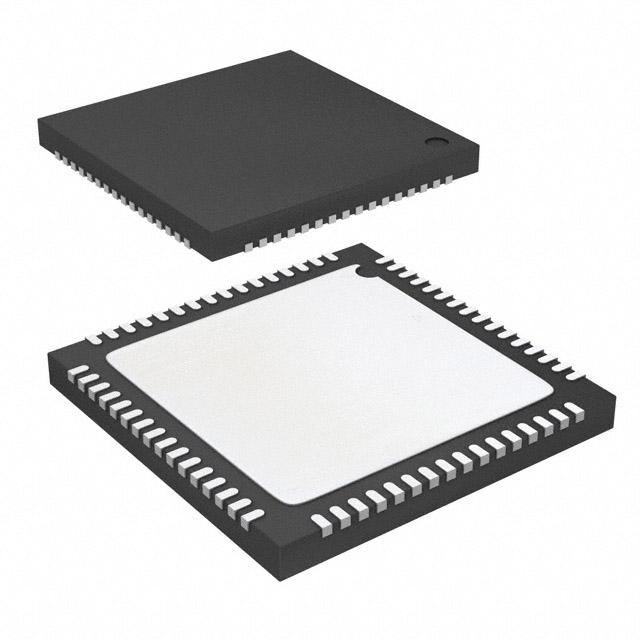
64-lead LQFP Pb-free package
APPLICATIONS
DVD recorders
PC video
HDD-based PVRs/DVDRs
LCD TVs
Set-top boxes
Security systems
Digital televisions
Portable video devices
Automotive entertainment
AVR receiver
GENERAL DESCRIPTION
The ADV7181 integrated video decoder automatically detects
and converts a standard analog baseband television signal
compatible with worldwide standards NTSC, PAL, and SECAM
into 4:2:2 component video data compatible with 16-/8-bit
CCIR601/CCIR656.
The advanced, highly flexible digital output interface enables
performance video decoding and conversion in line-locked
clock-based systems. This makes the device ideally suited for a
broad range of applications with diverse analog video characteristics, including tape-based sources, broadcast sources,
security/surveillance cameras, and professional systems.
The six analog input channels accept standard composite,
S-Video, YPrPb video signals in an extensive number of
combinations. AGC and clamp restore circuitry allow an input
video signal peak-to-peak range of 0.5 V up to 1.6 V.
Alternatively, these can be bypassed for manual settings.
The fixed 54 MHz clocking of the ADCs and datapath for all
modes allow very precise, accurate sampling and digital
filtering. The line-locked clock output allows the output data
rate, timing signals, and output clock signals to be synchronous,
asynchronous, or line locked even with ±5% line length
variation. The output control signals allow glueless interface
connections in almost any application. The ADV7181 modes
are set up over a 2-wire, serial, bidirectional port (I2Ccompatible).
The ADV7181 is fabricated in a 3.3 V CMOS process. Its
monolithic CMOS construction ensures greater functionality
with lower power dissipation.
The ADV7181 is packaged in a small 64-lead LFCSP and LQFP
and Pb-free packages.
Rev. B
Information furnished by Analog Devices is believed to be accurate and reliable.
However, no responsibility is assumed by Analog Devices for its use, nor for any
infringements of patents or other rights of third parties that may result from its use.
Specifications subject to change without notice. No license is granted by implication
or otherwise under any patent or patent rights of Analog Devices. Trademarks and
registered trademarks are the property of their respective owners.
One Technology Way, P.O. Box 9106, Norwood, MA 02062-9106, U.S.A.
Tel: 781.329.4700
www.analog.com
Fax: 781.461.3113
© 2005 Analog Devices, Inc. All rights reserved.
�ADV7181
TABLE OF CONTENTS
Introduction ...................................................................................... 4
Luma Filter.................................................................................. 27
Analog Front End......................................................................... 4
Chroma Filter ............................................................................. 30
Standard Definition Processor ................................................... 4
Gain Operation........................................................................... 31
Functional Block Diagram .............................................................. 5
Chroma Transient Improvement (CTI) .................................. 35
Specifications..................................................................................... 6
Digital Noise Reduction (DNR)............................................... 36
Electrical Characteristics............................................................. 6
Comb Filters ............................................................................... 36
Video Specifications..................................................................... 7
AV Code Insertion and Controls ............................................. 39
Timing Specifications .................................................................. 8
Synchronization Output Signals .............................................. 41
Analog Specifications .................................................................. 8
Sync Processing .......................................................................... 49
Thermal Specifications ................................................................ 8
VBI Data Decode ....................................................................... 50
Timing Diagrams ......................................................................... 9
Pixel Port Configuration ............................................................... 61
Absolute Maximum Ratings.......................................................... 10
MPU Port Description................................................................... 62
ESD Caution................................................................................ 10
Register Accesses........................................................................ 63
Pin Configuration and Function Descriptions........................... 11
Register Programming .............................................................. 63
Analog Front End ........................................................................... 13
I2C Sequencer.............................................................................. 63
Analog Input Muxing ................................................................ 13
Global Control Registers ............................................................... 15
Power-Save Modes ..................................................................... 15
Reset Control .............................................................................. 15
Global Pin Control..................................................................... 16
Global Status Registers................................................................... 18
I2C Control Register Map.......................................................... 64
I2C Register Map Details ........................................................... 67
I2C Programming Examples.......................................................... 93
Mode 1—CVBS Input (Composite Video on AIN6) ............ 93
Mode 2—S-Video Input (Y on AIN1 and C on AIN4)......... 94
Identification............................................................................... 18
Mode 3—525i/625i YPrPb Input (Y on AIN1, Pr on AIN3,
and Pb on AIN5) ........................................................................ 94
Status 1 ......................................................................................... 18
Mode 4—CVBS Tuner Input CVBS PAL on AIN6 ............... 95
Status 2 ......................................................................................... 19
PCB Layout Recommendations.................................................... 96
Status 3 ......................................................................................... 19
Analog Interface Inputs............................................................. 96
Standard Definition Processor (SDP).......................................... 20
Power Supply Decoupling ......................................................... 96
SD Luma Path ............................................................................. 20
PLL ............................................................................................... 96
SD Chroma Path......................................................................... 20
Digital Outputs (Both Data and Clocks) ................................ 96
Sync Processing .......................................................................... 21
Digital Inputs .............................................................................. 97
VBI Data Recovery..................................................................... 21
XTAL and Load Capacitor Value Selection ............................ 97
General Setup.............................................................................. 21
Typical Circuit Connection........................................................... 98
Color Controls ............................................................................ 24
Outline Dimensions ..................................................................... 100
Clamp Operation........................................................................ 26
Ordering Guide ........................................................................ 101
Rev. B | Page 2 of 104
�ADV7181
REVISION HISTORY
3/05—Rev. A to Rev. B
7/04—Rev. 0 to Rev. A
Changes to the Analog Specifications Section ..............................8
Changes to Table 20 and Table 21 ................................................17
Changes to Table 27 and Table 28 ................................................19
Change to Table 50..........................................................................25
Addition to the Clamp Operation Section...................................26
Changes to Figures 11.....................................................................29
Changes to Figures 12, 13, 14 ........................................................30
Changes to Chroma Filter Section ................................................30
Deleted YPM Section and Renumbered Subsequent Tables .....30
Changes to Figure 15 ......................................................................31
Change to the Luma Gain Section ................................................32
Changes to Table 103 and Table 104............................................42
Deleted Table 172 and Renumbered Subsequent Tables............68
Changes to Table 176......................................................................71
Changes to Table 185......................................................................78
Changes to Table 192......................................................................83
Changes to Table 193......................................................................84
Changes to Table 194......................................................................85
Added XTAL and Load Capacitor Value Selection Section ......97
Change to Figure 41 ........................................................................98
Addition to Applications List ..........................................................1
Changes to Table 3 ............................................................................8
Changes to Table 5 ............................................................................8
Replaced Figure 3 ..............................................................................9
Changes to Global Pin Control Section .......................................16
Changes to Table 202 ......................................................................91
Changes to Table 203 ......................................................................92
Added package in Outline Dimensions Section .......................103
Changes to Ordering Guide.........................................................104
5/04—Revision 0: Initial Version
Rev. B | Page 3 of 104
�ADV7181
INTRODUCTION
The ADV7181 is a high quality, single chip, multiformat video
decoder that automatically detects and converts PAL, NTSC,
and SECAM standards in the form of composite, S-Video, and
component video into a digital ITU-R BT.656 format.
The advanced, highly flexible digital output interface enables
performance video decoding and conversion in line-locked
clock-based systems. This makes the device ideally suited for a
broad range of applications with diverse analog video characteristics, including tape-based sources, broadcast sources,
security/surveillance cameras, and professional systems.
ANALOG FRONT END
The ADV7181 analog front end comprises three 9-bit ADCs
that digitize the analog video signal before applying it to the
standard definition processor. The analog front end employs
differential channels to each ADC to ensure high performance
in mixed-signal applications.
The front end also includes a 6-channel input mux that enables
multiple video signals to be applied to the ADV7181. Current
and voltage clamps are positioned in front of each ADC to
ensure that the video signal remains within the range of the
converter. Fine clamping of the video signals is performed
downstream by digital fine clamping within the ADV7181. The
ADCs are configured to run in 4× oversampling mode.
STANDARD DEFINITION PROCESSOR
The ADV7181 is capable of decoding a large selection of
baseband video signals in composite, S-Video, and component
formats. The video standards supported by the ADV7181
include PAL B/D/I/G/H, PAL60, PAL M, PAL N, PAL Nc,
NTSC M/J, NTSC 4.43, and SECAM B/D/G/K/L. The
ADV7181 can automatically detect the video standard and
process it accordingly.
The ADV7181 has a 5-line, superadaptive, 2D comb filter that
gives superior chrominance and luminance separation when
decoding a composite video signal. This highly adaptive filter
automatically adjusts its processing mode according to video
standard and signal quality with no user intervention required.
Video user controls such as brightness, contrast, saturation, and
hue are also available within the ADV7181.
The ADV7181 implements a patented adaptive digital linelength tracking (ADLLT) algorithm to track varying video line
lengths from sources such as a VCR. ADLLT enables the
ADV7181 to track and decode poor quality video sources such
as VCRs, noisy sources from tuner outputs, VCD players, and
camcorders. The ADV7181 contains a chroma transient
improvement (CTI) processor that sharpens the edge rate of
chroma transitions, resulting in sharper vertical transitions.
The ADV7181 can process a variety of VBI data services such as
closed captioning (CC), wide screen signaling (WSS), copy generation management system (CGMS), EDTV, Gemstar 1×/2×,
and extended data service (XDS). The ADV7181 is fully
Macrovision certified; detection circuitry enables Type I, II, and
III protection levels to be identified and reported to the user.
The decoder is also fully robust to all Macrovision signal inputs.
Rev. B | Page 4 of 104
�INPUT
MUX
SCLK
SDA
ALSB
CVBS
S-VIDEO
YPrPb
6
A/D
CLAMP
9
9
9
SERIAL INTERFACE
CONTROL AND VBI DATA
SYNC PROCESSING AND
CLOCK GENERATION
A/D
A/D
CLAMP
CLAMP
Figure 1.
Rev. B | Page 5 of 104
CONTROL
AND DATA
ADV7181
SYNC AND
CLK CONTROL
DECIMATION AND
DOWNSAMPLING
FILTERS
DATA
PREPROCESSOR
9
9
CHROMA
DIGITAL
FINE
CLAMP
STANDARD
AUTODETECTION
MACROVISION
DETECTION
GAIN
CONTROL
LINE
LENGTH
PREDICTOR
GAIN
CONTROL
GLOBAL CONTROL
CHROMA
FILTER
SYNC
EXTRACT
LUMA
FILTER
VBI DATA RECOVERY
CHROMA
DEMOD
FSC
RECOVERY
LUMA
DIGITAL
FINE
CLAMP
STANDARD DEFINITION PROCESSOR
CHROMA
2D COMB
(4H MAX)
CTI
C-DNR
AV
CODE
INSERTION
L-DNR
LUMA
2D COMB
(4H MAX)
FREE RUN
OUTPUT CONTROL
SYNTHESIZED
LLC CONTROL
CHROMA
RESAMPLE
RESAMPLE
CONTROL
LUMA
RESAMPLE
16
8
8
SFL
LLC
FIELD
VS
HS
PIXEL
DATA
04820-001
AIN1–AIN6
ADV7181
FUNCTIONAL BLOCK DIAGRAM
OUTPUT FORMATTER
�ADV7181
SPECIFICATIONS
Temperature range: TMIN to TMAX, –40°C to +85°C. The min/max specifications are guaranteed over this range.
ELECTRICAL CHARACTERISTICS
AVDD = 3.15 V to 3.45 V, DVDD = 1.65 V to 2.0 V, DVDDIO = 3.0 V to 3.6 V, PVDD = 1.65 V to 2.0 V; operating temperature range, unless
otherwise noted.
Table 1.
Parameter
STATIC PERFORMANCE
Resolution (Each ADC)
Integral Nonlinearity
Differential Nonlinearity
DIGITAL INPUTS
Input High Voltage
Input Low Voltage
Input Current
Input Capacitance
DIGITAL OUTPUTS
Output High Voltage
Output Low Voltage
High Impedance Leakage Current
Output Capacitance
POWER REQUIREMENTS1
Digital Core Power Supply
Digital I/O Power Supply
PLL Power Supply
Analog Power Supply
Digital Core Supply Current
Digital I/O Supply Current
PLL Supply Current
Analog Supply Current
Power-Down Current
Power-Up Time
Symbol
Test Conditions
N
INL
DNL
BSL at 54 MHz
BSL at 54 MHz
VIH
VIL
IIN
Min
Typ
Max
Unit
–0.475/+0.6
–0.25/+0.5
9
–1.5/+2
–0.7/+2
Bits
LSB
LSB
0.8
+50
+10
10
V
V
µA
µA
pF
0.4
10
20
V
V
µA
pF
2
Pin 29
All other pins
–50
–10
ISOURCE = 0.4 mA
ISINK = 3.2 mA
2.4
CIN
VOH
VOL
ILEAK
COUT
DVDD
DVDDIO
PVDD
AVDD
IDVDD
IDVDDIO
IPVDD
IAVDD
1.65
3.0
1.65
3.15
CVBS input2
YPrPb input3
IPWRDN
tPWRUP
1
Guaranteed by characterization.
ADC1 and ADC2 powered down.
3
All three ADCs powered on.
2
Rev. B | Page 6 of 104
1.8
3.3
1.8
3.3
80
2
10.5
85
180
1.5
20
2
3.6
2.0
3.45
V
V
V
V
mA
mA
mA
mA
mA
mA
ms
�ADV7181
VIDEO SPECIFICATIONS
Guaranteed by characterization. AVDD = 3.15 V to 3.45 V, DVDD = 1.65 V to 2.0 V, DVDDIO = 3.0 V to 3.6 V, PVDD = 1.65 V to 2.0 V; operating
temperature range, unless otherwise noted.
Table 2.
Parameter
NONLINEAR SPECIFICATIONS
Differential Phase
Differential Gain
Luma Nonlinearity
NOISE SPECIFICATIONS
SNR Unweighted
Analog Front End Crosstalk
LOCK TIME SPECIFICATIONS
Horizontal Lock Range
Vertical Lock Range
Fsc Subcarrier Lock Range
Color Lock In Time
Sync Depth Range
Color Burst Range
Vertical Lock Time
Autodetection Switch Speed
CHROMA SPECIFICATIONS
Hue Accuracy
Color Saturation Accuracy
Color AGC Range
Chroma Amplitude Error
Chroma Phase Error
Chroma Luma Intermodulation
LUMA SPECIFICATIONS
Luma Brightness Accuracy
Luma Contrast Accuracy
Symbol
Test Conditions
DP
DG
LNL
Min
Typ
Max
Unit
CVBS I/P, modulate 5-step
CVBS I/P, modulate 5-step
CVBS I/P, 5-step
0.6
0.6
0.6
0.7
0.7
0.7
°
%
%
Luma ramp
Luma flat field
54
58
60
–5
40
dB
dB
dB
+5
70
±1.3
60
20
5
200
200
2
100
HUE
CL_AC
1
1
0.5
0.5
0.2
°
%
%
%
°
%
1
1
%
%
5
CVBS, 1 V I/P
CVBS, 1 V I/P
Rev. B | Page 7 of 104
%
Hz
kHz
Lines
%
%
Fields
lines
400
�ADV7181
TIMING SPECIFICATIONS
Guaranteed by characterization. AVDD = 3.15 V to 3.45 V, DVDD = 1.65 V to 2.0 V, DVDDIO = 3.0 V to 3.6 V, PVDD = 1.65 V to 2.0 V; operating
temperature range, unless otherwise noted.
Table 3.
Parameter
SYSTEM CLOCK AND CRYSTAL
Nominal Frequency
Frequency Stability
I2C PORT
SCLK Frequency
SCLK Min Pulse Width High
SCLK Min Pulse Width Low
Hold Time (Start Condition)
Setup Time (Start Condition)
SDA Setup Time
SCLK and SDA Rise Time
SCLK and SDA Fall Time
Setup Time for Stop Condition
RESET FEATURE
Reset Pulse Width
CLOCK OUTPUTS
LLC1 Mark Space Ratio
DATA AND CONTROL OUTPUTS
Data Output Transitional Time
Data Output Transitional Time
Symbol
Test Conditions
Min
Typ
Max
Unit
±50
MHz
ppm
27.00
400
t1
t2
t3
t4
t5
t6
t7
t8
0.6
1.3
0.6
0.6
100
300
300
0.6
5
t9:t10
t11
t12
kHz
µs
µs
µs
µs
ns
ns
ns
µs
ms
45:55
55:45
Negative clock edge to start of valid data.
(tACCESS = t10 – t11)
End of valid data to negative clock edge.
(tHOLD = t9 + t12)
% Duty Cycle
6
ns
0.6
ns
ANALOG SPECIFICATIONS
Guaranteed by characterization. At AVDD = 3.15 V to 3.45 V, DVDD = 1.65 V to 2.0 V, DVDDIO = 3.0 V to 3.6 V, PVDD = 1.65 V to 2.0 V;
operating temperature range, unless otherwise noted. Recommended analog input video signal range: 0.5 V – 1.6 V, typically 1 V p-p.
Table 4.
Parameter
CLAMP CIRCUITRY
External Clamp Capacitor
Input Impedance
Large Clamp Source Current
Large Clamp Sink Current
Fine Clamp Source Current
Fine Clamp Sink Current
Symbol
Test Conditions
Min
Clamps switched off
Typ
Max
0.1
10
0.75
0.75
60
60
Unit
µF
MΩ
mA
mA
µA
µA
THERMAL SPECIFICATIONS
Table 5.
Parameter
THERMAL CHARACTERISTICS
Junction-to-Ambient Thermal
Resistance (Still Air)
Junction-to-Case Thermal Resistance
Junction-to-Ambient Thermal
Resistance (Still Air)
Junction-to-Case Thermal Resistance
Symbol
Test Conditions
θJA
4-layer PCB with solid ground plane, 64-lead LFCSP
45.5
°C/W
θJC
θJA
4-layer PCB with solid ground plane, 64-lead LFCSP
4-layer PCB with solid ground plane, 64-lead LQFP
9.2
47
°C/W
°C/W
θJC
4-layer PCB with solid ground plane, 64-lead LQFP
11.1
°C/W
Rev. B | Page 8 of 104
Min
Typ
Max
Unit
�ADV7181
TIMING DIAGRAMS
t3
t5
t3
SDA
t1
t6
t2
t4
t7
04820-002
SCLK
t8
Figure 2. I2C Timing
t9
t10
OUTPUT LLC1
t11
OUTPUTS P0–P15, VS,
HS, FIELD, SFL
Figure 3. Pixel Port and Control Output Timing
Rev. B | Page 9 of 104
04820-003
t12
�ADV7181
ABSOLUTE MAXIMUM RATINGS
Table 6.
Parameter
AVDD to GND
AVDD to AGND
DVDD to DGND
PVDD to AGND
DVDDIO to DGND
DVDDIO to AVDD
PVDD to DVDD
DVDDIO – PVDD
DVDDIO – DVDD
AVDD – PVDD
AVDD – DVDD
Digital Inputs Voltage to DGND
Digital Output Voltage to DGND
Analog Inputs to AGND
Maximum Junction Temperature
(TJ max)
Storage Temperature Range
Infrared Reflow Soldering (20 s)
Rating
4V
4V
2.2 V
2.2 V
4V
–0.3 V to +0.3 V
–0.3 V to +0.3 V
–0.3 V to +2 V
–0.3 V to +2 V
–0.3 V to +2 V
–0.3 V to +2 V
–0.3 V to DVDDIO + 0.3 V
–0.3 V to DVDDIO + 0.3 V
AGND – 0.3 V to AVDD + 0.3 V
150°C
Stresses above those listed under Absolute Maximum Ratings
may cause permanent damage to the device. This is a stress
rating only; functional operation of the device at these or any
other conditions above those indicated in the operational
sections of this specification is not implied. Exposure to
absolute maximum rating conditions for extended periods may
affect device reliability.
–65°C to +150°C
260°C
ESD CAUTION
ESD (electrostatic discharge) sensitive device. Electrostatic charges as high as 4000 V readily accumulate on the
human body and test equipment and can discharge without detection. Although this product features
proprietary ESD protection circuitry, permanent damage may occur on devices subjected to high energy
electrostatic discharges. Therefore, proper ESD precautions are recommended to avoid performance
degradation or loss of functionality.
Rev. B | Page 10 of 104
�ADV7181
VS
FIELD
P12
P13
P14
P15
DVDD
DGND
NC
NC
SCLK
SDATA
ALSB
RESET
NC
AIN6
PIN CONFIGURATION AND FUNCTION DESCRIPTIONS
64
63
62
61
60
59
58
57
56
55
54
53
52
51
50
49
48
AIN5
47
AIN4
DGND 3
46
AIN3
DVDDIO 4
45
AGND
P11 5
44
CAPC2
P10 6
43
AGND
P9 7
42
CML
41
REFOUT
40
AVDD
39
CAPY2
DVDDIO 11
38
CAPY1
NC 12
37
AGND
NC 13
36
AIN2
P7 14
35
AIN1
P6 15
34
DGND
P5 16
33
NC
HS 2
PIN 1
INDICATOR
ADV7181
P8 8
TOP VIEW
(Not to Scale)
SFL 9
26
27
28
29
30
31
32
ELPF
PVDD
AGND
XTAL1
25
PWRDN
LLC
24
NC
P2
23
NC
P3
NC = NO CONNECT
22
P0
21
P1
20
DGND
19
DVDD
18
XTAL
17
P4
DGND 10
04820-004
NC 1
Figure 4. 64-Lead LFCSP/LQFP Pin Configuration
Table 7. Pin Function Descriptions
Pin No.
3, 10, 24, 34, 57
32, 37, 43, 45
4, 11
23, 58
40
31
35, 36, 46–49
1, 12, 13, 27, 28, 33,
50, 55, 56
26, 25, 19, 18, 17,
16, 15, 14, 8, 7, 6, 5,
62, 61, 60, 59
2
64
63
53
54
52
Mnemonic
DGND
AGND
DVDDIO
DVDD
AVDD
PVDD
AIN1–AIN6
NC
Type
G
G
P
P
P
P
I
Function
Digital Ground.
Analog Ground.
Digital I/O Supply Voltage (3.3 V).
Digital Core Supply Voltage (1.8 V).
Analog Supply Voltage (3.3 V).
PLL Supply Voltage (1.8 V).
Analog Video Input Channels.
No Connect Pins.
P0–P15
O
Video Pixel Output Port.
HS
VS
FIELD
SDA
SCLK
ALSB
O
O
O
I/O
I
I
51
RESET
I
20
LLC
O
22
XTAL
I
Horizontal Synchronization Output Signal.
Vertical Synchronization Output Signal.
Field Synchronization Output Signal.
I2C Port Serial Data Input/Output Pin.
I2C Port Serial Clock Input (Max Clock Rate of 400 kHz).
This pin selects the I2C address for the ADV7181. ALSB set to a Logic 0 sets the address for a
write as 0x40; for ALSB set to a logic high, the address selected is 0x42.
System Reset Input, Active Low. A minimum low reset pulse width of 5 ms is required to
reset the ADV7181 circuitry.
This is a line-locked output clock for the pixel data output by the ADV7181. Nominally
27 MHz, but varies up or down according to video line length.
This is the input pin for the 27 MHz crystal, or can be overdriven by an external 3.3 V,
27 MHz clock oscillator source. In crystal mode, the crystal must be a fundamental crystal.
Rev. B | Page 11 of 104
�ADV7181
Pin No.
21
Mnemonic
XTAL1
Type
O
29
PWRDN
I
30
ELPF
I
9
SFL
O
41
REFOUT
O
42
CML
O
38, 39
CAPY1, CAPY2
I
44
CAPC2
I
Function
This pin should be connected to the 27 MHz crystal or left as a no connect if an external
3.3 V, 27 MHz clock oscillator source is used to clock the ADV7181. In crystal mode, the
crystal must be a fundamental crystal.
A logic low on this pin places the ADV7181 in a power-down mode. Refer to the I2C Control
Register Map section for more options on power-down modes for the ADV7181.
The recommended external loop filter must be connected to this ELPF pin, as shown in
Figure 42.
Subcarrier Frequency Lock. This pin contains a serial output stream that can be used to lock
the subcarrier frequency when this decoder is connected to any Analog Devices digital
video encoder.
Internal Voltage Reference Output. Refer to Figure 42 for a recommended capacitor
network for this pin.
Common-Mode Level for the Internal ADCs. Refer to Figure 42 for a recommended
capacitor network for this pin.
ADC’s Capacitor Network. Refer to Figure 42 for a recommended capacitor network for
this pin.
ADC’s Capacitor Network. Refer to Figure 42 for a recommended capacitor network for
this pin.
Rev. B | Page 12 of 104
�ADV7181
ANALOG FRONT END
AIN2
AIN1
AIN4
AIN3
AIN6
AIN5
ADC_SW_MAN_EN
AIN2
AIN1
AIN4
AIN3
AIN6
AIN5
ADC0_SW[3:0]
ADC0
AIN4
AIN3
AIN6
AIN5
ADC1_SW[3:0]
ADC1
AIN6
AIN5
ADC2
04820-005
ADC0_SW[3:0]
Figure 5. Internal Pin Connections
There are two key steps to configure the ADV7181 to correctly
decode the input video. Descriptions of these steps follow.
SETADC_sw_man_en, Manual Input Muxing Enable,
Address C4 [7]
•
The analog input muxing section must be configured to
correctly route the video from the analog input pins to the
correct set of ADCs.
ADC0_sw[3:0], ADC0 mux configuration, Address C3 [3:0]
ADC1_sw[3:0], ADC1 mux configuration, Address C3 [7:4]
ADC2_sw[3:0], ADC2 mux configuration, Address C4 [3:0]
•
The standard definition processor block, which decodes
the digital data, should be configured to process either
CVBS, YC, or YPrPb.
To configure the ADV7181 analog muxing section, the user
must select the analog input (AIN1–AIN6) that is to be
processed by each ADC. SETADC_sw_man_en must be set to 1
to enable the muxing blocks to be configured. The three mux
sections are controlled by the signal buses ADC0/1/2_sw[3:0].
Table 8 explains the control words used.
ANALOG INPUT MUXING
The ADV7181 has an integrated analog muxing section that
allows more than one source of video signal to be connected to
the decoder. Figure 5 outlines the overall structure of the input
muxing provided in the ADV7181.
A maximum of six CVBS inputs can be connected and decoded
by the ADV7181. As seen in the Pin Configuration and
Function Description section, these analog input pins lie in
close proximity to one another. This calls for a careful design of
the PCB layout, for example, ground shielding between all
signals routed through tracks that are physically close together.
It is strongly recommended to connect any unused analog input
pins to AGND to act as a shield.
The input signal that contains the timing information (H/V
syncs) must be processed by ADC0. For example, in YC input
configuration, ADC0 should be connected to the Y channel and
ADC1 to the C channel. In cases where one or more ADCs are
not used to process video, for example, CVBS input, the idle
ADCs should be powered down, (see the ADC Power-Down
Control section).
Restrictions are imposed on the channel routing by the analog
signal routing inside the IC; every input pin cannot be routed to
each ADC. Refer to Table 8 for an overview on the routing
capabilities inside the chip.
Rev. B | Page 13 of 104
�ADV7181
Table 8. Manual Mux Settings for All ADCs
SETADC_sw_man_en = 1
ADC1_sw[3:0]
ADC1 Connected To:
0000
No Connection
0001
No Connection
0010
No Connection
0011
No Connection
0100
AIN4
0101
AIN6
0110
No Connection
0111
No Connection
1000
No Connection
1001
No Connection
1010
No Connection
1011
No Connection
1100
AIN3
1101
AIN5
1110
No Connection
1111
No Connection
ADC0 Connected To:
No Connection
AIN2
No Connection
No Connection
AIN4
AIN6
No Connection
No Connection
No Connection
AIN1
No Connection
No Connection
AIN3
AIN5
No Connection
No Connection
CONNECTING
ANALOG SIGNALS
TO ADV7181
ADC2 Connected To:
No Connection
No Connection
No Connection
No Connection
No Connection
AIN6
No Connection
No Connection
No Connection
No Connection
No Connection
No Connection
No Connection
AIN5
No Connection
No Connection
The INSEL bits allow the user to select the input format. It
configures the Standard Definition Processor core to process
CVBS (Comp), S-Video (Y/C), or Component (YPbPr) format.
SET INSEL[3:0] TO
CONFIGURE ADV7181 TO
DECODE VIDEO FORMAT:
CVBS: 0000
YC: 0110
YPrPb: 1001
CONFIGURE ADC INPUTS USING
MUXING CONTROL BITS
(ADC_sw_man_en,
ADC0_sw,adc1_sw, ADC2_sw)
ADC2_sw[3:0]
0000
0001
0010
0011
0100
0101
0110
0111
1000
1001
1010
1011
1100
1101
1110
1111
INSEL[3:0] Input Selection, Address 0x00 [3:0]
Table 9. Standard Definition Processor Format Selection,
INSEL[3:0]
04820-006
ADC0_sw[3:0]
0000
0001
0010
0011
0100
0101
0110
0111
1000
1001
1010
1011
1100
1101
1110
1111
Figure 6. Input Muxing Overview
INSEL[3:0]
0000
0110
1001
Rev. B | Page 14 of 104
Video Format
Composite
YC
YPrPb
�ADV7181
GLOBAL CONTROL REGISTERS
Register control bits listed in this section affect the whole chip.
POWER-SAVE MODES
PWRDN_ADC_0
0 (default)
1
Power-Down
PDBP, Address 0x0F [2]
There are two ways to shut down the digital core of the
ADV7181: a pin (PWRDN) and a bit (PWRDN see below). The
PDBP controls which of the two has the higher priority. The
default is to give the pin (PWRDN) priority. This allows the
user to have the ADV7181 powered down by default.
Table 10. PDBP Function
PDBP
0 (default)
1
Description
Digital core power controlled by the PWRDN pin
(bit is disregarded).
Bit has priority (pin is disregarded).
PWRDN, Address 0x0F [5]
Setting the PWRDN bit switches the ADV7181 into a chip-wide
power-down mode. The power-down stops the clock from
entering the digital section of the chip, thereby freezing its
operation. No I2C bits are lost during power-down. The
PWRDN bit also affects the analog blocks and switches them
into low current modes. The I2C interface itself is unaffected,
and remains operational in power-down mode.
The ADV7181 leaves the power-down state if the PWRDN bit is
set to 0 (via I2C), or if the overall part is reset using the RESET
pin.
PDBP must be set to 1 for the PWRDN bit to power down the
ADV7181.
Table 11. PWRDN Function
PWRDN
0 (default)
1
PWRDN_ADC_0, Address 0x3A [3]
Table 12. PWRDN_ADC_0 Function
PWRDN_ADC_1, Address 0x3A [2]
Table 13. PWRDN_ADC_1 Function
PWRDN_ADC_1
0 (default)
1
The ADV7181 contains three 9-bit ADCs (ADC 0, ADC 1, and
ADC 2). If required, it is possible to power down each ADC
individually.
PWRDN_ADC_2
0 (default)
1
CVBS mode. ADC 1 and ADC 2 should be powered down
to save on power consumption.
•
S-Video mode. ADC 2 should be powered down to save on
power consumption.
Description
ADC normal operation.
Power down ADC 2.
RESET CONTROL
Chip Reset (RES), Address 0x0F [7]
Setting this bit, equivalent to controlling the RESET pin on the
ADV7181, issues a full chip reset. All I2C registers are reset to
their default values. (Some register bits do not have a reset value
specified. They keep their last written value. Those bits are
marked as having a reset value of x in the register table.) After
the reset sequence, the part immediately starts to acquire the
incoming video signal.
Notes
•
After setting the RES bit (or initiating a reset via the pin),
the part returns to the default mode of operation with
respect to its primary mode of operation. All I2C bits are
loaded with their default values, making this bit selfclearing.
•
Executing a software reset takes approximately 2 ms.
However, it is recommended to wait 5 ms before further
I2C writes are performed.
•
The I2C master controller receives a no acknowledge
condition on the ninth clock cycle when chip reset is
implemented. See the MPU Port Description section.
When should the ADCs be powered down?
•
Description
ADC normal operation.
Power down ADC 1.
PWRDN_ADC_2, Address 0x3A [1]
Table 14. PWRDN_ADC_2 Function
Description
Chip operational.
ADV7181 in chip-wide power-down.
ADC Power-Down Control
Description
ADC normal operation.
Power down ADC 0.
Table 15. RES Function
RES
0 (default)
1
Rev. B | Page 15 of 104
Description
Normal operation.
Start reset sequence.
�ADV7181
Timing Signals Output Enable
GLOBAL PIN CONTROL
Three-State Output Drivers
TIM_OE, Address 0x04 [3]
TOD, Address 0x03 [6]
This bit allows the user to three-state the output drivers of the
ADV7181.
Upon setting the TOD bit, the P15–P0, HS, VS, FIELD, and SFL
pins are three-stated.
The timing pins (HS/VS/FIELD) can be forced active via the
TIM_OE bit. For more information on three-state control, refer
to the following sections:
•
Three-State LLC Driver
•
Timing Signals Output Enable
The TIM_OE bit should be regarded as an addition to the TOD
bit. Setting it high forces the output drivers for HS, VS, and
FIELD into the active (that is, driving) state even if the TOD bit
is set. If set to low, the HS, VS, and FIELD pins are three-stated
depending on the TOD bit. This functionality is useful if the
decoder is to be used as a timing generator only. This may be
the case if only the timing signals are to be extracted from an
incoming signal, or if the part is in free-run mode where a
separate chip can output, for instance, a company logo.
For more information on three-state control, refer to the
following sections:
•
Three-State Output Drivers
Individual drive strength controls are provided via the
DR_STR_XX bits.
•
Three-State LLC Driver
Table 16. TOD Function
Individual drive strength controls are provided via the
DR_STR_XX bits.
TOD
0 (default)
1
Description
Output drivers enabled.
Output drivers three-stated.
Table 18. TIM_OE Function
TIM_OE
0 (default)
1
Three-State LLC Driver
TRI_LLC, Address 0x0E [6]
Description
HS, VS, FIELD three-stated according to the
TOD bit.
HS, VS, FIELD are forced active all the time. The
DR_STR_S[1:0] setting determines drive
strength.
This bit allows the output drivers for the LLC pin of the
ADV7181 to be three-stated. For more information on threestate control, refer to the following sections:
Drive Strength Selection (Data)
•
Three-State Output Drivers
•
Timing Signals Output Enable
For EMC and crosstalk reasons, it may be desirable to
strengthen or weaken the drive strength of the output drivers.
The DR_STR[1:0] bits affect the P[15:0] output drivers.
DR_STR[1:0] Address 0x04 [5:4]
Individual drive strength controls are provided via the
DR_STR_XX bits.
For more information on three-state control, refer to the
following sections:
Table 17. TRI_LLC Function
•
Drive Strength Selection (Clock)
TRI_LLC
0 (default)
•
Drive Strength Selection (Sync)
1
Description
LLC pin drivers working according to the
DR_STR_C[1:0] setting (pin enabled).
LLC pin drivers three-stated.
Table 19. DR_STR Function
DR_STR[1:0]
00
01 (default)
10
11
Rev. B | Page 16 of 104
Description
Low drive strength (1×).
Medium low drive strength (2×).
Medium high drive strength (3×).
High drive strength (4×).
�ADV7181
Drive Strength Selection (Clock)
Enable Subcarrier Frequency Lock Pin
DR_STR_C[1:0] Address 0x0E [3:2]
EN_SFL_PIN Address 0x04 [1]
The DR_STR_C[1:0] bits can be used to select the strength of
the clock signal output driver (LLC pin). For more information,
refer to the following sections:
The EN_SFL_PIN bit enables the output of subcarrier lock
information (also known as GenLock) from the ADV7181 to an
encoder in a decoder-encoder back-to-back arrangement.
•
Drive Strength Selection (Sync)
Table 22. EN_SFL_PIN
•
Drive Strength Selection (Data)
EN_SFL_PIN
0 (default)
1
Table 20. DR_STR_C Function
DR_STR_C[1:0]
00
01 (default)
10
11
Description
Low drive strength (1×).
Medium low drive strength (2×).
Medium high drive strength (3×).
High drive strength (4×).
Polarity LLC Pin
PCLK Address 0x37 [0]
The polarity of the clock that leaves the ADV7181 via the LLC
pin can be inverted using the PCLK bit.
Drive Strength Selection (Sync)
Changing the polarity of the LLC clock output may be
necessary to meet the setup-and-hold time expectations of
follow-on chips.
DR_STR_S[1:0] Address 0x0E [1:0]
The DR_STR_S[1:0] bits allow the user to select the strength of
the synchronization signals with which HS, VS, and F are
driven. For more information, refer to the following sections:
•
Drive Strength Selection (Clock)
•
Drive Strength Selection (Data)
Table 23. PCLK Function
PCLK
0
1 (default)
Table 21. DR_STR_S Function
DR_STR_S[1:0]
00
01 (default)
10
11
Description
Subcarrier frequency lock output is disabled.
Subcarrier frequency lock information is
presented on the SFL pin.
Description
Low drive strength (1×).
Medium low drive strength (2×).
Medium high drive strength (3×).
High drive strength (4×).
Rev. B | Page 17 of 104
Description
Invert LLC output polarity.
LLC output polarity normal (as per the Timing
Diagrams).
�ADV7181
GLOBAL STATUS REGISTERS
Four registers provide summary information about the video
decoder. The IDENT register allows the user to identify the
revision code of the ADV7181. The other three registers contain
status bits from the ADV7181.
Depending on the setting of the FSCLE bit, the Status[0] and
Status[1] are based solely on horizontal timing info or on the
horizontal timing and lock status of the color subcarrier. See the
FSCLE Fsc Lock Enable, Address 0x51 [7] section.
IDENTIFICATION
Autodetection Result
IDENT[7:0] Address 0x11 [7:0]
AD_RESULT[2:0] Address 0x10 [6:4]
Provides identification of the revision of the ADV7181. Review
the list of IDENT code readback values for the various versions
shown in Table 24.
The AD_RESULT[2:0] bits report back on the findings from the
autodetection block. Consult the General Setup sec-tion for
more information on enabling the autodetection block, and the
Autodetection of SD Modes section to find out how to
configure it.
Table 24. IDENT Function
IDENT[7:0]
0x0D
0x0E
0x0F or 0x10
0x11
Description
ADV7181-ES1
ADV7181-ES2
ADV7181-FT
ADV7181 (Version 2)
Table 25. AD_RESULT Function
STATUS 1
STATUS_1[7:0] Address 0x10 [7:0]
This read-only register provides information about the internal
status of the ADV7181.
AD_RESULT[2:0]
000
001
010
011
100
101
110
111
See CIL[2:0] Count Into Lock, Address 0x51 [2:0] and COL[2:0]
Count Out of Lock, Address 0x51 [5:3] for information on the
timing.
Table 26. STATUS 1 Function
STATUS 1 [7:0]
0
1
2
3
4
5
6
7
Bit Name
IN_LOCK
LOST_LOCK
FSC_LOCK
FOLLOW_PW
AD_RESULT.0
AD_RESULT.1
AD_RESULT.2
COL_KILL
Description
In lock (right now).
Lost lock (since last read of this register).
Fsc locked (right now).
AGC follows peak white algorithm.
Result of autodetection.
Result of autodetection.
Result of autodetection.
Color kill active.
Rev. B | Page 18 of 104
Description
NTSM-MJ
NTSC-443
PAL-M
PAL-60
PAL-BGHID
SECAM
PAL-Combination N
SECAM 525
�ADV7181
STATUS 2
STATUS_2[7:0], Address 0x12 [7:0]
Table 27. STATUS 2 Function
STATUS 2 [7:0]
0
1
2
3
4
5
6
7
Bit Name
MVCS DET
MVCS T3
MV_PS DET
MV_AGC DET
LL_NSTD
FSC_NSTD
Reserved
Reserved
Description
Detected Macrovision color striping.
Macrovision color striping protection. Conforms to Type 3 (if high), and Type 2 (if low).
Detected Macrovision pseudo sync pulses.
Detected Macrovision AGC pulses.
Line length is nonstandard.
Fsc frequency is nonstandard.
STATUS 3
STATUS_3[7:0], Address 0x13 [7:0]
Table 28. STATUS 3 Function
STATUS 3 [7:0]
0
1
2
3
4
Bit Name
INST_HLOCK
Reserved
Reserved
Reserved
FREE_RUN_ACT
5
6
7
STD_FLD_LEN
INTERLACED
PAL_SW_LOCK
Description
Horizontal lock indicator (instantaneous).
ADV7181 outputs a blue screen (see the DEF_VAL_AUTO_EN Default Value Automatic
Enable, Address 0x0C [1] section).
Field length is correct for currently selected video standard.
Interlaced video detected (field sequence found).
Reliable sequence of swinging bursts detected.
Rev. B | Page 19 of 104
�ADV7181
STANDARD DEFINITION PROCESSOR (SDP)
STANDARD DEFINITION PROCESSOR
MACROVISION
DETECTION
DIGITIZED CVBS
DIGITIZED Y (YC)
DIGITIZED CVBS
DIGITIZED C (YC)
VBI DATA
RECOVERY
LUMA
DIGITAL
FINE
CLAMP
CHROMA
DIGITAL
FINE
CLAMP
CHROMA
DEMOD
STANDARD
AUTODETECTION
SLLC
CONTROL
LUMA
FILTER
GAIN
CONTROL
LUMA
RESAMPLE
SYNC
EXTRACT
LINE
LENGTH
PREDICTOR
RESAMPLE
CONTROL
CHROMA
FILTER
GAIN
CONTROL
CHROMA
RESAMPLE
LUMA
2D COMB
AV
CODE
INSERTION
CHROMA
2D COMB
VIDEO DATA
OUTPUT
MEASUREMENT
BLOCK (= >12C)
VIDEO DATA
PROCESSING
BLOCK
04820-007
FSC
RECOVERY
Figure 7. Block Diagram of the Standard Definition Processor
A block diagram of the ADV7181’s standard definition
processor is shown in Figure 7.
SD CHROMA PATH
The SDP block can handle standard definition video in CVBS,
YC, and YPrPb formats. It can be divided into a luminance and
chrominance path. If the input video is of a composite type
(CVBS), both processing paths are fed with the CVBS input.
•
Digital Fine Clamp. This block uses a high precision
algorithm to clamp the video signal.
•
Digital Fine Clamp. This block uses a high precision
algorithm to clamp the video signal.
Chroma Demodulation. This block uses a color subcarrier
(Fsc) recovery unit to regenerate the color subcarrier for
any modulated chroma scheme. The demodulation block
then performs an AM demodulation for PAL and NTSC,
and an FM demodulation for SECAM.
•
Luma Filter Block. This block contains a luma decimation
filter (YAA) with a fixed response, and some shaping filters
(YSH) that have selectable responses.
Chroma Filter Block. This block contains a chroma
decimation filter (CAA) with a fixed response, and some
shaping filters (CSH) that have selectable responses.
•
Gain Control. Automatic gain control (AGC) can operate
on several different modes, including gain based on the
color subcarrier’s amplitude, gain based on the depth of the
horizontal sync pulse on the luma channel, or fixed manual
gain.
•
Chroma Resample. The chroma data is digitally resampled
to keep it perfectly aligned with the luma data. The
resampling is done to correct for static and dynamic linelength errors of the incoming video signal.
The input signal is processed by the following blocks:
SD LUMA PATH
The input signal is processed by the following blocks:
•
•
•
Luma Gain Control. The automatic gain control (AGC)
can operate on a variety of different modes, including gainbased on the depth of the horizontal sync pulse, peak white
mode, and fixed manual gain.
•
Luma Resample. To correct for line-length errors as well as
dynamic line-length changes, the data is digitally
resampled.
•
Luma 2D Comb. The two-dimensional comb filter
provides YC separation.
•
•
AV Code Insertion. At this point, the decoded luma (Y)
signal is merged with the retrieved chroma values. AV
codes (as per ITU-R. BT-656) can be inserted.
Chroma 2D Comb. The two-dimensional, 5-line,
superadaptive comb filter provides high quality YC
separation in case the input signal is CVBS.
•
AV Code Insertion. At this point, the demodulated chroma
(Cr and Cb) signal is merged with the retrieved luma
values. AV codes (as per ITU-R. BT-656) can be inserted.
Rev. B | Page 20 of 104
�ADV7181
SYNC PROCESSING
GENERAL SETUP
The ADV7181 extracts syncs embedded in the video data
stream. There is currently no support for external HS/VS
inputs. The sync extraction has been optimized to support
imperfect video sources, for example, videocassette recorders
with head switches. The actual algorithm used employs a coarse
detection based on a threshold crossing followed by a more
detailed detection using an adaptive interpolation algorithm.
The raw sync information is sent to a line-length measurement
and prediction block. The output is then used to drive the
digital resampling section to ensure that the ADV7181 outputs
720 active pixels per line.
Video Standard Selection
The sync processing on the ADV7181 includes two specialized
postprocessing blocks that filter and condition the raw sync
information retrieved from the digitized analog video.
•
VSYNC processor. This block provides extra filtering of the
detected VSYNCs to give improved vertical lock.
•
HSYNC processor. The HSYNC processor is designed to
filter incoming HSYNCs that have been corrupted by
noise, providing much improved performance for video
signals with stable time base but poor SNR.
The VID_SEL[3:0] register allows the user to force the digital
core into a specific video standard. Under normal circumstances,
this should not be necessary. The VID_SEL[3:0] bits default to
an autodetection mode that supports PAL, NTSC, SECAM, and
variants thereof.
Refer to the Autodetection of SD Modes section for more
information on the autodetection system.
Autodetection of SD Modes
In order to guide the autodetect system of the ADV7181,
individual enable bits are provided for each of the supported
video standards. Setting the relevant bit to 0 inhibits the
standard from being detected automatically. Instead, the system
picks the closest of the remaining enabled standards. The results
of the autodetection can be read back via the status registers.
See the Global Status Registers section for more information.
Table 29. VID_SEL Function
VID_SEL[3:0]
Address 0x00 [7:4]
0000 (default)
VBI DATA RECOVERY
The ADV7181 can retrieve the following information from the
input video:
•
Wide-screen signaling (WSS)
•
Copy generation management system (CGMS)
•
Closed caption (CC)
•
Macrovision protection presence
•
EDTV data
•
Gemstar-compatible data slicing
0001
0010
0011
The ADV7181 is capable of automatically detecting the
incoming video standard with respect to color subcarrier
frequency, field rate, and line rate.
It can configure itself to support PAL-BGHID, PAL-M/N,
PAL-combination N, NTSC-M, NTSC-J, SECAM 50 Hz/60 Hz,
NTSC4.43, and PAL60.
0100
0101
0110
0111
1000
1001
1010
1011
1100
1101
1110
1111
Rev. B | Page 21 of 104
Description
Autodetect (PAL BGHID) NTSC J
(no pedestal), SECAM.
Autodetect (PAL BGHID) NTSC M
(pedestal), SECAM.
Autodetect (PAL N) NTSC J (no
pedestal), SECAM.
Autodetect (PAL N) NTSC M
(pedestal), SECAM.
NTSC J (1)
NTSC M (1).
PAL60.
NTSC4.43 (1).
PAL BGHID.
PAL N (= PAL BGHID (with pedestal)).
PAL M (without pedestal).
PAL M.
PAL combination N.
PAL combination N (with pedestal).
SECAM.
SECAM (with pedestal).
�ADV7181
AD_SEC525_EN Enable Autodetection of SECAM 525
Line Video, Address 0x07 [7]
Table 30. AD_SEC525_EN Function
AD_NTSC_EN Enable Autodetection of NTSC,
Address 0x07 [1]
Table 36. AD_NTSC_EN Function
AD_SEC525_EN
0 (default)
AD_NTSC_EN
0
1 (default)
1
Description
Disable the autodetection of a 525-line
system with a SECAM style, FM-modulated
color component.
Enable the detection.
AD_PAL_EN Enable Autodetection of PAL,
Address 0x07 [0]
Table 37. AD_PAL_EN Function
AD_SECAM_EN Enable Autodetection of SECAM,
Address 0x07 [6]
Table 31. AD_SECAM_EN Function
AD_SECAM_EN
0
1 (default)
AD_PAL_EN
0
1 (default)
Description
Disable the autodetection of SECAM.
Enable the detection.
1 (default)
This bit controls the behavior of the PAL switch bit in the SFL
(GenLock Telegram) data stream. It was implemented to solve
some compatibility issues with video encoders. It solves two
problems:
Description
Disable the autodetection of NTSC style
systems with a 4.43 MHz color subcarrier.
Enable the detection.
•
The PAL switch bit is only meaningful in PAL. Some
encoders (including Analog Devices encoders) also look
at the state of this bit in NTSC.
•
There was a design change in Analog Devices encoders
from ADV717x to ADV719x. The older versions used the
SFL (GenLock Telegram) bit directly, while the later ones
invert the bit prior to using it. This is because the inversion
compensated for the 1-line delay of an SFL (GenLock
Telegram) transmission.
AD_P60_EN Enable Autodetection of PAL60,
Address 0x07 [4]
Table 33. AD_P60_EN Function
AD_P60_EN
0
1 (default)
Description
Disable the detection of standard PAL.
Enable the detection.
SFL_INV Subcarrier Frequency Lock Inversion
AD_N443_EN Enable Autodetection of NTSC443,
Address 0x07 [5]
Table 32. AD_N443_EN Function
AD_N443_EN
0
Description
Disable the detection of standard NTSC.
Enable the detection.
Description
Disable the autodetection of PAL systems
with a 60 Hz field rate.
Enable the detection.
As a result:
•
AD_PALN_EN Enable Autodetection of PAL N,
Address 0x07 [3]
Table 34. AD_PALN_EN Function
ADV717x encoders need the PAL switch bit in the SFL
(GenLock Telegram) to be 1 for NTSC to work.
•
ADV7190/ADV7191/ADV7194 encoders need the PAL
switch bit in the SFL to be 0 to work in NTSC.
AD_PALN_EN
0
1 (default)
If the state of the PAL switch bit is wrong, a 180°phase shift
occurs.
Description
Disable the detection of the PAL N standard.
Enable the detection.
AD_PALM_EN Enable Autodetection of PAL M,
Address 0x07 [2]
Table 35. AD_PALM_EN Function
AD_PALM_EN
0
1 (default)
Description
Disable the autodetection of PAL M.
Enable the detection.
In a decoder/encoder back-to-back system in which SFL is used,
this bit must be set up properly for the specific encoder used.
Table 38. SFL_INV Function
SFL_INV
Address 0x41 [6]
0
1 (default)
Rev. B | Page 22 of 104
Description
SFL-compatible with ADV7190/ADV7191/
ADV7194 encoders.
SFL-compatible with ADV717x/ADV7173x
encoders.
�ADV7181
Lock Related Controls
CIL[2:0] Count Into Lock, Address 0x51 [2:0]
Lock information is presented to the user through Bits [1:0] of
the Status 1 register. See the STATUS_1[7:0] Address 0x10 [7:0]
section. Figure 8 outlines the signal flow and the controls
available to influence the way the lock status information is
generated.
CIL[2:0] determine the number of consecutive lines for which
the into lock condition must be true before the system switches
into the locked state, and reports this via Status 0 [1:0].
SRLS Select Raw Lock Signal, Address 0x51 [6]
Using the SRLS bit, the user can choose between two sources for
determining the lock status (per Bits [1:0] in the Status 1 register).
•
The time_win signal is based on a line-to-line evaluation of
the horizontal synchronization pulse of the incoming
video. It reacts quite quickly.
•
The free_run signal evaluates the properties of the
incoming video over several fields, and takes vertical
synchronization information into account.
CIL[2:0]
000
001
010
011
100 (default)
101
110
111
Description (Count Value in Lines of Video)
1
2
5
10
100
500
1000
100000
COL[2:0] Count Out of Lock, Address 0x51 [5:3]
COL[2:0] determine the number of consecutive lines for which
the out of lock condition must be true before the system switches
into the unlocked state, and reports this via Status 0 [1:0].
Table 39. SRLS Function
SRLS
0 (default)
1
Table 41. CIL Function
Description
Select the free_run signal.
Select the time_win signal.
Table 42. COL Function
FSCLE Fsc Lock Enable, Address 0x51 [7]
The FSCLE bit allows the user to choose whether or not the
status of the color subcarrier loop is taken into account when
the overall lock status is determined and presented via Bits [1:0]
in Status Register 1. This bit must be set to 0 when operating the
ADV7181 in YPrPb component mode in order to generate a
reliable HLOCK status bit.
COL[2:0]
000
001
010
011
100 (default)
101
110
111
Description (Count Value in Lines of Video)
1
2
5
10
100
500
1000
100000
Table 40. FSCLE Function
1 (default)
Description
Overall lock status only dependent on
horizontal sync lock.
Overall lock status dependent on horizontal
sync lock and Fsc Lock.
SELECT THE RAW LOCK SIGNAL
SRLS
TIME_WIN
1
FREE_RUN
0
FILTER THE RAW LOCK SIGNAL
CIL[2:0], COL[2:0]
0
1
FSC LOCK
COUNTER INTO LOCK
COUNTER OUT OF LOCK
STATUS 1 [0]
MEMORY
STATUS 1 [1]
04820-008
FSCLE
0
TAKE FSC LOCK INTO ACCOUNT
FSCLE
Figure 8. Lock Related Signal Path
Rev. B | Page 23 of 104
�ADV7181
COLOR CONTROLS
The following registers provide user control over the picture
appearance, including control of the active data in the event of
video being lost. They are independent of any other controls.
For instance, brightness control is independent from picture
clamping, although both controls affect the signal’s dc level.
SD_SAT_Cr[7:0] SD Saturation Cr Channel,
Address 0xE4 [7:0]
This register allows the user to control the gain of the Cr
channel only.
Table 43. CON Function
For this register to be active, SAT[7:0] must be programmed
with its default value of 0x80. If SAT[7:0] is programmed with a
different value, SD_SAT_Cb[7:0] and SD_SAT_Cr[7:0] are
inactive.
CON[7:0]
Table 46. SD_SAT_Cr Function
CON[7:0] Contrast Adjust, Address 0x08 [7:0]
This register allows the user to adjust the contrast of the picture.
0x80 (default)
0x00
0xFF
Description
(Adjust Contrast of the Picture)
Gain on luma channel = 1.
Gain on luma channel = 0.
Gain on luma channel = 2.
SD_SAT_Cr[7:0]
0x80 (default)
0x00
0xFF
Description
(Adjust Saturation of the Picture)
Gain on Cr channel = 0 dB.
Gain on Cr channel = –42 dB.
Gain on Cr channel = +6 dB.
SAT[7:0] Saturation Adjust, Address 0x09 [7:0]
The user can adjust the saturation of the color output using this
register.
ADI encourages users not to use the SAT[7:0] register, which
may be removed in future revisions of the ADV7181. Instead,
the SD_SAT_Cb and SD_SAT_Cr registers should be used.
SD_OFF_Cb[7:0] SD Offset Cb Channel, Address 0xE1 [7:0]
This register allows the user to select an offset for the Cb
channel only. There is a functional overlap with the Hue [7:0]
register.
Table 47.SD_OFF_Cb Function
Table 44. SAT Function
SAT[7:0]
0x80 (default)
0x00
0xFF
Description
(Adjust Saturation of the Picture)
Chroma gain = 0 dB.
Chroma gain = –42 dB.
Chroma gain = 6 dB.
SD_OFF_Cb[7:0]
0x80 (default)
0x00
0xFF
Description
(Adjust Hue of the Picture by Selecting
an Offset for Data on the Cb Channel)
0 offset applied to the Cb channel.
–312 mV offset applied to the Cb channel.
+312 mV offset applied to the Cb channel.
SD_OFF_Cr [7:0] SD Offset Cr Channel, Address 0xE2 [7:0]
SD_SAT_Cb[7:0] SD Saturation Cb Channel,
Address 0xE3 [7:0]
This register allows the user to select an offset for the Cr
channel only. There is a functional overlap with the Hue [7:0]
register.
This register allows the user to control the gain of the Cb
channel only.
Table 48. SD_OFF_Cr Function
For this register to be active, SAT[7:0] must be programmed
with its default value of 0x80. If SAT[7:0] is programmed with a
different value, SD_SAT_Cb[7:0] and SD_SAT_Cr[7:0] are
inactive.
Table 45. SD_SAT_Cb Function
SD_SAT_Cb[7:0]
0x80 (defualt)
0x00
0xFF
SD_OFF_Cr[7:0]
0x80 (default)
0x00
0xFF
Description
(Adjust Saturation of the Picture)
Gain on Cb channel = 0 dB.
Gain on Cb channel = –42 dB.
Gain on Cb channel = +6 dB.
Rev. B | Page 24 of 104
Description
(Adjust Hue of the Picture by Selecting
an Offset for Data on Cr Channel)
0 offset applied to the Cb channel.
–312 mV offset applied to the Cr channel.
+312 mV offset applied to the Cr channel.
�ADV7181
BRI[7:0] Brightness Adjust, Address 0x0A [7:0]
Table 51. DEF_Y Function
This register controls the brightness of the video signal through
the ADV7181.
DEF_Y[5:0]
0x0D (blue) (default)
Description
Default value of Y.
Table 49. BRI Function
BRI[7:0]
0x00 (default)
0x7F
0x80
Description
(Adjust Brightness of the Picture)
Offset of the luma channel = 0IRE.
Offset of the luma channel = 100IRE.
Offset of the luma channel = –100IRE.
DEF_C[7:0] Default Value C, Address 0x0D [7:0]
The DEF_C[7:0] register complements the DEF_Y[5:0] value.
It defines the 4 MSBs of Cr and Cb values to be output if
HUE[7:0] Hue Adjust, Address 0x0B [7:0]
This register contains the value for the color hue adjustment.
HUE[7:0] has a range of ±90°, with 0x00 equivalent to an
adjustment of 0°. The resolution of HUE[7:0] is 1 bit = 0.7°.
The hue adjustment value is fed into the AM color demodulation
block. Therefore, it only applies to video signals that contain
chroma information in the form of an AM modulated carrier
(CVBS or Y/C in PAL or NTSC). It does not affect SECAM and
does not work on component video inputs (YPrPb).
Table 50. HUE Function
HUE[7:0]
0x00 (default)
0x7F
0x80
Description (Adjust Hue of the Picture)
Phase of the chroma signal = 0°.
Phase of the chroma signal = +90°.
Phase of the chroma signal = –90°.
•
The DEF_VAL_AUTO_EN bit is set to high and the
ADV7181 can’t lock to the input video (automatic mode).
•
DEF_VAL_EN bit is set to high (forced output).
The data that is finally output from the ADV7181 for the
chroma side is Cr[7:0] = {DEF_C[7:4], 0, 0, 0, 0}, Cb[7:0] =
{DEF_C[3:0], 0, 0, 0, 0}.
Table 52. DEF_C Function
DEF_C[7:0]
0x7C (blue) (default)
DEF_VAL_EN Default Value Enable, Address 0x0C [0]
This bit forces the use of the default values for Y, Cr, and Cb.
Refer to the descriptions for DEF_Y and DEF_C for additional
information. The decoder also outputs a stable 27 MHz clock,
HS, and VS in this mode.
Table 53. DEF_VAL_EN Function
DEF_VAL_EN
0 (default)
DEF_Y[5:0] Default Value Y, Address 0x0C [7:2]
When the ADV7181 loses lock on the incoming video signal or
when there is no input signal, the DEF_Y[5:0] register allows
the user to specify a default luma value to be output.
Description
Default values for Cr and Cb.
1
This value is used under the following conditions:
Description
Don't force the use of default Y, Cr, and
Cb values. Output colors dependent on
DEF_VAL_AUTO_EN.
Always use default Y, Cr, and Cb values.
Override picture data even if the video
decoder is locked.
•
If DEF_VAL_AUTO_EN bit is set to high and the
ADV7181 lost lock to the input video signal. This is the
intended mode of operation (automatic mode).
DEF_VAL_AUTO_EN Default Value Automatic Enable,
Address 0x0C [1]
•
The DEF_VAL_EN bit is set, regardless of the lock status of
the video decoder. This is a forced mode that may be useful
during configuration.
Table 54. DEF_VAL_AUTO_EN Function
The DEF_Y[5:0] values define the 6 MSBs of the output video.
The remaining LSBs are padded with 0s. For example, in 8-bit
mode, the output is Y[7:0] = {DEF_Y[5:0], 0, 0}.
This bit enables the automatic usage of the default values for Y,
Cr, and Cb when the ADV7181 cannot lock to the video signal.
DEF_VAL_AUTO_EN
0
1 (default)
Rev. B | Page 25 of 104
Description
Don't use default Y, Cr, and Cb values. If
unlocked, output noise.
Use default Y, Cr, and Cb values when
the decoder loses lock.
�ADV7181
CLAMP OPERATION
COARSE
CURRENT
SOURCES
ANALOG
VIDEO
INPUT
ADC
DATA
PRE
PROCESSOR
(DPP)
SDP
WITH DIGITAL
FINE CLAMP
04820-009
FINE
CURRENT
SOURCES
CLAMP CONTROL
Figure 9. Clamping Overview
The input video is ac-coupled into the ADV7181 through a
0.1 µF capacitor. It is recommended that the range of the input
video signal is 0.5 V to 1.6 V (typically 1 V p-p). If the signal
exceeds this range, it cannot be processed correctly in the
decoder. Since the input signal is ac-coupled into the decoder,
its dc value needs to be restored. This process is referred to as
clamping the video. This section explains the general process of
clamping on the ADV7181 and shows the different ways in
which a user can configure its behavior.
The ADV7181 uses a combination of current sources and a
digital processing block for clamping, as shown in Figure 9.
The analog processing channel shown is replicated three times
inside the IC. While only one single channel (and only one
ADC) would be needed for a CVBS signal, two independent
channels are needed for YC (S-VHS) type signals, and three
independent channels are needed to allow component signals
(YPrPb) to be processed.
The clamping can be divided into two sections:
The clamping scheme has to complete two tasks: it must be able
to acquire a newly connected video signal with a completely
unknown dc level, and it must maintain the dc level during
normal operation.
For a fast acquiring of an unknown video signal, the large
current clamps may be activated. (It is assumed that the
amplitude of the video signal at this point is of a nominal
value.) Control of the coarse and fine current clamp parameters
is performed automatically by the decoder.
Standard definition video signals may have excessive noise on
them. In particular, CVBS signals transmitted by terrestrial
broadcast and demodulated using a tuner usually show very
large levels of noise (>100 mV). A voltage clamp would be
unsuitable for this type of video signal. Instead, the ADV7181
employs a set of four current sources that can cause coarse
(>0.5 mA) and fine (