±150°/Sec Yaw Rate Gyroscope
ADXRS623
FEATURES
GENERAL DESCRIPTION
Complete rate gyroscope on a single chip
Z-axis (yaw rate) response
High vibration rejection over wide frequency
2000 g powered shock survivability
Ratiometric to referenced supply
5 V single-supply operation
–40°C to +105°C operation
Self-test on digital command
Ultrasmall and light ( 1000 for all typical performance plots, unless otherwise noted.
30
PERCENT OF POPULATION (%)
20
15
10
5
25
20
15
10
2.4
2.5
2.6
2.7
2.8
2.9
3.0
RATEOUT (V)
0
−10
−6
−4
−2
0
2
4
6
8
10
PERCENT DRIFT (%)
Figure 4. Null Output at 25°C (VRATIO = 5 V)
Figure 7. Sensitivity Drift over Temperature
45
45
40
40
PERCENT OF POPULATION (%)
35
30
25
20
15
10
35
30
25
20
15
10
5
5
(°/s/°C)
0
–1200
0.5
–1100
0.4
–1000
0.3
–900
0.2
–800
0.1
–700
0
–500
–0.4 –0.3 –0.2 –0.1
08890-005
0
–0.5
–600
PERCENT OF POPULATION (%)
−8
08890-008
2.3
–1400
2.2
1400
2.1
08890-009
2.0
–1300
0
08890-007
5
08890-004
PERCENT OF POPULATION (%)
25
ST1 Δ (mV)
Figure 5. Null Drift over Temperature (VRATIO = 5 V)
Figure 8. ST1 Output Change at 25°C (VRATIO = 5 V)
45
35
40
PERCENT OF POPULATION (%)
25
20
15
10
5
35
30
25
20
15
10
5
1300
1200
1100
1000
900
800
700
500
14.00
08890-006
13.75
13.50
13.25
13.00
12.75
12.50
12.25
12.00
11.75
11.25
11.50
SENSITIVITY (mV/°/s)
600
0
0
11.00
PERCENT OF POPULATION (%)
30
ST2 Δ (mV)
Figure 9. ST2 Output Change at 25°C (VRATIO = 5 V)
Figure 6. Sensitivity at 25°C (VRATIO = 5 V)
Rev. A | Page 6 of 12
�ADXRS623
30
40
PERCENT OF POPULATION (%)
20
15
10
5
30
25
20
15
10
5
125
135
145
155
165
175
185
0
08890-010
0
195
MEASUREMENT RANGE (°/s)
2.40 2.42 2.44 2.46 2.48 2.50 2.52 2.54 2.56 2.58 2.60
VOLTAGE (V)
Figure 10. Measurement Range
08890-013
PERCENT OF POPULATION (%)
35
25
Figure 13. VTEMP Output at 25°C (VRATIO = 5 V)
3.3
1.5
3.1
1.0
2.9
ST2
2.7
VOLTAGE (V)
VOLTAGE (V)
0.5
0
−0.5
2.5
2.3
2.1
ST1
1.9
−1.0
1.7
0
20
40
60
80
100
120
TEMPERATURE (°C)
08890-011
−20
1.5
–40
0
20
40
60
80
100
120
TEMPERATURE (°C)
Figure 14. VTEMP Output over Temperature (VRATIO = 5 V)
Figure 11. Typical Self-Test Change over Temperature
30
60
REF
Y
X
+45°
–45°
50
25
40
20
(g OR °/s)
30
15
20
10
10
0
5
0
2.5
2.7
2.9
3.1
3.3
3.5
3.7
3.9
4.1
4.3
CURRENT CONSUMPTION (mA)
4.5
–20
750
770
790
810
830
TIME (ms)
Figure 12. Current Consumption at 25°C (VRATIO = 5 V)
Figure 15. g and g × g Sensitivity for a 50 g, 10 ms Pulse
Rev. A | Page 7 of 12
850
08890-015
–10
08890-012
PERCENT OF POPULATION (%)
–20
08890-014
256 PARTS
−1.5
−40
�ADXRS623
0.10
2.0
LATITUDE
LONGITUDE
RATE
1.8
1.6
1.2
(°/s)
PEAK RATEOUT (°/s)
0.05
1.4
1.0
0
0.8
0.6
–0.05
0.4
1k
FREQUENCY (Hz)
10k
–0.10
08890-016
0
100
0
20
40
60
80
100
120
140
TIME (Hours)
08890-019
0.2
Figure 19. Typical Shift in 90 Sec Null Averages Accumulated
over 140 Hours
Figure 16. Typical Response to 10 g Sinusoidal Vibration
(Sensor Bandwidth = 2 kHz)
0.10
400
300
DUT1 OFFSET BY +200°/s
0.05
200
(°/s)
(°/s)
100
0
0
–100
DUT2 OFFSET BY –200°/s
–200
–0.05
0
50
100
150
200
250
(ms)
–0.10
08890-017
–400
0
600
1200
1800
2400
3000
3600
TIME (Seconds)
08890-020
–300
Figure 20. Typical Shift in Short-Term Null (Bandwidth = 1 Hz)
Figure 17. Typical High g (2500 g) Shock Response
(Sensor Bandwidth = 40 Hz)
0.1
0.1
0.01
(°/s rms)
(°/s/ Hz rms)
1
0.1
1
10
100
1k
10k
100k
AVERAGE TIME (Seconds)
0.0001
10
08890-018
0.001
0.01
100
1k
10k
100k
FREQUENCY (Hz)
Figure 21. Typical Noise Spectral Density (Bandwidth = 40 Hz)
Figure 18. Typical Root Allan Deviation at 25°C vs. Averaging Time
Rev. A | Page 8 of 12
08890-021
0.001
0.01
�ADXRS623
THEORY OF OPERATION
SETTING BANDWIDTH
External Capacitor COUT is used in combination with the
on-chip ROUT resistor to create a low-pass filter to limit the
bandwidth of the ADXRS623 rate response. The –3 dB
frequency set by ROUT and COUT is
f OUT =
1
(2 × π × ROUT × COUT )
and can be well controlled because ROUT is trimmed during
manufacturing to be 180 kΩ ± 1%. Any external resistor applied
between the RATEOUT pin (1B, 2A) and the SUMJ pin (1C,
2C) results in
ROUT =
0.1
0.01
0.001
0.0001
0.000001
10
100
1k
10k
100k
FREQUENCY (Hz)
08890-022
0.00001
Figure 22. Noise Spectral Density with Additional 250 Hz Filter
TEMPERATURE OUTPUT AND CALIBRATION
It is common practice to temperature-calibrate gyroscopes to
improve their overall accuracy. The ADXRS623 has a temperature proportional voltage output that provides input to such a
calibration method. The temperature sensor structure is shown
in Figure 23. The temperature output is characteristically
nonlinear, and any load resistance connected to the TEMP
output results in decreasing the TEMP output and temperature
coefficient. Therefore, buffering the output is recommended.
The voltage at the TEMP pin (3F, 3G) is nominally 2.5 V at
25°C and VRATIO = 5 V. The temperature coefficient is ~9 mV/°C
at 25°C. Although the TEMP output is highly repeatable, it has
only modest absolute accuracy.
VTEMP
VRATIO
(180 kΩ × REXT )
(180 kΩ + REXT )
RFIXED
RTEMP
08890-023
The electrostatic resonator requires 18 V to 20 V for operation.
Because only 5 V are typically available in most applications, a
charge pump is included on chip. If an external 18 V to 20 V
supply is available, the two capacitors on CP1 through CP4 can
be omitted, and this supply can be connected to the CP5 pin
(6D, 7D). Note that CP5 should not be grounded when power is
applied to the ADXRS623. Although no damage occurs, under
certain conditions, the charge pump may fail to start up after
the ground is removed without first removing power from the
ADXRS623.
Figure 22 shows the effect of adding a 250 Hz filter to the
output of an ADXRS623 set to 40 Hz bandwidth (as shown
in Figure 21). High frequency demodulation artifacts are
attenuated by approximately 18 dB.
(°/s/ Hz rms)
The ADXRS623 operates on the principle of a resonator
gyroscope. Two polysilicon sensing structures each contain a
dither frame that is electrostatically driven to resonance,
producing the necessary velocity element to produce a Coriolis
force while rotating. At two of the outer extremes of each frame,
orthogonal to the dither motion, are movable fingers that are
placed between fixed pickoff fingers to form a capacitive pickoff
structure that senses Coriolis motion. The resulting signal is fed
to a series of gain and demodulation stages that produce the
electrical rate signal output. The dual-sensor design rejects
external g forces and vibration. Fabricating the sensor with
signal conditioning electronics preserves signal integrity in
noisy environments.
Figure 23. ADXRS623 Temperature Sensor Structure
In general, an additional hardware or software filter is added to
attenuate high frequency noise arising from demodulation
spikes at the gyroscope’s 14 kHz resonant frequency (the noise
spikes at 14 kHz can be clearly seen in the power spectral
density curve shown in Figure 21). Typically, the corner
frequency of this additional filter is set to greater than 5× the
required bandwidth to preserve good phase response.
CALIBRATED PERFORMANCE
Using a three-point calibration technique, it is possible to
calibrate the null and sensitivity drift of the ADXRS623 to an
overall accuracy of nearly 200°/hour. An overall accuracy of
40°/hour or better is possible using more points.
Limiting the bandwidth of the device reduces the flat-band
noise during the calibration process, improving the measurement accuracy at each calibration point.
Rev. A | Page 9 of 12
�ADXRS623
ADXRS623 AND SUPPLY RATIOMETRICITY
SELF-TEST FUNCTION
The ADXRS623 RATEOUT and TEMP signals are ratiometric
to the VRATIO voltage; that is, the null voltage, rate sensitivity, and
temperature outputs are proportional to VRATIO. Thus, the
ADXRS623 is most easily used with a supply-ratiometric ADC
that results in self-cancellation of errors due to minor supply
variations. There is some small error due to nonratiometric
behavior. Typical ratiometricity error for null, sensitivity, selftest, and temperature output is outlined in Table 4.
The ADXRS623 includes a self-test feature that actuates each of
the sensing structures and associated electronics as if subjected
to angular rate. It is activated by standard logic high levels
applied to Input ST1 (5F, 5G), Input ST2 (4F, 4G), or both. ST1
causes the voltage at RATEOUT to change about −1.0 V, and
ST2 causes an opposite change of +1.0 V. The self-test response
follows the viscosity temperature dependence of the package
atmosphere, approximately 0.25%/°C.
Note that VRATIO must never be greater than AVCC.
Activating both ST1 and ST2 simultaneously is not damaging.
ST1 and ST2 are fairly closely matched (±5%), but actuating
both simultaneously may result in a small apparent null bias
shift proportional to the degree of self-test mismatch.
Table 4. Ratiometricity Error for Various Parameters
Parameter
ST1
Mean
Sigma
ST2
Mean
Sigma
Null
Mean
Sigma
Sensitivity
Mean
Sigma
VTEMP
Mean
Sigma
VS = VRATIO = 4.85 V
VS = VRATIO = 5.15 V
0.3%
0.21%
0.09%
0.19%
−0.15%
0.22%
−0.2%
0.2%
−0.3%
0.2%
−0.05%
0.08%
0.003%
0.06%
−0.25%
0.06%
−0.2%
0.05%
−0.04%
0.06%
ST1 and ST2 are activated by applying a voltage of greater than
0.8 × VRATIO to the ST1 and ST2 pins. ST1 and ST2 are deactivated by applying a voltage of less than 0.2 × VRATIO to the ST1
and ST2 pins. The voltage applied to ST1 and ST2 must never
be greater than AVCC.
CONTINUOUS SELF-TEST
NULL ADJUSTMENT
The nominal 2.5 V null is for a symmetrical swing range at
RATEOUT (1B, 2A). However, a nonsymmetrical output swing
may be suitable in some applications. Null adjustment is
possible by injecting a suitable current to SUMJ (1C, 2C). Note
that supply disturbances may reflect some null instability.
Digital supply noise should be avoided, particularly in this case.
The one-chip integration of the ADXRS623 gives it higher
reliability than is obtainable with any other high volume
manufacturing method. In addition, it is manufactured under
a mature BiMOS process with field-proven reliability. As an
additional failure detection measure, a power-on self-test can be
performed. However, some applications may warrant continuous
self-test while sensing rate. Details about continuous self-test
techniques are available in the AN-768 Application Note, Using
the ADXRS150/ADXRS300 in Continuous Self-Test Mode, available at www.analog.com.
Rev. A | Page 10 of 12
�ADXRS623
OUTLINE DIMENSIONS
A1 BALL
CORNER
7.05
6.85 SQ
6.70
*A1 CORNER
INDEX AREA
7
6
5
4
3
2
1
A
B
4.80
BSC SQ
0.80
BSC
C
D
E
F
G
TOP VIEW
BOTTOM VIEW
DETAIL A
3.80 MAX
0.60
0.55
0.50
SEATING
PLANE
3.20 MAX
2.50 MIN
COPLANARITY
0.15
BALL DIAMETER
*BALL A1 IDENTIFIER IS GOLD PLATED AND CONNECTED
TO THE D/A PAD INTERNALLY VIA HOLES.
10-26-2009-B
DETAIL A
0.60 MAX
0.25 MIN
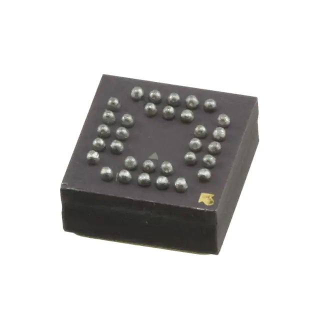
Figure 24. 32-Lead Ceramic Ball Grid Array [CBGA]
(BG-32-3)
Dimensions shown in millimeters
ORDERING GUIDE
Model1, 2
ADXRS623BBGZ
ADXRS623BBGZ-RL
ADXRS623WBBGZ
ADXRS623WBBGZ-RL
EVAL-ADXRS623Z
1
2
Temperature Range
–40°C to +105°C
–40°C to +105°C
–40°C to +105°C
–40°C to +105°C
Package Description
32-Lead Ceramic Ball Grid Array (CBGA)
32-Lead Ceramic Ball Grid Array (CBGA)
32-Lead Ceramic Ball Grid Array (CBGA)
32-Lead Ceramic Ball Grid Array (CBGA)
Evaluation Board
Package Option
BG-32-3
BG-32-3
BG-32-3
BG-32-3
Z = RoHS Compliant Part.
W = Qualified for Automotive Applications.
AUTOMOTIVE PRODUCTS
The ADXRS623W models are available with controlled manufacturing to support the quality and reliability requirements of automotive
applications. Note that these automotive models may have specifications that differ from the commercial models; therefore, designers
should review the Specifications section of this data sheet carefully. Only the automotive grade products shown are available for use in
automotive applications. Contact your local Analog Devices account representative for specific product ordering information and to
obtain the specific Automotive Reliability reports for these models.
Rev. A | Page 11 of 12
�ADXRS623
NOTES
©2010 Analog Devices, Inc. All rights reserved. Trademarks and
registered trademarks are the property of their respective owners.
D08890-0-11/10(A)
Rev. A | Page 12 of 12
�


 工商网监
湘ICP备2023018690号
工商网监
湘ICP备2023018690号
