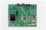
ADSP-CM419F EZ-KIT ® Manual
Revision 1.0, April 2016
Part Number
82-000723-01
Analog Devices, Inc.
One Technology Way
Norwood, MA 02062-9106
�Copyright Information
© 2016 Analog Devices, Inc., ALL RIGHTS RESERVED. This document may not be reproduced in any form
without prior, express written consent from Analog Devices, Inc.
Printed in the USA.
Disclaimer
Analog Devices, Inc. reserves the right to change this product without prior notice. Information furnished by Analog Devices is believed to be accurate and reliable. However, no responsibility is assumed by Analog Devices for its
use; nor for any infringement of patents or other rights of third parties which may result from its use. No license is
granted by implication or otherwise under the patent rights of Analog Devices, Inc.
Trademark and Service Mark Notice
The Analog Devices logo, Blackfin, Blackfin+, SHARC, SHARC+, CrossCore, VisualDSP++, EZ-KIT, EZ-Extender, and EngineerZone are registered trademarks of Analog Devices, Inc.
All other brand and product names are trademarks or service marks of their respective owners.
Regulatory Compliance
The ADSP-CM419F EZ-KIT ® is designed to be used solely in a laboratory environment. The board is not intended for use as a consumer-end product or as a portion of a consumer-end product. The board is an open system
design, which does not include a shielded enclosure and, therefore, may cause interference to other electrical devices
in close proximity. This board should not be used in or near any medical equipment or RF devices.
The ADSP-CM419F EZ-KIT ® is in the process of being certified to comply with the essential requirements of the
European EMC directive 2004/108/EC and, therefore, carries the “CE” mark.
ADSP-CM419F EZ-KIT ® Manual
i
�The ADSP-CM419F EZ-KIT ® contains ESD (electrostatic discharge) sensitive devices. Electrostatic charges readily
accumulate on the human body and equipment and can discharge without detection. Permanent damage may occur
on devices subjected to high-energy discharges. Proper ESD precautions are recommended to avoid performance degradation or loss of functionality. Store unused boards in the protective shiping package.
ADSP-CM419F EZ-KIT ® Manual
ii
�Contents
Preface
Purpose of This Manual................................................................................................................................. 1–1
Intended Audience......................................................................................................................................... 1–1
Manual Contents ........................................................................................................................................... 1–2
Technical Support .......................................................................................................................................... 1–2
Supported Processors ..................................................................................................................................... 1–3
Supported Tools............................................................................................................................................. 1–3
Product Information ...................................................................................................................................... 1–3
Analog Devices Website.............................................................................................................................. 1–3
EngineerZone ............................................................................................................................................. 1–4
Notation Conventions ................................................................................................................................... 1–4
Using the Board
Product Overview .......................................................................................................................................... 2–1
Package Contents........................................................................................................................................... 2–3
Default Configuration ................................................................................................................................... 2–3
IAR Embedded WorkBench Setup ................................................................................................................. 2–4
Debug Interface ............................................................................................................................................. 2–6
Power-On-Self Test........................................................................................................................................ 2–6
Analog Input Channel Selection .................................................................................................................... 2–6
Power Architecture......................................................................................................................................... 2–7
Power Measurements ..................................................................................................................................... 2–7
Example Programs ......................................................................................................................................... 2–7
Reference Design Information ....................................................................................................................... 2–7
ADSP-CM419F EZ-KIT ® Manual
iii
�32M-bit Serial Flash Memory with Dual and Quad SPI (W25Q32).............................................................. 2–8
USB to UART (FT232R)............................................................................................................................... 2–8
Signal and Power Isolated CAN Transceiver (ADM3053).............................................................................. 2–9
Isolated Single Channel RS-232 Line Driver/Receiver (ADM3251E) .......................................................... 2–10
Isolated, Dual Channel RS-232 Line Driver/Receiver (ADM3252E) ........................................................... 2–10
Unity-Gain Stable, Ultralow Distortion, 1 nV/√Hz Voltage Noise, High Speed Op Amp (ADA4899) ........ 2–11
Ultralow Noise, LDO XFET Voltage References with Current Sink and Source (ADR441B) ...................... 2–11
36 V Precision, 2.8 nV/√Hz Rail-to-Rail Output Op Amp (AD8675) ......................................................... 2–12
Ultraprecision, 36 V, 2.8 nV/√Hz Dual Rail-to-Rail Output Op Amp (AD8676)........................................ 2–12
1 ppm 20-Bit, ±1 LSB INL, Voltage Output DAC (AD5791) ..................................................................... 2–13
Isolated, 5 kV, DC-to-DC Converter (ADUM6000).................................................................................... 2–13
Isolated Sigma-Delta Modulator (AD7401) ................................................................................................. 2–13
4K I2C Serial EEPROM (24AA04).............................................................................................................. 2–14
2.2 TFT LCD .............................................................................................................................................. 2–14
Hardware Reference
System Architecture ....................................................................................................................................... 3–1
Switches......................................................................................................................................................... 3–2
Reset Pushbutton ( SW6 )............................................................................................................................ 3–2
GPIO Pushbuttons ( SW1-5 )..................................................................................................................... 3–3
Pushbutton Enable ( SW7 ) ......................................................................................................................... 3–3
SPI Flash Enable ( SW8 )............................................................................................................................. 3–3
LED Enable ( SW9 ) .................................................................................................................................... 3–4
Jumpers ......................................................................................................................................................... 3–4
Boot Mode Select ( JP1 )............................................................................................................................ 3–5
VDD_INT Regulator Select ( JP2 ) ........................................................................................................... 3–6
CAN Interface ( JP4 and JP5 ) ............................................................................................................... 3–6
iv
ADSP-CM419F EZ-KIT ® Manual
�UART Interface( JP6 and JP7 ) .............................................................................................................. 3–6
VREF Source ( JP8 - JP10 ) ................................................................................................................... 3–7
ADC VIN0 A0 ( JP11 - JP14 ) .............................................................................................................. 3–7
AIN DUT ( JP15 - JP37 )...................................................................................................................... 3–8
DC Bias Source( JP38 and JP39 ) .......................................................................................................... 3–8
SINC Interface( JP40 ) .............................................................................................................................. 3–8
Main Power Select ( JP44 ) ........................................................................................................................ 3–8
DC Bias Select ( P5 ) .................................................................................................................................. 3–9
Isolated Power ( P15 ) ................................................................................................................................ 3–9
Single Ended Input ( P16 ) ......................................................................................................................... 3–9
AD7401 Power ( P17 ) ............................................................................................................................... 3–9
Current Measurement ( P20 and P21 ).................................................................................................... 3–9
LEDs ........................................................................................................................................................... 3–10
Power ( LED1 ) ......................................................................................................................................... 3–10
GPIO ( LED2-3 ) ..................................................................................................................................... 3–11
Reset ( LED4 )........................................................................................................................................... 3–11
Fault ( LED5 ) ........................................................................................................................................... 3–11
Connectors .................................................................................................................................................. 3–11
Clock ( J1 and J2 ) .................................................................................................................................. 3–12
Analog Interface ( J3 ).............................................................................................................................. 3–13
PWM Interface ( J4 )............................................................................................................................... 3–13
DAC0 VOUT( J5 ) .................................................................................................................................. 3–13
CAN ( J6 and J7 ) ................................................................................................................................ 3–13
UART ( J8 and J9 ) .............................................................................................................................. 3–14
ADC Input ( J10-J13, J15 and J16 ) ............................................................................................... 3–14
DC Bias ( J17 )........................................................................................................................................ 3–14
Sense ( J18 )............................................................................................................................................. 3–14
LCD ( J19 and J20 ) ............................................................................................................................ 3–15
Character Display ( J21 ) ......................................................................................................................... 3–15
ADSP-CM419F EZ-KIT ® Manual
v
�Debug ( P1 and P2 )................................................................................................................................. 3–15
USB ( P3 ) ................................................................................................................................................ 3–15
AFE Supply ( P6 - P9, P11 and P12 )............................................................................................... 3–15
Power ( P19 )............................................................................................................................................ 3–16
vi
ADSP-CM419F EZ-KIT ® Manual
�Preface
1 Preface
Thank you for purchasing the Analog Devices, Inc. ADSP-CM419F EZ-KIT ® evaluation system.
The ADSP-CM419F processor is based on the ARM® Cortex®-M4 prprocessor core with floatingpoint unit operating at frequencies up to 240 MHz, and the ARM® Cortex-M0TM processor core operating at frequencies up to
100 MHz. The processors integrate up to 160K Bytes of SRAM memory with ECC, up to 1M Byte of flash memory with ECC, accelerators and peripherals optimized for motor control and photo-voltaic (PV) inverter control, and
an analog front end consisting of up to two 6 times simultaneous sampling 16-bit SAR-type ADCs, one 14-bit SAR
monitor ADC and one 12-bit DAC. The EZ-KIT ships with all of the necessary hardware to get you up and running and start the evaluation immediately.
The EZ-KIT contains an analog interface and PWM/digital interface. These interfaces are provided for connecting
with daughter boards to expand on the functionality of the EZ-KIT.
The evaluation board is designed to be used in conjunction with the IAR Embedded Workbench®and Segger®
development environment for advanced application code development and debug such as:
• Create, compile, assemble, and link application programs written in C++, C, and assembly
• Load, run, step, halt, and set breakpoints in application programs
• Read and write data and program memory
• Read and write core and peripheral registers
Purpose of This Manual
This manual provides instructions for installing the product hardware (board). The text describes operation and
configuration of the board components and provides guidelines for running code on the board.
Intended Audience
The primary audience for this manual is a programmer who is familiar with an ARM Cortex-M4 core. The ADSPCM41x family of mixed-signal control processors is based on the ARM Cortex-M4 core.
ADSP-CM419F EZ-KIT ® Manual
1–1
�Manual Contents
For additional information about the Analog Devices processor, see the Hardware Reference Manual. The document
describes the core and memory architecture of the ADSP-CM41x processor, but does not provide detailed
programming information for the ARM core.
The applicable documentation for programming the ARM Cortex-M4 core includes:
• Cortex-M4 Devices Generic User Guide
• CoreSight ETM-M4 Technical Reference Manual
• Cortex-M4 Technical Reference Manual
For more information about programming the ARM core, visit the ARM Information Center:
http://infocenter.arm.com/help/.
Manual Contents
The manual consists of:
• Using the board
Provides basic board information.
• Hardware Reference
Provides information about the hardware aspects of the board.
• Bill of Matrials
A companion file in PDF format that lists all of the components used on the board is available in the installation directory for the Board Support Package (BSP) and on http://www.analog.com/ADSPCM419FEZKIT .
• Schematic
A companion file in PDF format documenting all of the circuits used on the board is available in the installation directory for the Board Support Package (BSP) and on http://www.analog.com/ADSPCM419FEZKIT .
Technical Support
You can reach Analog Devices processors and DSP technical support in the following way
• Post your questions in the processors and DSP support community at EngineerZone®:
http://ez.analog.com/community/dsp
• Submit your questions to technical support directly at:
http://www.analog.com/support
• E-mail your questions about processors, DSPs, and tools development software from CrossCore Embedded Studio or VisualDSP++®:
1–2
ADSP-CM419F EZ-KIT ® Manual
�Supported Processors
If using CrossCore Embeded Studio or VisualDSP++ choose Help > Email Support. This creates an e-mail to
processor.tools.support@analog.com and automatically attaches your CrossCore Embedded Studio or VisualDSP++ version information and license.dat file.
• E-mail your questions about processors and processor applications to:
processor.tools.support@analog.com
processor.china@analog.com
• Contact your Analog Devices sales office or authorized distributor. Locate one at:
http://www.analog.com/adi-sales
• Send questions by mail to:
Analog Devices, Inc.
One Technology Way
P.O. Box 9106
Norwood, MA 02062-9106
USA
Supported Processors
This evaluation system supports the Analog Devices ADSP-CM419Fprocessor.
Supported Tools
Information about code development tools for the ADSP-CM419F EZ-KIT ® and ADSP-CM41x family of processors is available at:
http://www.analog.com/ADSPCM419FEZKIT
Product Information
Product information can be obtained from the Analog Devices Website
Analog Devices Website
The Analog Devices website, http://www.analog.com, provides information about a broad range of products - analog integrated circuits, amplifiers, converters, and digital signal processors.
To access a complete technical library for each processor family, go to http://www.analog.com/processors/technical_library. The manuals selection opens a list of current manuals related to the product as well as a link to the
previous revisions of the manuals. When locating your manual title, note a possible errata check mark next to the
title that leads to the current correction report against the manual.
ADSP-CM419F EZ-KIT ® Manual
1–3
�Product Information
Also note, MyAnalog.com is a free feature of the Analog Devices website that allows customization of a web page to
display only the latest information about products you are interested in. You can choose to receive weekly e-mail
notifications containing updates to the web pages that meet your interests, including documentation errata against
all manuals. MyAnalog.com provides access to books, application notes, data sheets, code examples, and more.
Visit MyAnalog.com to sign up. If you are a registered user, just log on. Your user name is your e-mail address.
EngineerZone
EngineerZone is a technical support forum from Analog Devices, Inc. It allows you direct access to ADI technical
support engineers. You can search FAQs and technical information to get quick answers to your embedded processing and DSP design questions.
Use EngineerZone to connect with other DSP developers who face similar design challenges. You can also use this
open forum to share knowledge and collaborate with the ADI support team and your peers. Visit http://
ez.analog.com to sign up.
Notation Conventions
Text conventions used in this manual are identified and described as follows. Additional conventions, which apply
only to specific chapters, may appear throughout this document.
Example
Description
File > Close
Titles in bold style indicate the location of an item within the CrossCore Embedded Studio IDE’s menu system (for example, the Close command appears on the
File menu).
{this | that}
Alternative required items in syntax descriptions appear within curly brackets and
separated by vertical bars; read the example as this or that. One or the other is
required.
[this | that]
Optional items in syntax descriptions appear within brackets and separated by
vertical bars; read the example as an optional this or that.
[this, …]
Optional item lists in syntax descriptions appear within brackets delimited by
commas and terminated with an ellipsis; read the example as an optional commaseparated list of this.
.SECTION
Commands, directives, keywords, and feature names are in text with letter
gothic font.
filename
Non-keyword placeholders appear in text with letter gothic font and italic
style format.
NOTE:
NOTE: For correct operation, ..
A note provides supplementary information on a related topic. In the online version of this book, the word NOTE: appears instead of this symbol.
1–4
ADSP-CM419F EZ-KIT ® Manual
�Notation Conventions
Example
Description
CAUTION:
CAUTION: Incorrect device operation may result if ..
CAUTION: Device damage may result if ..
A caution identifies conditions or inappropriate usage of the product that could
lead to undesirable results or product damage. In the online version of this book,
the word CAUTION: appears instead of this symbol.
ATTENTION:
ATTENTION: Injury to device users may result if ..
A warning identifies conditions or inappropriate usage of the product that could
lead to conditions that are potentially hazardous for devices users. In the online
version of this book, the word ATTENTION: appears instead of this symbol.
ADSP-CM419F EZ-KIT ® Manual
1–5
�Using the Board
2 Using the Board
This chapter provides information on the major components and peripherals on the board along with instrustions
for installing and setting up the emualtion software.
Product Overview
The board features:
• Analog Devices ADSP-CM419F processor
• 210 ball BGA
• 16 and 30 MHz oscillators
• Analog Interface
• Analog Devices Unity-Gain Stable, Ultralow Distortion, 1 nV/√Hz Voltage Noise, High Speed Op Amp
(ADA4899)
• Analog Devices Ultralow Noise, LDO XFET Voltage References with Current Sink and Source
(ADR441B)
• Analog Devices 1 ppm 20-Bit, ±1 LSB INL, Voltage Output DAC (AD5791)
• LCD
• 2.2 inch TFT LCD module
• SPI Flash (SPI0) chip
• Microchip 4K I2C Serial EEPROM (24AA04)
• Universal Asynchronous Receiver/Transmitter (UART0)
• Analog Devices Isolated Single Channel RS-232 Line Driver/Receiver (ADM3251E)
• DB9
• Universal Asynchronous Receiver/Transmitter (UART3)
• FTDI USB to UART (FT232R)
ADSP-CM419F EZ-KIT ® Manual
2–1
�Product Overview
• USB mini-B
• Universal Asynchronous Receiver/Transmitter (UART4)
• Analog Devices Isolated, Dual Channel RS-232 Line Driver/Receiver (ADM3252E)
• DB9
• CAN
• Analog Devices Signal and Power Isolated CAN Transceiver (ADM3053)
• RJ11
• SINC
• Analog Devices Isolated, 5 kV, DC-to-DC Converter (ADUM6000)
• Analog Devices Isolated Sigma-Delta Modulator (AD7401)
• Debug (JTAG/SWD/SWO) interface
• J-Link Lite emulator
• JTAG/SWD/SWO 20-pin 0.1” header
• JTAG/SWD/SWO 20-pin 0.05” header
• LEDs
• Five LEDs: one power (green), one board reset (red), two general-purpose (amber) and one fault (red)
• Pushbuttons
• Six pushbuttons: one reset and five IRQ/Flag
• Analog connector
• ADC
• AGND/GND/VREF/5V
• PWM connector
• PWM0-2
• SINC0
• SPI1
• SPORT0
• TWI0
• TMR0
• GPIOs
2–2
ADSP-CM419F EZ-KIT ® Manual
�Package Contents
• CNT0-3
• RESET
• GND/3.3V/5V output
• External power supply
• CE compliant
• 5V @3.6 Amps
• Power measurement
• 0.051-ohm resistors for measuring current draw
Package Contents
Your ADSP-CM419F EZ-KIT ® package contains the following items.
• ADSP-CM419F EZ-KIT ® board
• Universal 5V DC power supply
• USB 2.0 type A to mini-B cable
• J-Link Lite emulator
Contact the vendor where you purchased your EZ-KIT or contact Analog Devices, Inc. if any item is missing.
Default Configuration
The ADSP-CM419F EZ-KIT ® board is designed to run as a standalone unit.
The Default Hardware Setup figure shows the default settings for jumpers and switches and the location of the
jumpers, switches, connectors, and LEDs. Confirm that your board is in the default configuration before using the
board.
ADSP-CM419F EZ-KIT ® Manual
2–3
�IAR Embedded WorkBench Setup
J9
J8
J18
P19
J7
J6
SW6
P16
JP7
LED4
P3
P15
JP40
JP6
JP44
P17
JP42
JP43
JP41
P20
JP4
JP5
P21
JP10
P2
J17
JP9
P1
LED5
JP8
J2
JP29
JP28
JP15
JP16
JP32
JP31
JP33
JP21
JP30
JP20
JP18
JP14
JP26
JP11
JP12
JP13
JP27
SW8
J1
J21
J19
JP2
J20
JP38
JP39
JP1
JP23
JP19
JP22
JP24
JP34
JP25
JP35
JP36
P8
JP17
P5
P7
P6
J10
J12
J15
P11
JP37
SW9
SW2
P12
SW5
SW1
J14
SW3
J5
J11
J13
J16
SW7
SW4
LED1
LED3
J4
J3
LED2
Figure 2-1: Default Hardware Setup
IAR Embedded WorkBench Setup
For information about the IAR Embedded Workbench®and Segger® product and software download, go to:
http://www.iar.com/en/Products/IAR-Embedded-Workbench.
The ADSP-CM419F EZ-KIT ® software, based on the IAR Embedded WorkBench, can be found at:
http://www.analog.com/ADSPCM419FEZKIT
Follow these instructions to ensure correct operation of the product software and hardware.
2–4
ADSP-CM419F EZ-KIT ® Manual
�IAR Embedded WorkBench Setup
1. Connect the EZ-KIT board to a personal computer (PC) running IAR Embedded WorkBench, using a JLink/J-Trace emulator:
a. Plug one side of the USB cable into the USB connector of the emulator. Plug the other side into a USB
port of the PC running IAR Embedded WorkBench.
b. Attach the emulator to the header connector, P1 or P2 , on the EZ-KIT board.
2. Attach the provided cord and appropriate plug to the 5V power adapter:
a. Plug the jack-end of the power adapter into the power connector P19 on the EZ-KIT board.
b. Plug the other side of the power adapter into a power outlet. The power LED ( LED1 ) is lit green when
power is applied to the board.
It is assumed that the IAR Embedded WorkBench software is installed and running on your PC.
1. Navigate to the IAR Embedded WorkBench environment via the Start menu.
2. Choose File > Open > Workspace to open a workspace for the project to download and debug.
3. Choose Project > Options.
The General Options, Target page appears.
4. In Processor variant, ensure Device is Analog Devices CM41x
5. Choose Debugger in the Category pane.
The Debugger, Setup options page appears.
a. In Driver, choose J-Link/J-Trace as the emulator to be used to debug the target board.
b. Click the Download tab. The Debugger, Download options page appears.
c. Ensure Use flash loader(s) is enabled. Note that other download settings are optional.
6. Choose Debugger > J-Link/J-Trace in the Category pane.
The emulator Setup options page appears.
a. On the Setup page,
• In Reset, select Connect during reset from the drop-down list.
• In JTAG/SWD speed, select Auto.
• (Optional) In Clock setup, change the default values.
b. On the Connection page,
• In Communication, select USB and Device 0.
• In Interface, select SWD.
7. Click OK to save the emulator settings.
ADSP-CM419F EZ-KIT ® Manual
2–5
�Debug Interface
8. Choose Project > Debug and Download to download the project and start debugging.
Debug Interface
The EZ-KIT provides a JTAG/SWD/SWO connection via .
Power-On-Self Test
The Power-On-Self-Test Program (POST) tests all EZ-KIT peripherals and validates functionality as well as connectivity to the processor. Once assembled, each EZ-KIT is fully tested for an extended period of time with POST. All
EZ-KITs boards are shipped with POST preloaded into flash memory. The POST is executed by resetting the board
and pressing the proper push button(s). The POST also can be used as a reference for a custom software design or
hardware troubleshooting.
Note that the source code for the POST program is included in the Board Support Package (BSP) along with the
readme.txt file that describes how the board is configured to run POST.
Analog Input Channel Selection
The ADSP-CM419F EZ-KIT ® has 24 Primary ADC Input Channels & 7 Secondary ADC Input Channels as follows:
• Primary
• A0 - A7
• B0 - B7
• C0 - C7
• Secondary
• D0 - D7
Multiple input options are available for the ADC Inputs. These include:
• Expansion Interface
• On-board precision DAC
• Op-amp based conditionint of signals via SMC connector
There are 6 SMC connectors on board (J10, J11, J12, J13, J15, J16) that connects to the signal conditioning circuits (DUTs). Each Input can select between two such DUTs.
The inputs can also select between expansion interface or the DAC output. Note that DAC output is not available
on all channels. By default, all inputs (except A0) are connected to the expansion interface via resistors that need to
be installed. The input channel A0 is provided with jumpers on all four selections.
2–6
ADSP-CM419F EZ-KIT ® Manual
�Power Architecture
Power Architecture
Digital Supply
The ADSP-CM419F EZ-KIT ® has two primary voltage domains: 3.3V and 1.2V. The main input is a 5V wall
adaptor. The 5V source can be selected via JP44 to input from the PWM connector (J4) as an alternative to the
wall power adaptor. Refer to J4 and JP44 for details. The Analog Devices ADM7172 LDO provides 3.3V for the
VDD_EXT signal and the 3.3V power requirements of the board. The VDD_INT signal is delivered through either
Analog Devices regulator ADP1715 Linear Regulator (VR2) or a PNP transistor (Q1). Jumper JP2 is provided to
select between External and Internal regulator.
Analog Front End
The Analog Front End is powered via VDD_ANA0 and VDD_ANA1 power pins which fall in 3.3V domain. The
Fast Over Current Protection (FOCP) Comparators are powered via VDD_COMP. By default, analog supplies are
powered from the ADM7172 LDO which powers up the VDD_EXT and rest of the 3.3V domain. External supplies can power up the analog domain via P6, P7 & P8. A +/-5V supply (via P11) is required for the Op Amps at
the input of the Analog Input Channels. A +/-15V supply is required for the DAC AD5791.
Power Measurements
Locations are provided for measuring the current draw from various power planes. Precision 0.051 ohm shunt resistors are available on the 3.3V and VDD_EXT voltage domains. For current draw, the jumper is removed, voltage
across the resistor can be measured using an oscilloscope, and the value of the resistor can be measured using a precision multi-meter. Once voltage and resistance are measured, the current can be calculated by dividing the voltage by
the resistance. For the highest accuracy, a differential probe should be used for measuring the voltage across the resistor.
Example Programs
Example programs are provided with the ADSP-CM419F EZ-KIT ® Board Support Package (BSP) to demonstrate
various capabilities of the product. The programs can be found in the ADSP-CM419F_EZ-KIT\examples installation folder. Refer to a readme file provided with each example for more information.
Reference Design Information
A reference design info package is available for download on the Analog Devices Web site. The package provides
information on the schematic design, layout, fabrication, and assembly of the board.
The information can be found at:
http://www.analog.com/ADSPCM419FEZKIT .
ADSP-CM419F EZ-KIT ® Manual
2–7
�32M-bit Serial Flash Memory with Dual and Quad SPI (W25Q32)
32M-bit Serial Flash Memory with Dual and Quad SPI
(W25Q32)
The W25Q32BV (32 Mb) Serial Flash memory provides a storage solution for systems with limited space, pins and
power. The 25Q series offers flexibility and performance well beyond ordinary Serial Flash devices. They are ideal
for code shadowing to RAM, executing code directly from Dual/Quad SPI (XIP) and storing voice, text and data.
The device operates on a single 2.7V to 3.6V power supply with current consumption as low as 4 mA active and 1
uA for power-down.
The W25Q32BV array is organized into 16,384 programmable pages of 256 bytes each. Up to 256 bytes can be
programmed at a time. Pages can be erased in a group of 16 (4 KB sector erase), groups of 128 (32 KB block erase),
groups of 256 (64 KB block erase) or the entire chip (chip erase). The W25Q32BV has 1024 erasable sectors and 64
erase blocks respectively. The small 4 KB sectors allow for greater flexibility in applications that require data and
parameter storage.
The W25Q32BV supports the standard Serial Peripheral Interface (SPI), and a high performance Dual/Quad ouput
as well as Dual/Quad I/O SPI: Serial Clock, Chip Select, Serial Data I/O0 (DI), I/O1 (DO), I/O2 (WP), and I/O3
(/HOLD). SPI clock frequencies of up to 104 MHz are supported, providing equivalent clock rates of 208 MHz
(104 MHz x 2) for Dual I/O and 320 MHz (80 MHz x 4) for Quad I/O when using Fast Read Dual/Quad I/O
instructions. These transfer rates can outperform standard Asynchronous 8 and 16-bit Parallel Flash memories. The
Continous Read Mode allows for efficient memory access with as few as 8-clocks of instruction-overhead to read a
24-bit address, allowing true XIP (execute in place) operation.
USB to UART (FT232R)
The FT232R is a USB-to-serial-UART interface with the following advanced features:
• Single chip USB to asynchronous serial data transfer interface
• Entire USB protocol handled on the chip. No USB specific firmware programming required
• Fully-integrated 1024 bit EEPROM storing device descriptors and CBUS I/O configuration
• Fully-integrated USB termination resistors
• Fully-integrated clock generation with no external crystal required, plus optional clock output selection enabling a glue-less interface to external MCU or FPGA
• Data transfer rates from 300 baud to 3 Mbaud (RS422, RS485, RS232) at TTL levels
• 128 byte receive buffer and 256 byte transmit buffer utilising buffer smoothing technology to allow for highdata throughput
• FTDI’s royalty-free Virtual Com Port (VCP) and Direct (D2XX) drivers eliminate the requirement for USB
driver development in most cases.
• Transmit and receive LED drive signals
2–8
ADSP-CM419F EZ-KIT ® Manual
�Signal and Power Isolated CAN Transceiver (ADM3053)
• UART interface support for 7 or 8 data bits, 1 or 2 stop bits and odd / even / mark / space / no parity
• FIFO receives and transmits buffers for high-data throughput
• Device supplied pre-programmed with unique USB serial number
• Supports bus powered, self-powered and high-power bus powered USB configurations
• Integrated +3.3V level converter for USB I/O
• Integrated level converter on UART and CBUS for interfacing to between +1.8V and +5V logic
• True 5V/3.3V/2.8V/1.8V CMOS drive output and TTL input
• Configurable I/O pin output drive strength
• Integrated power-on-reset circuit
• Fully-integrated AVCC supply filtering - no external filtering required.
• UART signal inversion option
• +3.3V (using external oscillator) to +5.25V (internal oscillator) single supply operation
• Low-operating and USB suspend current
• Low USB bandwidth consumption
• UHCI/OHCI/EHCI host controller compatible
• USB 2.0 full speed compatible
Signal and Power Isolated CAN Transceiver (ADM3053)
The ADM3053 is an isolated controller area network (CAN) physical layer transceiver with an integrated isolated
dc-to-dc converter. The ADM3053 complies with the ISO 11898 standard.
The device employs Analog Devices, Inc., iCoupler® technology to combine a 2-channel isolator, a CAN transceiver, and Analog Devices isoPower® dc-to-dc converter into a single SOIC surface mount package. An on-chip oscillator outputs a pair of square waveforms that drive an internal transformer to provide isolated power. The device is
powered by a single 5 V supply realizing a fully isolated CAN solution.
The ADM3053 creates a fully isolated interface between the CAN protocol controller and the physical layer bus. It
is capable of running at data rates of up to 1 Mbps.
The device has current limiting and thermal shutdown features to protect against output short circuits. The part is
fully specified over the industrial temperature range and is available in a 20-lead, wide-body SOIC package.
The ADM3053 contains isoPower technology that uses high frequency switching elements to transfer power
through the transformer. Special care must be taken during printed circuit board (PCB) layout to meet emissions
standards. Refer to the AN-0971 Application Note, Control of Radiated Emissions with isoPower Devices, for details on board layout considerations.
ADSP-CM419F EZ-KIT ® Manual
2–9
�Isolated Single Channel RS-232 Line Driver/Receiver (ADM3251E)
Isolated Single Channel RS-232 Line Driver/Receiver
(ADM3251E)
The ADM3251E1 is a high speed, 2.5 kV fully isolated, single-channel RS-232/V.28 transceiver device that operates
from a single 5 V power supply. Due to the high ESD protection on the RIN and TOUT pins, the device is ideally
suited for operation in electrically harsh environments or where RS-232 cables are frequently being plugged and unplugged.
The ADM3251E incorporates dual-channel digital isolators with isoPower™ integrated, isolated power. There is no
requirement to use a separate isolated dc-to-dc converter. Chip-scale trans-former iCoupler® technology from Analog Devices, Inc., is used both for the isolation of the logic signals as well as for the inte-grated dc-to-dc converter.
The result is a total isolation solution.
The ADM3251E contains isoPower technology that uses high frequency switching elements to transfer power
through the transformer. Special care must be taken during printed circuit board (PCB) layout to meet emissions
standards. Refer to Application Note AN-0971, Control of Radiated Emissions with isoPower Devices, for details on
board layout considerations.
The ADM3251E conforms to the EIA/TIA-232E and ITU-T V. 28 specifications and operates at data rates up to
460 kbps.
Four external 0.1 μF charge pump capacitors are used for the voltage doubler/inverter, permitting operation from a
single 5 V supply.
The ADM3251E is available in a 20-lead, wide body SOIC package and is specified over the −40°C to +85°C temperature range.
Isolated, Dual Channel RS-232 Line Driver/Receiver
(ADM3252E)
The ADM3252E is a high speed, 2.5 kV, fully isolated, dual- channel RS-232/V.28 transceiver device that is operational from a single 3.3 V or 5 V power supply. Because of high ESD protection on the RIN1, RIN2, TOUT1, and
TOUT2 pins, the ADM3252E is ideally suited for operation in electrically harsh environments or where RS-232
cables are frequently plugged and unplugged.
The ADM3252E provides four independent isolation channels using the integrated and isolated power of isoPower™. There is no requirement to use a separate isolated dc-to-dc converter. Chip scale transformer iCoupler® technology from Analog Devices, Inc., is used for both the isolation of the logic signals and the integrated dc-to-dc converter. The result is a total isolation solution.
isoPower technology in the ADM3252E uses high frequency switching elements to transfer power through its transformer. Special care must be taken during printed circuit board (PCB) layout to meet emissions standards. Refer to
the AN-0971 Application Note, Recommendations for Control of Radiated Emissions with isoPower Devices, for
details on board layout considerations.
2–10
ADSP-CM419F EZ-KIT ® Manual
�Unity-Gain Stable, Ultralow Distortion, 1 nV/√Hz Voltage Noise, High Speed Op Amp (ADA4899)
The ADM3252E conforms to the EIA/TIA-232E and ITU-T V.28 specifications and operates at data rates of up to
460 kbps. Four external 0.1 μF charge pump capacitors are used for the voltage doubler/inverter, permitting operation from a single 3.3 V or 5 V supply. The ADM3252E is available in a 44-ball, chip scale package ball grid array
(CSP_BGA) and is specified over the −40°C to +85°C temperature range.
Unity-Gain Stable, Ultralow Distortion, 1 nV/√Hz Voltage Noise,
High Speed Op Amp (ADA4899)
The ADA4899-1 is an ultralow noise (1 nV/√Hz) and distortion (