a
12-Bit High Speed Multiplying
D/A Converter
DAC312
FEATURES
Differential Nonlinearity: 61/2 LSB
Nonlinearity: 0.05%
Fast Settling Time: 250 ns
High Compliance: –5 V to +10 V
Differential Outputs: 0 to 4 mA
Guaranteed Monotonicity: 12 Bits
Low Full-Scale Tempco: 10 ppm/8C
Circuit Interface to TTL, CMOS, ECL, PMOS/NMOS
Low Power Consumption: 225 mW
Industry Standard AM6012 Pinout
Available In Die Form
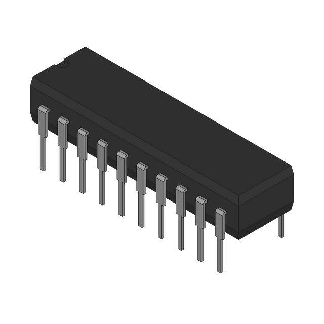
PIN CONNECTIONS
20-Pin Hermetic DIP (R-Suffix),
20-Pin Plastic DIP (P-Suffix),
20-Pin SOL (S-Suffix)
GENERAL DESCRIPTION
The DAC312 series of 12-bit multiplying digital-to-analog converters provide high speed with guaranteed performance to
0.012% differential nonlinearity over the full commercial operating temperature range.
The DAC312 combines a 9-bit master D/A converter with a
3-bit (MSBs) segment generator to form an accurate 12-bit D/A
converter at low cost. This technique guarantees a very uniform
step size (up to ± 1/2 LSB from the ideal), monotonicity to
12-bits and integral nonlinearity to 0.05% at its differential current outputs. In order to provide the same performance with a
12-bit R-2R ladder design, an integral nonlinearity over temperature of 1/2 LSB (0.012%) would be required.
The 250 ns settling time with low glitch energy and low power
consumption are achieved by careful attention to the circuit design and stringent process controls. Direct interface with all
popular logic families is achieved through the logic threshold
terminal.
High compliance and low drift characteristics (as low as
10 ppm/°C) are also features of the DAC312 along with an excellent power supply rejection ratio of ± .001% FS/%∆V. Operating over a power supply range of +5/–11 V to ± 18 V the
device consumes 225 mW at the lower supply voltages with an
absolute maximum dissipation of 375 mW at the higher supply
levels.
With their guaranteed specifications, single chip reliability and
low cost, the DAC312 device makes excellent building blocks
for A/D converters, data acquisition systems, video display drivers, programmable test equipment and other applications where
low power consumption and complete input/output versatility
are required.
FUNCTIONAL BLOCK DIAGRAM
REV. C
Information furnished by Analog Devices is believed to be accurate and
reliable. However, no responsibility is assumed by Analog Devices for its
use, nor for any infringements of patents or other rights of third parties
which may result from its use. No license is granted by implication or
otherwise under any patent or patent rights of Analog Devices.
© Analog Devices, Inc., 1996
One Technology Way, P.O. Box 9106, Norwood, MA 02062-9106, U.S.A.
Tel: 617/329-4700
Fax: 617/326-8703
�DAC312–SPECIFICATIONS
ELECTRICAL CHARACTERISTICS
Parameter
Symbol
Resolution
Monotonicity
Differential Nonlinearity
DNL
Nonlinearity
INL
Full-Scale Current
IFS
Full-Scale Tempco
TCI FS
Output Voltage Compliance
VOC
Full-Scale Symmetry
Zero-Scale Current
Settling Time
IFSS
IZS
tS
Propagation Delay–All Bits
tPLH
tPHL
Output Resistance
Output Capacitance
Logic Input
Levels “0”
Levels “1”
Logic Input Current
Logic Input Swing
Reference Bias Current
Reference Input
Slew Rate
Power Supply Sensitivity
RO
COUT
Power Supply Current
Power Dissipation
Conditions
DAC312E
Typ
Max
Min
Min
12
12
Deviation from Ideal
Step Size 2
Deviation from Ideal
Straight Line1
VREF = 10 V
R14 = R15 = 10 kΩ2
DNL Specification Guaranteed over Compliance Range
|IFS|–|IFS|
dl/dt
PSSI FS+
R14(eq) = 800 Ω, CC = 0 pF1
V+ = +13.5 V to +16.5 V,
V– = –15 V
V– = –13.5 V to –16.5 V,
V+ = +15 V
VOUT = 0 V
VOUT = 0 V
V+ = +5 V, V– = –15 V
V+ = +15 V, V– = –15 V
V+ = +5 V, V– = –15 V
V+ = +15 V, V– = –15 V
V+ = +5 V, V– = –15 V
V+ = +15 V, V– = –15 V
V+
V–
I+
I–
I+
I–
Pd
3.967
Units
12
12
Bits
Bits
± 0.0250 %FS
±1
LSB
± 0.05
%FS
± 0.0250
±1
± 0.05
4.031
± 20
± 0.002
3.935 3.999
± 10
± 0.001
4.063
± 40
± 0.004
3.935 3.999
± 80
± 0.008
4.063
mA
ppm/°C
%FS/°C
+10
±1
0.10
–5
± 0.4
+10
±2
0.10
–5
± 0.4
± 0.4
+10
±2
0.10
V
µA
µA
250
25
25
500
50
50
250
25
25
500
50
50
250
25
25
500
50
50
ns
ns
ns
>10
20
0.8
>10
20
0.8
2
–0.5
4
8
± 0.0005
40
+18
–2
2
–5
0
–0.5
4
8
± 0.001
± 0.0005
± 0.00025 ± 0.001
18
–10.8
3.3
7
–13.9
–18
3.9
7
–13.9
–18
225
305
267
375
4.5
–18
MΩ
pF
0.8
2
–5
0
TYPICAL ELECTRICAL CHARACTERISTICS
DAC312H
Typ
Max
3.999
±5
± 0.005
–5
4.5
–18
Min
12
12
>10
20
VLC = GND
VLC = GND
VIN = –5 to +18 V
DAC312F
Typ
Max
± 0.0125
± 0.5
± 0.05
To ± 1/2 LSB, All Bits
Switched ON or OFF1
All Bits Switched 50% Point
Logic Swing to 50% Point
Output1
VIL
VIH
IIN
VIS
I15
PSSIFS–
Power Supply Range
(@ VS = 615 V, IREF = 1.0 mA, 08C ≤ TA ≤ +708C for DAC312E and –408C ≤ TA ≤ +858C
for DAC312F, DAC312H, unless otherwise noted. Output characteristics refer
to both IOUT and IOUT.)
40
+18
–2
–5
0
–0.5
4
8
± 0.001
± 0.0005
± 0.00025 ± 0.001
18
–10.8
3.3
7
–13.9
–18
3.9
7
–13.9
–18
225
305
267
375
4.5
–18
40
+18
–2
V
V
µA
V
µA
mA/µs
± 0.001
%FS/%∆V
± 0.00025 ± 0.001
18
–10.8
3.3
7
–13 9
–18
3.9
7
–13.9
–18
225
305
267
375
%FS/%∆V
V
V
mA
mA
mA
mA
mW
mW
@ 258C; VS = 615 V, and IREF = 1.0 mA, unless otherwise noted. Output
characteristics refer to both IOUT and IOUT.
Parameter
Symbol
Reference Input
Slew Rate
dl/dt
Propagation Delay
tPLH, tPHL
Settling Time
tS
Full-Scale
DAC312N
Typical
DAC312G
Typical
Units
8
8
mA/µs
Any Bit
25
25
ns
To ± 1/2 LSB, All
Bits Switched ON
or OFF.
250
250
ns
± 10
± 10
ppm/°C
Conditions
TCIFS
–2–
REV. C
�DAC312
ELECTRICAL CHARACTERISTICS
@ VS = 615 V, IREF = 1.0 mA, 08C ≤ TA ≤ 708C for DAC312E and –408C ≤ TA ≤ +858C for
DAC312F, DAC312H, unless otherwise noted. Output characteristics refer to both IOUT and IOUT. Continued
Symbol
Conditions
Logic Input
Levels “0”
VIL
VLC = GND
Logic Input
Levels “1”
VIH
VLC = GND
Logic Input
Current
IIN
VIN = –5 V to +18 V
Logic Input
Swing
VIS
–5
Reference Bias
Current
I15
0
–0.5
4
8
Reference Input
Slew Rate
dl/dt
Power Supply
Sensitivity
PSSIFS+
PSSIFS–
Power Supply
Range
V+
V–
Power Supply
Current
I+
I–
I+
I–
Power
Dissipation
Pd
R14(eq) = 800 Ω
CC = 0 pF (Note 1)
Min
DAC312E
Typ
Max
Parameter
0.8
2
2
Max
Units
0.8
V
2
V
40
+18
–5
–2
0
–0.5
4
8
+18
–5
–2
0
–0.5
4
8
40
µA
+18
V
–2
µA
mA/µs
± 0.0005 ± 0.001
± 0.0005 ± 0.001
± 0.0005 ± 0.001 %FS/%∆V
± 0.00025 ± 0.001
± 0.00025 ± 0.001
± 0.00025 ± 0.001 %FS/%∆V
4.5
–18
18
–10.8
4.5
–18
18
–10.8
4.5
–18
18
–10.8
V+ = +5 V, V– = –15 V
V+ = +15 V, V– = –15 V
3.3
–13.9
3.9
–13.9
7
–18
7
–18
3.3
–13.9
3.9
–13.9
7
–18
7
–18
3.3
–13.9
3.9
–13.9
7
–18
7
–18
V+ = +5 V, V– = –15 V
V+ = +15 V, V– = –15 V
225
267
305
375
225
267
305
375
225
267
305
375
NOTES
1
Guaranteed by design.
2
TA = +25°C for DAC312H grade only.
Specifications subject to change without notice.
REV. C
DAC312H
Min Typ
0.8
40
V+ = +13.5 V to +16.5 V,
V– = –15 V
V– = –13.5 V to –16.5 V,
V+ = +15 V
VOUT = 0 V
DAC312F
Min Typ
Max
–3–
V
mA
mW
�DAC312
WAFER TEST LIMITS @ V = 615 V, I
S
REF =
1.0 mA, TA = 258C, unless otherwise noted. Output characteristics refer to both IOUT and IOUT.
DAC312N
Limit
DAC312G
Limit
Units
Resolution
12
12
Bits min
Monotonicity
12
12
Bits min
Parameter
Symbol
Conditions
± 0.05
± 0.05
%FS max
Full-Scale Current
Change 500 Ω.
Settling time and propagation delay are relatively insensitive to
logic input amplitude and rise and fall times, due to the high
gain of the logic switches. Settling time also remains essentially
constant for IREF values down to 0.5 mA, with gradual increases
for lower IREF values lies in the ability to attain a given output
level with lower load resistors, thus reducing the output RC
time constant.
Measurement of the settling time requires the ability to accurately resolve ± 1/2 LSB of current, which is ± 500 nA for 4 mA
FSR. In order to assure the measurement is of the actual settling
time and not the RC time of the output network, the resistive
termination on the output of the DAC must be 500 Ω or less.
This does, however, place certain limitations on the testing apparatus. At IREF values of less than 0.5 mA, it is difficult to prevent RC damping of the output and maintain adequate
sensitivity. Because the DAC312 has 8 equal current sources for
the 3 most significant bits, the major carry occurs at the code
change of 000111111111 to 111000000000. The worst case settling time occurs at the zero to full-scale transition and it requires 9.2 time constants for the DAC output to settle to within
± 1/2 LSB (0.0125%) of its final value.
The DAC312 switching transients or “glitches” are on the order
of 500 mV-ns. This is most evident when switching through the
major carry and may be further reduced by adding small capacitive loads at the output with a minor sacrifice in transition speeds.
Fastest operation can be obtained by using short leads, minimizing output capacitance and load resistor values, and by adequate
bypassing at the supply, reference, and VLC terminals. Supplies
do not require large electrolytic bypass capacitors as the supply
current drain is independent of input logic states; 0.1 µF capacitors at the supply pins provide full transient protection.
The temperature coefficient of the reference resistor R14 should
match and track that of the output resistor for minimum overall
REV. C
–11–
�DAC312
DIFFERENTIAL VS. INTEGRAL NONLINEARITY
Integral nonlinearity, for the purposes of the discussion, refers
to the “straightness”of the line drawn through the individual response points of a data converter. Differential nonlinearity, on
the other hand, refers to the deviation of the spacing of the adjacent points from a 1 LSB ideal spacing. Both may be expressed
as either a percentage of full-scale output or as fractional LSBs
or both. The following figures define the manner in which these
parameters are specified. The left figure shows a portion of the
transfer curve of a DAC with 1/2 LSB INL and the (implied)
DNL spec of 1 LSB. Below this is a graphic representation of
the way this would appear on a CRT, for example, if the D/A
converter output were to be applied to the Y input of a CRT as
shown in the application schematic titled “CRT Display Drive.”
On the right is a portion of the transfer curve of a DAC specified for 2 LSB INL with 1/2 LSB DNL specified and the
graphic display below it.
One of the characteristics of an R-2R DAC in standard form is
that any transition which causes a zero LSB change (i.e., the
same output for two different codes) will exhibit the same output each time that transition occurs. The same holds true for
transitions causing a 2 LSB change. These two problem transitions are allowable for the standard definition of monotonicity
and also allow the device to be specified very tightly for INL.
The major problem arising from this error type is in A/D converter implementations. Inputs producing the same output are
now represented by ambiguous output codes for an identical input. Also, 2 LSB gaps can cause large errors at those input levels (assuming 1/2 LSB quantizing levels). It can be seen from
the two figures that the DNL specified D/A converter will yield
much finer grained data than the INL specified part, thus improving the ability of the A/D to resolve changes in the analog
input.
DIFFERENTIAL LINEARITY COMPARISON
D/A Converter with ± 1/2 LSB INL, ± 1 LSB DNL
D/A Converter with ± 2 LSB INL, ± 1/2 LSB DNL
Video Deflection by DACs
Video Deflection by DACs
ENLARGED “POSITIONAL” OUTPUTS
ENLARGED “POSITIONAL” OUTPUTS
–12–
REV. C
�DAC312
DESCRIPTION OF OPERATION
The DAC312 is divided into two major sections, an 8 segment
generator and a 9-bit master/slave D/A converter. In operation
the device performs as follows (see Simplified Schematic).
The three most significant bits (MSBs) are inputs to a 3-to-8
line decoder. The selected resistor (R5 in the figure) is connected to the master/slave 9-bit D/A converter. All lower order
resistors (R1 through R4) are summed into the IO line, while all
higher order resistors (R6 through R8) are summed into the IO
line. The R5 current supplies 512 steps of current (0 mA to
0.499 mA for a 1 mA reference current) which are also summed
into the IO or IO lines depending on the bits selected. In the figure, the code selected is: 100 110000000. Therefore, 2 mA (4 ×
0.5 mA/segment) +0.375 mA (from master/slave D/A converter)
are summed into IO giving an IO of 2.375 mA. IO has a current
of 1.625 mA with this code. As the three MSB’s are incremented, each successively higher code adds 0.5 mA to IO and subtracts 0.5 mA from IO, with the selected resistor feeding its
current to the master/slave D/A converter; thus each increment
of the 3 MSBs allows the current in the 9-bit D/A converter to
be added to a pedestal consisting of the sum of all lower order
currents from the segment generator. This configuration guarantees monotonicity.
Expanded Transfer Characteristic Segment (001 010 011)
Simplified Schematic
REV. C
–13–
�000000000
12-Bit Fast A/D Converter
Outline Dimensions
Dimension shown in inches and (mm).
20-Lead Plastic DIP (N-20)
20-Lead Cerdip (Q-20)
PRINTED IN U.S.A.
20-Lead Wide Body SOL (R-20)
–14–
�Analog Products -- DAC312
Package/Price Information
For detailed packaging information, please select the Datasheets button.
12-Bit High Speed Multiplying D/A Converter
Status
Package
Description
DAC312BR
PRODUCTION
CERDIP GLASS SEAL
20
MILITARY
$29.65
DAC312BR/883C
PRODUCTION
CERDIP GLASS SEAL
20
MILITARY
$34.60
DAC312ER
PRODUCTION
CERDIP GLASS SEAL
20
INDUSTRIAL
$19.75
DAC312FR
PRODUCTION
CERDIP GLASS SEAL
20
INDUSTRIAL
$9.85
DAC312GBC
PRODUCTION
CHIPS/DIE SALES
TBD
$4.00
DAC312HP
PRODUCTION
PLASTIC/EPOXY DIP
20
COMMERCIAL
$4.50
DAC312HS
PRODUCTION
STD S.O. PKG (SOIC)
20
COMMERCIAL
$4.50
Model
Pin
Count
-
Temperature
Range
Price*
(100-499)
* This price is provided for budgetary purposes as recommended list price in U.S. Dollars per unit the
stated volume. Pricing displayed for Evaluation Boards and Kits is based on 1-piece pricing. View
Pricing and Availability (currently available to North American customers) for further information.
file:///F|/cpl_new_images/DAC312.html [7/18/2001 5:37:32 PM]
�