DEMO CIRCUIT 1562A
QUICKLTC699X
START GUIDE
LTC699X-X
TimerBlox: Oscillators,
One Shots, PWM, and Delay
DESCRIPTION
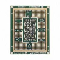
Demonstration circuit 1562A is an engineering tool
to design and evaluate the LTC699X-X family of
TimerBlox circuits. The center section of the board
contains a pre-configured TimerBlox function.
DC1562A comes in twelve timing function variations as outlined in Table 1.
Surrounding the center board is a ”playground”
prototyping area. The prototyping area has pads
for Dip-8, S8, MS8, or S6 packages with bread
boarding connections to each pin and two convenient power buses and ground bus surrounding the
entire area. This area is for conditioning signals to
control the timer function and for adding loads
controlled in time.
The center part of the board can be broken away
on its own as a convenience for adding a timing
function to a pre-existing circuit. For application
flexibility a provision is made for buffering and inverting the output of the timer. An optional
NC7W04P6X SC70 package dual inverter can be
added at U2 to provide this functionality.
Design files for this circuit board are available.
Call the LTC factory.
L, LTC, LTM, LT, Burst Mode, OPTI-LOOP, Over-The-Top and PolyPhase are
registered trademarks of Linear Technology Corporation. Adaptive Power, C-Load,
DirectSense, Easy Drive, FilterCAD, Hot Swap, LinearView, µModule, Micropower
SwitcherCAD, Multimode Dimming, No Latency ∆Σ, No Latency Delta-Sigma, No
RSENSE, Operational Filter, PanelProtect, PowerPath, PowerSOT, SmartStart,
SoftSpan, Stage Shedding, SwitcherCAD, ThinSOT, UltraFast and VLDO are trademarks of Linear Technology Corporation. Other product names may be trademarks
of the companies that manufacture the products.
USING THE DEMO BOARD
To understand the simplicity and flexibility of the
TimerBlox function download the appropriate datasheet from the LTC Website, www.linear.com for
the device to be used. To change the board from
the supplied default configuration is a simple matter of determining a few new resistor values. Simply select a pair of resistor values for the DIV value
from the data sheet DIV Table, calculate the value
of RSET required, replace the resistor on the board,
apply power, and go! Single supply power between
2.25V and 5.5V and ground must be supplied directly to the center board.
The outer prototyping section of the board can be
used with Single or Dual supplies as required.
When using the prototyping area, the outermost
trace, which is ground, must be connected (hand
wired) to the ground on the center board section.
All input and output holes are sized for 65 mil. turret terminals, or wires can be soldered in the holes
directly.
To experiment with different timer configurations
requires changing resistor values on the center
board. The through hole resistor lead holes can
take pressed in IC socket pins from DIP sockets or
resistors can soldered directly in the holes. Pads
for 0805 surface mount resistors are also included
at each position where a leaded resistor could be
used. Pads are also included for three 25-turn trim
1
�LTC699X
pots which can be used to replace RSET (R8) for
master oscillator frequency adjustment, PSF in
(R10) for voltage controlled options, and RDEV (R7)
for frequency divider control to permit real-time
adjustments while running.
A TimerBlox part, decoupling cap and a bulk decoupling 10µF Tantalum cap are already placed on
the board. Resistors are also provided to configure
each device for a representative function to start
evaluating these unique timing functions.
TABLE 1. STANDARD CONFIGURATION FOR EACH VERSION
Demo Board
Number
DC1562A-A
DC1562A-B
DC1562A-C
DC1562A-D
DC1562A-E
DC1562A-F
DC1562A-G
DC1562A-H
DC1562A-I
DC1562A-J
DC1562A-K
DC1562A-L
*
**
2
LTC Part
Number
LTC6990
LTC6991
LTC6992-1
LTC6992-2
LTC6992-3
LTC6992-4
LTC6993-1
LTC6993-2
LTC6993-3
LTC6993-4
LTC6994-1
LTC6994-2
Part
Marking
LTDWW
LTDWY
LTDXB
LTDXD
LTFCQ
LTFCS
LTDXG
LTDXJ
LTFMH
LTFMK
LTFCV
LTFCX
Rising Edge Triggered
Falling Edge Triggered
Function
Configured Function
HF OSC
LF OSC
PWM
PWM
PWM
PWM
One-Shot
One-Shot
One-Shot
One-Shot
Delay
Delay
1KHz to 10 KHz Voltage Controlled Oscillator
1 Hz ( 1Sec ) Fixed Frequency Oscillator
10KHz 0 – 100% Duty Cycle PWM
10KHz 5 – 95% Duty Cycle PWM
10KHz 0 – 95% Duty Cycle PWM
10KHz 5 – 100% Duty Cycle PWM
RET* 100 ms Positive Output Pulse
RET* Re-Triggerable 100 ms Positive Output Pulse
FET** Positive 100 ms Output Pulse
FET** Re-Triggerable 100 ms Positive Output Pulse
Output Falling Edge Delayed 100 ms from Input Falling Edge
Output Rise/Fall Edges Delayed 100 ms from Input Rise/Fall Edges
�LTC699X
DC1562A-X EXTERNAL CONNECTION DIAGRAM
3
�LTC699X
DC1562A-X CENTER BOARD CONNECTION DIAGRAM
4
�LTC699X
DEFAULT CIRCUIT CONFIGURATIONS FOR EACH VERSION
DC1652A-A, 1KHZ TO 10KHZ VCO
DC1652A-B, 1HZ (1SEC PERIOD) FIXED FREQUENCY OSCILLATOR
DC1652A-C, 10KHZ 0% TO 100% DUTY CYCLE PWM
5
�LTC699X
DEFAULT CIRCUIT CONFIGURATIONS FOR EACH VERSION
DC1652A-D, 10KHZ 5% TO 95% DUTY CYCLE PWM
DC1652A-E, 10KHZ 0% TO 95% DUTY CYCLE PWM
DC1652A-F, 10KHZ 5% TO 100% DUTY CYCLE PWM
6
�LTC699X
DEFAULT CIRCUIT CONFIGURATIONS FOR EACH VERSION
DC1652A-G, RISING EDGE TRIGGERED 100MS POSITIVE OUTPUT PULSE ONE SHOT
DC1562A-H, RISING EDGE RE-TRIGGERABLE 100MS POSITIVE OUTPUT PULSE ONE SHOT
DC1562A-I, FALLING EDGE TRIGGERED 100MS POSITIVE OUTPUT PULSE ONE SHOT
7
�LTC699X
DEFAULT CIRCUIT CONFIGURATIONS FOR EACH VERSION
DC1562A-J, FALLING EDGE RE-TRIGGERABLE 100MS POSITIVE OUTPUT PULSE ONE SHOT
DC1562A-K, 100MS DELAYED OUTPUT FALLING EDGE FROM INPUT FALLING EDGE
DC1562A-L, 100MS DELAYED OUTPUT EDGE FROM INPUT EDGE, BOTH RISING AND FALLING EDGES
8
�LTC699X
9
�