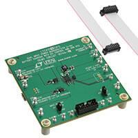
DEMO MANUAL DC1674A-B
LTC4156EUFD
Dual Input Power Manager/3.5A LiFePO4
Battery Charger with I2C Control and USB OTG
DESCRIPTION
Demonstration Circuit 1674A-B is dual input power
manager/3.5A LiFePO4 battery charger with I2C control
and USB On-The-Go (OTG).
Most functions on the LTC®4156EUFD are controlled via
the I2C serial interface. The LTC4156EUFD also provides
extensive status information via the I2C serial interface.
The dual input multiplexer, overvoltage protection (OVP)
and reverse voltage protection (RVP) is implemented with
external N-channel MOSFETs.
Please refer to the LTC4156EUFD data sheet for details
about the I2C serial interface, control and status registers,
and the electrical and timing specifications.
An on board buck regulator generates the VOUT voltage
from the active input voltage. This voltage is regulated to
minimize the dissipation in the battery charger. The minimum voltage of the VOUT regulator is 3.2V to provide an
instant-on function when the battery is fully discharged.
The LTC4156EUFD does modify several of its own control
registers to reflect the current operating conditions.
PERFORMANCE SUMMARY
(TA = 25°C)
SYMBOL
PARAMETER
CONDITIONS
VWALL
WALL Input Voltage Range
IWALL
Input Current from WALL Input
VUSB
USB Input Voltage Range
IUSB
Input Current from USB Input
Design files for this circuit board are available at
http://www.linear.com/demo
L, LT, LTC, LTM, μModule, Linear Technology and the Linear logo are registered trademarks
and QuikEval is a trademark of Linear Technology Corporation. All other trademarks are the
property of their respective owners.
4.35V < VWALL < 6V
4.35V < VUSB < 6V
VOUT
Voltage on the VOUT Pin
0A < IVOUT ≤ 4A, 2.7V < VBAT ≤ 3.8V
IVOUT
Output Current from VOUT
Total Load Current Including Battery Charger
VBAT
Voltage on the BAT Pin
IBAT
BAT Pin Source or Sink Current
VWALL,USB
Input Voltage Range, Non-Operating
MIN
TYP
MAX
4.35
5
5.5
UNITS
V
0
0.1
3
A
4.35
5
5.5
V
0
0.1
3
A
3.19
3.5
4.6
V
4.5
A
3.6
V
–4
3
A
5.75
27
V
3.3
Switching Regulator Efficiency
I2C Controlled High Power Battery Charger/USB Power Manager
VIN
VOUT
CHGSNS
VBUS
10μF
3.6k
2
LTC4156
USBGT
BATSNS
USBSNS
ID
I2C IRQ GND CLPROG2 CLPROG1 PROG VC
1.21k
499Ω
22μF
BATGATE
90
TO
SYSTEM
LOAD
100k
80
EFFICIENCY (%)
1μH
SW
WALLSNS
WALLGT
100
70
60
50
40
30
NTCBIAS
NTC
OVGCAP
20
10
0.1μF
VBAT = 3.3V
0
47nF
0
0.5
2.0
1.5
1.0
LOAD CURRENT (A)
2.5
3.0
DC1674ab TA01b
dc1674ab TA01a
dc1674abf
1
�DEMO MANUAL DC1674A-B
QUICK START PROCEDURE
DC1674A-B working input voltage range is 4.35V to 5.5V
on both the WALL and USB input. The DC1674A-B will
tolerate non-operating overvoltage inputs up to 27V.
DC1674A-B utilizes the DC590B, USB to I2C interface
board, to control the LTC4156EUFD and to read back the
contents of the command and status registers.
The DC1674A-B is easy to set up to evaluate the performance of the LTC4156EUFD. Refer to Figure 1 and Figure 2
for proper measurement equipment setup and follow the
evaluation procedure below using the DC590B board.
NOTE. When measuring the input or output voltage ripple,
care must be taken to avoid a long ground lead on the
oscilloscope probe. Measure the input or output voltage
ripple by touching the probe tip directly across the VIN or
VOUT and GND terminals. See Figure 2 for proper scope
probe technique.
Figure 1. Proper Measurement Equipment Setup
Figure 2. Measuring Input or Output Ripple
dc1674abf
2
�DEMO MANUAL DC1674A-B
QUICK START PROCEDURE
1. Ensure that JP1 and JP2 are in their default positions,
as shown in Figure 1. Set PS3 to 3.6V and turn on. The
DVCC voltage level may be selected on the DC590B.
This is done by setting the VCCIO jumper, JP6, on the
DC590B board to one of the following settings: 3.3V,
5V, removed for 2.7V or set to external if an external
supply is desired to be used. Please set DVCC to 3.3V.
2. Start the Linear Technology QuickEval™ program.
Download and install the latest version of the QuikEval
program from the following weblink: http://www.linear.
com/designtools/software/. This program should automatically detect the presence of the LTC4156EUFD
demo board (DC1674A-B) and activate the appropriate
GUI, as seen in Figure 3.
3. Set PS1 to 5V, and turn on. The “WALL Input Power
Available” and “External Power Available” indicators on
the GUI should turn green. The current on PS1 should
indicate approximately 80mA.
4. Set “WALL ILIM” to 3000mA. To compensate for the
sense resistance of IM1, adjust PS3 such that VM3
reads 3.6V. PS1 should now read approximately 2A,
and IM1 should read approximately 2.4A.
5. Set PS2 to 5V, and turn on. The only change should
be the “USB Input Power Available” indicator should
turn green.
6. Set the “USB ILIM” to 3000mA, and select the USB Input
radio button in the “Input Power Priority” frame. PS1
should now read 0A, PS2 should read approximately
2A, and IM1 should be unchanged at 2.4A
7. Set LD1 to 1A, and turn on. PS2 should now read approximately 3A, and IM1 should be unchanged.
8. Set “ICHARGE%” to 50%. PS2 should now read approximately 2A, and IM1 should be 1.2A.
USING THE LTC4156EUFD SOFTWARE
Introduction
The DC1674A-B GUI provides control of most aspects
of operation of the LTC4156EUFD. The DC1674A-B GUI
continuously reads back the LTC4156EUFD registers and
updates the displayed status accordingly. The DC1674A-B
GUI also provides a means to change the value of the
CLPROGx and PROG resistors, as well as the β of the NTC
device. The user is responsible for ensuring that these
values match the values on the physical Demo Board.
The DC1674A-B GUI will remember these values from
session to session, and they can be reset to the default
values at any time.
The DC1674A-B GUI is composed of three forms, the
LTC4156 form (Figure 3) that is brought up by the QuickEval program, the Manage Current Limit Resistors form
(Figure 4), that is brought up by pressing the “Change
Resistors” button on the LTC4156 form, and the Manage
β Value form (Figure 5) that is brought up by pressing the
“Change β” button on the LTC4156 form.
Any changes made in the Manage Current Limit Resistors
or Manage β Value forms will be reflected on the main form
as soon as “Apply” is pressed. All changes made in these
two forms will be remembered from session to session.
The values can be set to default at any time.
View LTC4156EUFD Product Page
This button opens your default internet browser, and
searches the Linear Technology Corporation web site for
information on the LTC4156EUFD when an internet connection is available.
WALL and USB ILIM Sections
9. Turn off and disconnect PS1, VM1, and PS2.
These sections allow control over the WALL and USB
input current limit.
10. Select the “Force OTG Boost On” radio button. VM2
should now read approximately 5V.
These sections should default to 100mA at power-up,
when the USB/USER (JP1) is in the “USB” position. They
dc1674abf
3
�DEMO MANUAL DC1674A-B
QUICK START PROCEDURE
should both default to the 1000mA value at the top of
the frame, at power-up, with the USB/USER (JP1) in the
“USER” position.
If the USB input power becomes unavailable, the USB ILIM
section will return to 100mA.
Input Power Priority
By default, the WALL input has priority on the input power
multiplexer. The priority can be reassigned to USB input
by selecting the appropriate radio button.
OTG Boost Automatic Enable
ICHARGE% Section
This section controls the battery charging current as a
percent of maximum. The maximum is shown at the top
of the frame, and is calculated from the displayed PROG
resistor value.
C/x Set
Select the End of Charging condition. This selects the
current, as a percent of the maximum that indicates end
of charging. Optionally, charging may also be terminated
at the C/x current threshold by selecting the “4hr or C/x”
timer mode.
Timer
This selects the timeout for the charging timer. When
the end of charging condition is reached, the charger is
not turned off, but the timer is started, and when it times
out, the charger is turned off. The exception is “4hr or
C/x” mode, where whichever 4hrs or C/x, occurs first will
terminate charging.
VFLOAT
This selects the desired battery float voltage, and defaults
to 3.45V.
Selectes whether or not the ID pin of the USB connector
enables USB On-The-Go (OTG) operation. It may be desirable to control USB OTG directly, without the need to set
the USB connector ID pin voltage level below VID_OTG. To
control USB OTG directly, check the “Force OTG Boost
On” box. Automatic enable has no effect on ID pin status
indication.
Disable Input UVCL
As the active input voltage (USB or WALL) drops below
4.3V, the LTC4156EUFD will lower the input current limit to
attempt to prevent the input voltage from drooping lower.
This is a useful feature in the input supply voltage is not
very stiff, or if there is significant impedance between the
input supply and the LTC4156EUFD. If this function is not
desired, check the “Disable Input UVCL” box.
Interrupts
The LTC4156EUFD can monitor a variety of conditions,
which it reports over the I2C buss. By selecting the check
boxes in the Interrupt section, the LTC4156EUFD can also
issue interrupts whenever one of these conditions changes.
The presence of an interrupt is indicated by the indicator
changing to red and displaying “Interrupt Pending.” The
interrupt can be cleared by pressing the “Clear Interrupt”
button. Changing the interrupt mask also clears all pending interrupts.
dc1674abf
4
�DEMO MANUAL DC1674A-B
QUICK START PROCEDURE
Figure 3. LTC4156 Main Form
Figure 4. Manage Current Limit Resistors Form
Figure 5. Manage β Value Form
dc1674abf
5
�DEMO MANUAL DC1674A-B
PARTS LIST
ITEM
QTY
REFERENCE
PART DESCRIPTION
MANUFACTURER/PART NUMBER
Capacitor, Chip, X5R, 22μF, ±10%, 25V, 1210
Murata, GRM32ER61E226KE15L
Required Circuit Components
1
2
C1, C2
2
3
C3, C11, C12
Capacitor, Chip, X5R, 22μF, ±20%, 6.3V, 0805
TAIYO-YUDEN, JMK212BJ226MG
3
1
C5
Capacitor, Chip, X7R, 0.01μF, ±10%, 25V, 0402
TDK, C1005X7R1E103K
4
1
C9
Capacitor, Chip, X7R, 0.047μF, ±10%, 25V, 0402
TDK, C1005X7R1E473K
5
1
C10
Capacitor, Chip, X5R, 100μF, ±20%, 6.3V, 1210
Murata, GRM32ER60J107ME20L
6
1
L1
Inductor, SMT, 1μH, 10.8mΩ, ±20%, 4mm × 4mm
Coilcraft, XFL4020-102ME
7
2
M1-M2
MOSFET, 40V, 25mΩ, 12A, Power33
Fairchild, FDMC8030
8
1
M3
MOSFET, –20V, 22mΩ, 12A, Power PAK ChipFET Single
Vishay, Si5481DU-T1-GE3
9
1
Q1, Q2
Dual NPN, SOT363
Diodes/Zetex, MMDT3904-7-F
10
2
R1, R5
Resistor, Chip, 1MΩ, ±5%, 1/16W, 0402
Vishay, CRCW04021M00JNED
11
2
R2, R6
Resistor, Chip, 3.6k, ±5%, 1/8W, 0805
Vishay, CRCW08053K60JNED
12
2
R3, R4
Resistor, Chip, 47k, ±5%, 1/16W, 0402
Vishay, CRCW040247K0JNED
13
2
R13, R17
Resistor, Chip, 100k, ±1%, 1/16W, 0402
Vishay, CRCW0402100KFKED
14
2
R14, R15
Resistor, Chip, 1.21k, ±1%, 1/16W, 0402
Vishay, CRCW04021K21FKED
15
1
R16
Resistor, Chip, 499Ω, ±1%, 1/16W, 0402
Vishay, CRCW0402499RFKED
16
4
R18, R19, R22, R23
Resistor, Chip, 0Ω Jumper, 1/16W, 0402
Vishay, CRCW04020000Z0ED
17
1
U1 (ASSEMBLY - A)
U1 (ASSEMBLY - B)
Dual Input Power Manager/3.5A Li-Ion Battery Charger
with I2C Control and USB OTG
Linear Technology, LTC4155EUFD
Linear Technology, LTC4156EUFD
Murata, GRM31CR71H475KA12L
Additional Demo Board Circuit Components
1
1
C4
Capacitor, Chip, X7R, 4.7μF, ±10%, 50V, 1206
2
1
C6
Capacitor, Chip, X7R, 0.01μF, ±10%, 25V, 0402
TDK, C1005X7R1E103K
3
1
C7
Capacitor, Chip, X5R, 0.1μF, ±10%, 25V, 0402
TDK, C1005X5R1E104K
4
0
C8-OPT
Capacitor, Chip, TBD, 0402
User Defined
5
0
C13-OPT
Capacitor, Chip, X5R, 22μF, ±10%, 25V, 1210
Murata, GRM32ER61E226KE15L
6
1
D1
LED, Red, 0603
Panasonic, LNJ208R8ARA
7
1
R7
Resistor, Chip, 1.0Ω, ±5%, 1/16W, 0402
Vishay, CRCW04021R00JNED
8
1
R8
Resistor, Chip, 100k, ±1%, 1/16W, 0402
Vishay, CRCW0402100KFKED
9
1
R9
Resistor, Chip, 0Ω Jumper, 1/16W, 0402
Vishay, CRCW04020000Z0ED
10
2
R10, R11
Resistor, Chip, 5.1k, ±5%, 1/16W, 0402
Vishay, CRCW04025K10JNED
11
1
R12
Resistor, Chip, 51k, ±5%, 1/16W, 0402
Vishay, CRCW040251K0JNED
12
1
R20
Resistor, Chip, 1k, ±5%, 1/10W, 0603
Vishay, CRCW06031K00JNED
13
0
R21-OPT
Resistor, Chip, TBD, 0402
User Defined
14
1
U2
I2C EEPROM
Microchip, 24LC025-I/ST
Turret, 0.09 DIA
Mill-Max, 2501-2-00-80-00-00-07-0
Hardware/Components (For Demo Board Only)
1
8
E1, E2, E3, E4, E11, E13, E14, E15
2
7
E5, E6, E7, E8, E9, E10, E12
Turret, 0.061 DIA
Mill-Max, 2308-2-00-80-00-00-07-0
3
1
J1
Connector, USB Micro-B
Tyco, 1981568-1
4
1
J2
Header, 2 × 7 Pin, 0.079CC
Molex, 87831-1420
5
0
J3-OPT
Connector, Battery
Hirose, DF3-3P-2DSA
6
2
JP1, JP2
Header, 3-Pin 1 Row 0.079CC
Samtec, TMM-103-02-L-S
7
2
JP1, JP2
Shunt, 2mm
Samtec, 2SN-KB-G
8
4
Stand-Off, Nylon, 0.375” Tall (Snap On)
Keystone, 8832 (SNAP ON)
9
1
FAB, Printed Circuit Board
Demo Circuit 1674A
10
2
Stencil - Top & Bottom
DC1674A-2
dc1674abf
6
�Information furnished by Linear Technology Corporation is believed to be accurate and reliable.
However, no responsibility is assumed for its use. Linear Technology Corporation makes no representation that the interconnection of its circuits as described herein will not infringe on existing patent rights.
A
B
C
USB
C1
22uF
1210
25V
E4
PROG
CLPROG2
CLPROG1
NTC
NTCBIAS
E9
E8
E7
E6
E5
1
3
5
7
9
11
13
+
+
+
+
+
+
+
J2
+
+
+
+
+
+
+
DC590
INTERFACE
GND
2
4
6
8
10
12
14
J1
MICRO-B
GND
D+
D-
ID
VBUS
5
R10
5.1k
5%
R8
100k
D+
TP1
DTP2
NON - OPERATING FAULT TOLERANCE TO
+ / - 27V CONTINUOUS.
4.35V - 5.5V
E3
GND
GND
GND
GND
GND
GND
D
E1
4.35V - 5.5V
E2
GND
WALL
NON - OPERATING FAULT TOLERANCE TO
+ / - 27V CONTINUOUS.
R7
1.0
5%
WP
24LC025I/ST
7
4
VSS
A0 256X8
A1
A2
1
2
3
8
VCC
SCLK
SDA 5
U2
C7
0.1μF
25V
Q2A
MMDT3904
Q2B
MMDT3904
R4
47k
5%
R3
47k
5%
6
C4
4.7uF
1206
50V
ID
TP3
C2
22uF
1210
25V
Q1B
MMDT3904
R11
5.1k
5%
0
R9
DVCC
4
1Meg
5%
R1
R6
R12
51k
5%
R14
1.21k
C6
0.01uF
25V
DVCC
TP14
FDMC8030
M1B
R15
1.21k
R16
499
3
SCL
TP16
OVGCAP
TP8
R17
100k
R18
0
USER
1
23
OVGCAP
USBGT
USBSNS
NTC
NTCBIAS
PROG
CLPROG2
CLPROG1
SCL
SDA
DVCC
ID
24
25
29
GND
SW 26
SW 27
IRQ
3
THIS CIRCUIT IS PROPRIETARY TO LINEAR TECHNOLOGY AND
SUPPLIED FOR USE WITH LINEAR TECHNOLOGY PARTS.
C9
0.047μF
25V
BATGATE
TP10
GEORGE B.
APP ENG.
2
SCALE = NONE
NC
PCB DES.
APPROVALS
BATSNS 16
VC 12
BATGATE 17
3
0
R23
L1
1.0μH
XFL4020-102ME
VOUTSNS
TP13
TP11
SW
2
DATE:
N/A
SIZE
LTC4156EUFD
-B
GEORGE B.
APPROVED
C12
22uF
0805
6.3V
20%
GND
R22
0
E10
E11
IRQ
GND
BATSNS
E12
BAT
E13
VFLOAT = 4.05V,
4.1V, 4.15V, 4.2V
4A
DF3-3P-2DSA
1 BAT J3
2 GND OPT
3 NTC
E14
VOUT
3.5V - 4.5V
4A
E15
DATE
05-05-11
05-05-11
IC NO.
1
LTC4155EUFD / LTC4156EUFD
DEMO CIRCUIT 1674A-A/B
SHEET 1
OF
1
2
REV.
DUAL INPUT POWER MANAGER / 3.5A Li-Ion
BATTERY CHARGER WITH I2C CONTROL AND USB OTG
1630 McCarthy Blvd.
Milpitas, CA 95035
Phone: (408)432-1900 www.linear.com
Fax: (408)434-0507
LTC Confidential-For Customer Use Only
R19
0
C10
100uF
6.3V
1210
20%
C13
22uF
1210
25V
20%
OPT
NOTES: UNLESS OTHERWISE SPECIFIED
1. RESISTORS: OHMS, 0402, 1%, 1/16W
2. CAPACITORS: uF, 0402, 10%, 50V
U1
LTC4155EUFD
-A
TECHNOLOGY
0603
R20
1k
5%
DVCC
TITLE: SCHEMATIC
C8
TBD
25V
OPT
R21
TBD
OPT
VC
TP9
1
ASSY
M3
Si5481DU
*
PRODUCTION FAB
DESCRIPTION
REVISION HISTORY
D1
LNJ208R8ARA
INTERRUPT
PENDING
RED
2
-
C11
22uF
0805
6.3V
20%
REV
ECO
LEAKAGE CURRENT MUST BE < 50nA
VOUT 22
VOUT 21
CHGSNS 20
CHGSNS 19
VOUTSNS 13
VBUS VBUS VBUS
WALLSNS
WALLGT
*
CUSTOMER NOTICE
NTC
3
EXT
15
14
18
6
5
28
1
2
4
10
9
8
7
11
U1
VBUS
TP12
LINEAR TECHNOLOGY HAS MADE A BEST EFFORT TO DESIGN A
CIRCUIT THAT MEETS CUSTOMER-SUPPLIED SPECIFICATIONS;
HOWEVER, IT REMAINS THE CUSTOMER'S RESPONSIBILITY TO
VERIFY PROPER AND RELIABLE OPERATION IN THE ACTUAL
APPLICATION. COMPONENT SUBSTITUTION AND PRINTED
CIRCUIT BOARD LAYOUT MAY SIGNIFICANTLY AFFECT CIRCUIT
PERFORMANCE OR RELIABILITY. CONTACT LINEAR
TECHNOLOGY APPLICATIONS ENGINEERING FOR ASSISTANCE.
JP2
1
INT
R13
100k
USB
3
JP1
C5
0.01μF
25V
U1.7,9,10 : LEAKAGE CURRENT
MUST BE < 400nA
C3
22uF
0805
6.3V
20%
TP4
WALLSNS
TP5
WALLGT
R2
3.6k
5%
0805
INPUT CURRENT
SDA
TP15
USBGT
TP6
M2A
FDMC8030
USBSNS
TP7
5%
R5
1Meg
M2B
FDMC8030
FDMC8030
M1A
3.6k
5%
0805
4
2
Q1A
MMDT3904
2
5
A
B
C
D
DEMO MANUAL DC1674A-B
SCHEMATIC DIAGRAM
dc1674abf
7
�DEMO MANUAL DC1674A-B
DEMONSTRATION BOARD IMPORTANT NOTICE
Linear Technology Corporation (LTC) provides the enclosed product(s) under the following AS IS conditions:
This demonstration board (DEMO BOARD) kit being sold or provided by Linear Technology is intended for use for ENGINEERING DEVELOPMENT
OR EVALUATION PURPOSES ONLY and is not provided by LTC for commercial use. As such, the DEMO BOARD herein may not be complete
in terms of required design-, marketing-, and/or manufacturing-related protective considerations, including but not limited to product safety
measures typically found in finished commercial goods. As a prototype, this product does not fall within the scope of the European Union
directive on electromagnetic compatibility and therefore may or may not meet the technical requirements of the directive, or other regulations.
If this evaluation kit does not meet the specifications recited in the DEMO BOARD manual the kit may be returned within 30 days from the date
of delivery for a full refund. THE FOREGOING WARRANTY IS THE EXCLUSIVE WARRANTY MADE BY THE SELLER TO BUYER AND IS IN LIEU
OF ALL OTHER WARRANTIES, EXPRESSED, IMPLIED, OR STATUTORY, INCLUDING ANY WARRANTY OF MERCHANTABILITY OR FITNESS
FOR ANY PARTICULAR PURPOSE. EXCEPT TO THE EXTENT OF THIS INDEMNITY, NEITHER PARTY SHALL BE LIABLE TO THE OTHER FOR
ANY INDIRECT, SPECIAL, INCIDENTAL, OR CONSEQUENTIAL DAMAGES.
The user assumes all responsibility and liability for proper and safe handling of the goods. Further, the user releases LTC from all claims
arising from the handling or use of the goods. Due to the open construction of the product, it is the user’s responsibility to take any and all
appropriate precautions with regard to electrostatic discharge. Also be aware that the products herein may not be regulatory compliant or
agency certified (FCC, UL, CE, etc.).
No License is granted under any patent right or other intellectual property whatsoever. LTC assumes no liability for applications assistance,
customer product design, software performance, or infringement of patents or any other intellectual property rights of any kind.
LTC currently services a variety of customers for products around the world, and therefore this transaction is not exclusive.
Please read the DEMO BOARD manual prior to handling the product. Persons handling this product must have electronics training and
observe good laboratory practice standards. Common sense is encouraged.
This notice contains important safety information about temperatures and voltages. For further safety concerns, please contact a LTC application engineer.
Mailing Address:
Linear Technology
1630 McCarthy Blvd.
Milpitas, CA 95035
Copyright © 2004, Linear Technology Corporation
dc1674abf
8
Linear Technology Corporation
LT 0312 • PRINTED IN USA
1630 McCarthy Blvd., Milpitas, CA 95035-7417
(408) 432-1900
●
FAX: (408) 434-0507 ● www.linear.com
© LINEAR TECHNOLOGY CORPORATION 2012
�