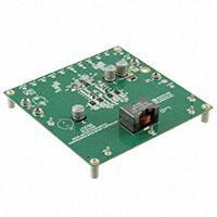
DEMO MANUAL DC2123A
LT3790
60V Four-Switch Synchronous
Buck-Boost Controller
DESCRIPTION
The DC2123A is a 60V four-switch synchronous buck-boost
controller that demonstrates the high power capability
of the LT®3790. The output is 24V and the maximum
output current is 5A. The switching frequency is 200kHz
and efficiency is as high as 98% for a 24V input.
The LT3790 is capable of high power operation. DC2123A
can be altered for either lower input voltage operation with
the same output power or for increased output power
with higher minimum input voltage. VIN can be reduced to
8VIN minimum and still deliver 120W output by changing
RS1 to 2mΩ, RIN1 to 1.5mΩ, and R3 (UVLO) to 88.7k. If
VIN remains always above 20V, IOUT can be increased to
12A+ (for 290W output) with the above changes, and an
additional change of ROUT to 4mΩ.
The operating input voltage range of DC2123A is from
12V to 57V. The output voltage, EN/UVLO, and OVLO are
all programmed by resistor dividers. EN/UVLO is set so
the circuit will turn off when the input voltage falls below
11.9V and will turn on when the input voltage rises above
13.4V. OVLO is set to engage for input voltages above 57V.
Current sense resistors program input and output current
limits and also determine the monitoring voltages that
indicate input and output current. IVINMON provides a
60mV/1A voltage that is used to monitor the input current. Input current limit occurs at 16.7A and is set by
RIN1. ISMON provides a 160mV/1A voltage that is used
to monitor the output current. The output current limit is
7.5A and is set by RS2.
The demo circuit features MOSFETs that compliment the
5V gate drive of the LT3790 to achieve high efficiency. 60V
MOSFETs are used on the input side of the four-switch
topology while 40V MOSFETs are used on the output side.
Ceramic capacitors are used at both the circuit input and
output because of their small size and high ripple current
capability. In addition to ceramic capacitors, there is an
aluminum polymer capacitor on the output that assures
feedback loop stability, even at low temperatures. The
input has an aluminum electrolytic capacitor in addition
to ceramic capacitors. A two-stage L-C input filter can
easily be added for electro-magnetic compatibility. The
pcb has large copper planes and extensive vias for thermal
performance.
The CLKOUT output and the SYNC input can be used to
synchronize switching between two or more DC2123A
circuits. A resistor from SYNC to ground must be removed
prior to using the SYNC input.
SHORT and C/10 are open-collector status flag outputs and
are pulled up to the INTVCC pin voltage. A resistor shorts
the CCM pin to C/10 and causes the circuit to change to
discontinuous conduction mode (DCM) when C/10 is active
at light load currents. CCM can also be connected with a
resistor to INTVCC instead of C/10 for continuous conduction mode (CCM) operation over the entire load range.
The CTRL input is pulled up to the VREF pin through a 0Ω
resistor to set the output current limit to its maximum,
and an external voltage on CTRL can be used to lower the
current limit if the resistor is removed. A capacitor at the
SS pin programs soft-start and additionally SS is pulled
up to the VREF pin through a 100k resistor. The switching
frequency is adjustable with a resistor.
The demo circuit is designed to be easily reconfigured to
many other applications, including the example schematics in the data sheet. Consult the factory for assistance.
High power operation, four-switch buck-boost topology,
fault protection and full monitoring make the LT3790
attractive for high power voltage regulator circuits and
also circuits that require output current regulation such
as battery chargers. The LT3790EFE is available in a
thermally enhanced 38-lead TSSOP package. The LT3790
data sheet must be read in conjunction with this demo
manual to properly use or modify demo circuit DC2123A.
Design files for this circuit board are available at
http://www.linear.com/demo/DC2123A
L, LT, LTC, LTM, Linear Technology and the Linear logo are registered trademarks of Linear
Technology Corporation. All other trademarks are the property of their respective owners.
dc2123af
1
�DEMO MANUAL DC2123A
PERFORMANCE SUMMARY
Specifications are at TA = 25°C
PARAMETER
CONDITIONS
Minimum Input Voltage, VPVIN
VOUT = 24V IOUT ≤ 4.5A
Maximum Input Voltage, VPVIN
VOUT = 24V IOUT ≤ 5A
Maximum Output Current
13.3V < VPVIN < 57V, CTRL = VREF
VPVIN = 12V, CTRL = VREF
Input EN Voltage, VPVIN(EN)
R3 = 56.2k, R4 = 499k, VPVIN Rising
13.4
V
Input UVLO Voltage, VPVIN(UVLO)
R3 = 56.2k, R4 = 499k, VPVIN Falling
11.9
V
Input OVLO Turn-Off Voltage, VPVIN(OVLO turn-off)
R11 = 27.4k, R1 = 499k, VPVIN Rising
57.6
V
Input OVLO Turn-On Voltage, VPVIN(OVLO turn-on)
R11 = 27.4k, R1 = 499k, VPVIN Falling
56.2
V
Output Voltage VOUT
R19 = 71.5k, R34 = 1.37k, R20 = 3.83k
Efficiency
VPVIN = 24V, IOUT = 5A
98
%
Switching Frequency
R18 = 147k
200
kHz
Input Current Limit
RIN1 = 0.003Ω
16.7
A
Output Current Limit
RS2 = 0.008Ω
7.5
A
MIN
TYP
MAX
UNITS
12
V
57
V
5
4.5
A
A
23.5
24.5
V
QUICK START PROCEDURE
It is easy to set up demonstration circuit DC2123A to
evaluate the performance of the LT3790. Refer to Figure 1
for the proper measurement equipment setup and follow
the procedure below:
NOTE: Make sure that the voltage applied to PVIN does
not exceed the absolute maximum voltage rating of 60V
for the LT3790.
1. Connect the EN/UVLO terminal to ground with a clip-on
lead. Connect the power supply (with power off), load,
and meters as shown.
2
2. After all connections are made, turn on the input power
and verify that the input voltage is between 12V and 57V.
3. Remove the clip-on lead from EN/UVLO. Verify that the
output voltage is 24V.
NOTE: If the output voltage is low, temporarily disconnect
the load to make sure that it is not set too high.
4. Once the proper output voltage is established, adjust
the input voltage and load within the operating ranges
and observe the output voltage regulation, ripple voltage, efficiency and other parameters.
dc2123af
�DEMO MANUAL DC2123A
QUICK START PROCEDURE
Figure 1. Proper Measurement Equipment Setup for DC2123A
100
VIN = 24V
VIN = 12V
EFFICIENCY (%)
95
90
85
80
0
1
3
2
LOAD CURRENT (A)
4
5
dc2123a F02
Figure 2. Efficiency
dc2123af
3
�DEMO MANUAL DC2123A
QUICK START PROCEDURE
VIN = 14V
VIN = 24V
VIN = 54V
Figure 3. Output Voltage Ripple at 5A Output Current, VOUT = 24V, 25MHz Bandwidth
VIN = 14V
VIN = 24V
VIN = 54V
Figure 4. Output Voltage Load Transient Response, VOUT = 24V, IOUT = 2.5A to 5A to 2.5A, 25MHz Bandwidth
4
dc2123af
�DEMO MANUAL DC2123A
QUICK START PROCEDURE
30
25
VOUT (V)
20
15
10
5
0
0
1
2
3
4
5
IOUT (A)
6
7
8
dc2009a F05
Figure 5. VOUT in Current Limit, VIN = 24V
DIFFERENCES BETWEEN LT3790 AND LT3791-1
The LT3790 is an improved version of the LT3791-1 and
is recommended for use in new designs. Some external
component values may change, but otherwise, the LT3790
is functionally equivalent to the LT3791-1. The differences
between the two products are:
1. The LT3790 has a 60mV (typical) full-scale V(ISP-ISN)
current sense voltage, compared to 100mV (typical) for
the LT3791-1. This change allows lower power current
sense resistors to be used for most applications.
2. The LT3790 CTRL pin linear range is from 0V to 1.1V,
and has a turn-off threshold of 50mV(typical), compared
to a 200mV to 1.1V linear range and 175mV (typical)
turn-off threshold for the LT3791-1. These changes
make it easier to parallel two or more LT3790 ICs for
higher power levels.
3. The LT3790 C/10 pin pulls low when the V(ISP-ISN) voltage
is less than 1/10 full scale, compared to the LT3791-1,
where C/10 pulls low when both V(ISP-ISN) is less than
1/10 full scale and VFB is greater than 1.15V(typical).
Since the C/10 pin is used to allow DCM mode for some
applications, this change ensures that negative current
does not occur at light loads for a broader range of
applications.
dc2123af
5
�DEMO MANUAL DC2123A
PARTS LIST
ITEM
QTY
REFERENCE
PART DESCRIPTION
MANUFACTURER/PART NUMBER
Required Electrical Components
1
1
CC1
Cap., X7R 0.01µF 25V 10% 0603
AVX 06033C103KAT2A
2
1
CC2
Cap., NPO 1000pF 25V 10% 0603
AVX 06033A102KAT1A
3
1
CSS1
Cap., X7R 33nF 25V 10% 0603
AVX 06033C333KAT1A
4
1
C1
Cap., X5R 0.47µF 16V 20% 0402
TDK C1005X5R1C474MT
5
3
C2, C12, C13
Cap., X5R 0.1µF 16V 10% 0402
TDK C1005X5R1C104KT
6
1
C3
Cap., X5R 1µF 100V 10% 1206
Taiyo Yuden HMK316BJ105KL-T
7
1
C4
Cap., X5R 4.7µF 10V 10% 0603
Taiyo Yuden LMK107BJ475KA
8
2
C6, C7
Cap., X7S 4.7µF 100V 10% 1210
TDK C3225X7S2A475K200AB
9
1
C10
Cap., Alum. Elect. 47µF 80V ± 20%
United Chemi-Con
EMZA800ADA470MJA0G
10
2
C14, C15
Cap., X5R 4.7µF 50V 20% 1210
Taiyo Yuden UMK325BJ475MM-T
11
2
C20, C30
Cap., Hybrid Cond. Polymer 220µF 35V 20%
SUN Electronic Industries 35HVP220M
12
1
C29
Cap., X7R 0.033µF 16V 10% 0402
TDK C1005X7R1C333K
13
2
D1, D2
Schottky Barrier 100V SOD323 (SC-90)
NXP Semi. BAT46WJ
14
1
L1
Inductor, 10µH SER2900
Coilcraft SER2918H-103KL
15
2
M1, M2
Mosfet-N Channel, 60V/25A LFPAK
Renesas RJK0651DPB-00-J5
16
2
M3, M4
Mosfet-N Channel, 40V/35A LFPAK
Renesas RJK0451DPB-00-J5
17
1
RC1
Res., Chip 15k 0.06W 5% 0402
Vishay CRCW040215K0JNED
18
1
RIN1
Res., 0.003 1W 1% 2512
Vishay WSL25123L000FEA
19
1
RS1
Res., 0.004 1/2W 1% 2010
Vishay WSL20104L000FEA
20
1
RS2
Res., 0.008 1W 1% 2512
Panasonic ERJ-M1WSF8M0U
21
2
R1, R4
Res., Chip 499k 0.06W 1% 0603
Vishay CRCW0603499KFKEA
22
1
R3
Res., Chip 56.2k 0.06W 1% 0402
Vishay CRCW040256K2FKED
23
1
R5
Res., Chip 51 0.06W 5% 0402
NIC NRC04F51R0TRF
24
2
R6, R10
Res., Chip 200k 0.06W 5% 0603
Vishay CRCW0603200KJNEA
25
1
R11
Res., Chip 27.4k 0.06W 1% 0402
Vishay CRCW040227K4FKED
26
1
R16
Res., Chip 200k 0.06W 5% 0402
Vishay CRCW0402200KJNED
27
1
R17
Res., Chip 100k 0.06W 5% 0402
Vishay CRCW0402100KJNED
28
1
R18
Res., Chip 147k 0.06W 1% 0402
Vishay CRCW0402147KFKED
29
1
R19
Res., Chip 71.5k 0.06W 1% 0603
Vishay CRCW060371K5FKEA
30
1
R20
Res., Chip 3.83k 0.06W 1% 0402
Vishay CRCW04023K83FKED
31
1
U1
I.C., 60V Buck-Boost Volt. Reg.
Linear Tech. Corp. LT3790EFE#PBF
6
dc2123af
�DEMO MANUAL DC2123A
PARTS LIST
ITEM
QTY
REFERENCE
PART DESCRIPTION
MANUFACTURER/PART NUMBER
Optional Electrical Components
1
0
C5, C8, C9, C16, C17, C18 (Opt)
Cap., 1210
2
0
C11, C19 (Opt)
OPTIONAL
3
0
C21, C22, C28
Cap., 0603
4
0
C23
OPTIONAL
5
0
C24, C25, C26, C27 (Opt)
OPTIONAL
6
0
D3, D4 (Opt)
Schottky Diode, SMB
7
0
D5, D6 (Opt)
Diode, SOD-123
8
0
D7 (Opt)
Diode, SOD-523
9
0
L2, L3 (Opt)
OPTIONAL
10
0
M5, M6, M7, M8, M12 (Opt)
OPTIONAL
11
0
M9, M10, M11 (Opt)
OPTIONAL
12
0
R2, R23, R24, R26-R32
Res., 0603 OPTIONAL
13
1
R7
Res.,Chip 0Ω 1206
14
0
R8, R9, R25
Res., 0402 OPTIONAL
15
3
R12, R14, R22
Res., Chip 0Ω 0402
Vishay CRCW04020000Z0ED
16
2
R13, R21
Res., Chip 0Ω 0603
Vishay CRCW06030000Z0EA
17
1
R34
Res., Chip 1.37k 0.06W 1% 0603
Panasonic ERJ-3EKF1371V
1
4
E1, E2, E19, E20
Connector, Banana Jack
Keystone 575-4
2
13
E3, E5, E6, E7, E8, E9, E10, E11, E12,
E13, E14, E21, E22
Turret, Testpoint
Mill Max 2308-2-00-80-00-00-07-0
3
5
E4, E15, E16, E17, E24
Turret, Testpoint
Mill Max 2501-2-00-80-00-00-07-0
4
0
E18 (Opt)
OPTIONAL
5
0
E23 (Opt)
OPTIONAL
6
4
MH1-MH4
Standoff Nylon 0.50"
Yageo RC1206FR-070RL
Hardware
Keystone, 8833 (Snap-On)
dc2123af
7
�E10
E9
E8
E7
E6
E5
E4
E3
GND
GND
GND
GND
R6
200k
5%
0603
INTVCC
VIN
R13
0 Ohm
0603
TP2
TP1
TP6
R10
200k
5%
0603
R8
(Opt)
TP5
R1
499k
0603
PVIN
VREF
INTVCC
*C/10
*SHORT
R3
56.2k
R2
(Opt)
0603
ALL RESISTORS 0402 1%.
ALL CAPACITORS 0603.
NOTE: UNLESS OTHERWISE SPECIFIED.
E17
E16
E15
E14
E11
ISMON
E12
CLKOUT
E13
SYNC
IVINMON
C/10
SHORT
CTRL
OVLO
EN/UVLO
GND
VIN
12V - 57V
E2
R16
100k
5%
R17
200k
5%
SS
2
C29
0.033µF
0402
32
34
33
7
8
4
5
6
1
38
VREF
CSS1
33nF
R14
0 Ohm
C2
0.1µF
0402
R12
0 Ohm
R11
27.4k
R9
(Opt)
9
R4
499K
0603
R18
147k
200kHz
SS
CCM
SYNC
CLKOUT
ISMON
0402
0.47µF
C1
0.003
1%
2512
R5
51
5%
U1
LT3790EFE
IVINMON
C/10
SHORT
VREF
CTRL
OVLO
EN/UVLO
RT
35
GND
RIN1
36
CC1
0.01µF
RC1
15k
5%
VC
PVIN
10
IVINP
11
IVINN
TEST1
29
E1
CC2
1000pF
TP4
TP3
PWM
PWMOUT
ISN
ISP
FB
TG2
SW2
BG2
SNSN
SNSP
BG1
SW1
TG1
BST2
BST1
SW1
16
SW2
TG2
FB
21
24
37
PWMOUT
PWM
31
3
26
25
BG2
RS1
0.004
1%
2010
SNSP
19
28
27
BG1
0 Ohm
0603
R21
M2
RJK0651DPB
TG1
18
C4
4.7µF
10V
M1
RJK0651DPB
INTVCC
14
22
15
13
C3
1µF
100V
1206
INTVCC
R7
0 Ohm
1206
VIN
12
SGND
SGND
30
39
PGND
PGND
8
20
17
PVIN
12V - 57V
INTVCC
D2
BAT46WJ
C6
4.7uF
100V
1210
D3
(Opt)
SMB
2
3
1
C13
0.1µF
L1 0402
10µH
SER2918H-103KL
C12
0.1µF
0402
D1
BAT46WJ
C5
(Opt)
1210
D4
(Opt)
SMB
C15
4.7µF
50V
1210
C9
(Opt)
1210
M4
RJK0451DPB
ISP
C14
4.7µF
50V
1210
C8
(Opt)
1210
M3
RJK0451DPB
C7
4.7uF
100V
1210
C16
(Opt)
1210
80V
C10
+ 47µF
(Opt)
C21
2512
0.008
RS2
C17
(Opt)
1210
R22
0 Ohm
C18
(Opt)
1210
(Opt)
12.5mm Dia.
Thru‐Hole
+ C11
IVINN
R20
3.83k
R19
71.5k
0603
R34
1.37k
0603
+ C20
(Opt)
220µF
12.5mm Dia.
35V
Thru‐Hole
+ C19
VOUT
E20
E19
220µF
35V
+ C30
OUT
GND
*SHORT
SS
VREF
*C/10
PWMOUT
FB
BG2
SW2
TG2
SNSP
BG1
SW1
TG1
ISP
PWM
INTVCC
VOUT
24V 5A
E18
(Opt)
DEMO MANUAL DC2123A
SCHEMATIC DIAGRAM
dc2123af
�PWM
Information furnished by Linear Technology Corporation is believed to be accurate and reliable.
However, no responsibility is assumed for its use. Linear Technology Corporation makes no representation that the interconnection of its circuits as described herein will not infringe on existing patent rights.
D5
C24
4.7µF
100V
1210
(Opt)
(Opt)
SOD-123
D6
(Opt)
SOD-123
PWM
C23
+ 47µF
80V
(Opt)
PVIN
E21
VIN
M9
(Opt)
SOT-23
FB
L2
4.7µH
R25
(Opt)
R26
(Opt)
0603
VREF
ISP
R24
D7
(Opt)
SOD-523
*SHORT
M6
(Opt)
LFPAK
L3
4.7µH
SNSP
SW1
SW1
M5
(Opt)
LFPAK
7443551470
C27 Wurth Electronik
4.7µF
(Opt)
100V
1210
(Opt)
PVIN
R28
(Opt)
0603
(Opt)
0603
R23
(Opt)
0603
C26
4.7µF
100V
1210
(Opt)
C22
(Opt)
R27
(Opt)
0603
BG1
*C/10
7443551470
C25 Wurth Electronik
4.7µF
(Opt)
100V
1210
(Opt)
ISP
IVINN
TG1
IVINN
PVIN
C28
(Opt)
R32
(Opt)
0603
SS
M10
(Opt)
SOT-23
R31
(Opt)
0603
VREF
BG2
TG2
R29
(Opt)
0603
R30
(Opt)
0603
PWMOUT
SNSP
SW2
SW2
ISP
M7
(Opt)
LFPAK
M8
(Opt)
LFPAK
M11
(Opt)
SOT-23
INTVCC
M12
(Opt)
LFPAK
INTVCC
*SHORT
SS
VREF
*C/10
PWMOUT
FB
BG2
SW2
TG2
SNSP
BG1
SW1
TG1
ISP
PWM
E24
(Opt)
E23
GND
LED-
E22
INTVCC
DEMO MANUAL DC2123A
SCHEMATIC DIAGRAM
10mm Dia. Surface Mount
dc2123af
9
�DEMO MANUAL DC2123A
DEMONSTRATION BOARD IMPORTANT NOTICE
Linear Technology Corporation (LTC) provides the enclosed product(s) under the following AS IS conditions:
This demonstration board (DEMO BOARD) kit being sold or provided by Linear Technology is intended for use for ENGINEERING DEVELOPMENT
OR EVALUATION PURPOSES ONLY and is not provided by LTC for commercial use. As such, the DEMO BOARD herein may not be complete
in terms of required design-, marketing-, and/or manufacturing-related protective considerations, including but not limited to product safety
measures typically found in finished commercial goods. As a prototype, this product does not fall within the scope of the European Union
directive on electromagnetic compatibility and therefore may or may not meet the technical requirements of the directive, or other regulations.
If this evaluation kit does not meet the specifications recited in the DEMO BOARD manual the kit may be returned within 30 days from the date
of delivery for a full refund. THE FOREGOING WARRANTY IS THE EXCLUSIVE WARRANTY MADE BY THE SELLER TO BUYER AND IS IN LIEU
OF ALL OTHER WARRANTIES, EXPRESSED, IMPLIED, OR STATUTORY, INCLUDING ANY WARRANTY OF MERCHANTABILITY OR FITNESS
FOR ANY PARTICULAR PURPOSE. EXCEPT TO THE EXTENT OF THIS INDEMNITY, NEITHER PARTY SHALL BE LIABLE TO THE OTHER FOR
ANY INDIRECT, SPECIAL, INCIDENTAL, OR CONSEQUENTIAL DAMAGES.
The user assumes all responsibility and liability for proper and safe handling of the goods. Further, the user releases LTC from all claims
arising from the handling or use of the goods. Due to the open construction of the product, it is the user’s responsibility to take any and all
appropriate precautions with regard to electrostatic discharge. Also be aware that the products herein may not be regulatory compliant or
agency certified (FCC, UL, CE, etc.).
No License is granted under any patent right or other intellectual property whatsoever. LTC assumes no liability for applications assistance,
customer product design, software performance, or infringement of patents or any other intellectual property rights of any kind.
LTC currently services a variety of customers for products around the world, and therefore this transaction is not exclusive.
Please read the DEMO BOARD manual prior to handling the product. Persons handling this product must have electronics training and
observe good laboratory practice standards. Common sense is encouraged.
This notice contains important safety information about temperatures and voltages. For further safety concerns, please contact a LTC application
engineer.
Mailing Address:
Linear Technology
1630 McCarthy Blvd.
Milpitas, CA 95035
Copyright © 2004, Linear Technology Corporation
10 Linear Technology Corporation
dc2123af
LT 1214 • PRINTED IN USA
1630 McCarthy Blvd., Milpitas, CA 95035-7417
(408) 432-1900
●
FAX: (408) 434-0507 ● www.linear.com
LINEAR TECHNOLOGY CORPORATION 2014
�