DEMO MANUAL DC890B
DC890B QuickStart Guide
DESCRIPTION
Demonstration circuit DC890B along with PScope™ software provides a USB based Windows PC hosted digital
data acquisition system supporting CMOS/LVDS output
ADCs up to 250Msps. The DC890B must be powered from
an external 6VDC ±0.5VDC power supply when operating in LVDS mode. When operating in CMOS mode, the
external power supply is optional. The Linear Technology
supplied PScope evaluation software automatically detects
the DC890B and can also detect many of the standard
ADC demonstration circuits boards. The DC890B will
not enable LVDS mode unless an external 6.0VDC power
source is available. This system provides for fast and easy
performance evaluation of high speed ADCs. DC890B
collects up to 256K word samples and then performs
various analyses on the data including calculating SNR,
SINAD, THD, SFDR and ENOB. The digitized input, an FFT
of the collected data, the primitive wave of the sample set
or an IFFT of modified frequency domain data is plotted to
a display window to facilitate analyzing distortion products
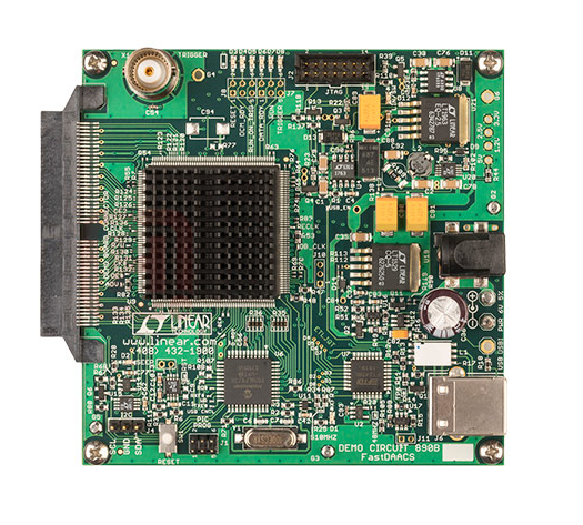
and sources. Figure 1 shows a picture of the DC890B. The
DC890B is connected to the ADC demonstration circuit via
a 100-pin edge connector, to the PC by a USB A-B cable and
to an optional power supply either by a 5mm power plug
or optionally by turrets. Figure 2 details the connections.
Design files for this circuit board are available at
http://www.linear.com/demo
L, LT, LTC, LTM, Linear Technology and the Linear logo are registered trademarks and PScope
is a trademark of Linear Technology Corporation. All other trademarks are the property of their
respective owners.
BOARD PHOTO
Figure 1. DC890B Board
dc890bf
1
�DEMO MANUAL DC890B
OPERATING PRINCIPLES
The DC890B is capable of collecting a block of data samples
from an ADC demonstration circuit initiated either by an
internally generated trigger or an externally supplied 2.5V
CMOS level trigger of user selected edge. The external
trigger is TTL or CMOS compatible (the trigger line is
diode clamped to the 2.5V Rail through a 475Ω resistor).
Refer to the PScope software help for information on the
various operating modes and options. The conversion
clock to the DC890B is supplied via the ADC demonstration circuit either from an optional on board oscillator if
installed or an external signal generator connected to the
ADC demonstration circuit.
QUICK START PROCEDURE
To prevent damage to the DC890B, it is important to follow
the equipment setup procedure outlined below:
1. Do not plug the DC890B into the PC USB port before
running the installation program
2. Download the PScope installation program from
http://www.linear.com/software/.
3. Run the PScope installation program and follow the
on-screen instructions.
NOTE: The PScope evaluation software requires a PC
running Windows98, 2000, XP, or later, with an available
USB port.
4. Connect the DC890B to the USB port and supply external power to the DC890B, if you will be using the
LVDS mode. Do not use a USB cable longer than 2m or
the board may not reset properly. (See note in Trouble
Shooting section.)
5. Connect only 2.5V CMOS or LVDS output ADC demonstration circuits directly to the DC890B via the 100 pin
edge connector. All Linear Technology DC890 compatible demo boards meet these requirements. Apply DC
power to the ADC demonstration circuit.
6. Each ADC demonstration board also comes with a quick
start guide similar to this one and should be referred to
for specific usage details relevant to the demonstration
circuit being evaluated. Please refer to it for proper
jumper settings, input power requirements and input
signal levels and frequency ranges.
7. Apply an appropriate conversion clock and analog input
signal to the ADC demonstration board.
8. ADC board will be automatically detected and configured.
9. Select processing options (the hammer icon) menu
and verify that under trigger mode, no trigger wait is
selected
10. Enter the exact sample rate in MHz and select the sample
size in the provided fields in PScope page 1.
NOTE: Minimum sample rate in LVDS mode is 50Msps.
11. If the sampled signal is not coherent with the encode
clock, select an appropriate windowing function from
the pull down menu.
12. Initiate a data collection cycle by clicking the green
collect button; it will turn red during the collection
cycle. An FFT should appear on the screen along with
a plot of the sampled data. Make sure the input level is
not over ranging the ADC. See online help for specific
guidance on using the PScope software.
dc890bf
2
�DEMO MANUAL DC890B
QUICK START PROCEDURE
EXT TRIGGER INPUT
JTAG
EXT 6VDC
REQUIRED FOR
LVDS. APPLY TO
TURRET TP2 AND
TP3 OR USE A 5mm
POWER-PLUG
0R WALL
TRANSFORMER
DEMONSTRATION
CIRCUIT
CONNECTOR
USB
CONNECTOR
Figure 2. DC890B Basic Connection Locations
dc890bf
3
�DEMO MANUAL DC890B
USEFUL SOFTWARE TOOLS
The PScope software includes tools for automatic software
updates and for quickly retrieving documentation from
the world wide web.
To update the PScope software (requires an internet
connection):
NOTE: Adobe Acrobat Reader is required to view the documents and is available at http://www.adobe.com.
This automatically updates the main program and drivers
for individual demo circuits.
• Choose Update Program from the tools menu.
OPTIONAL CONNECTIONS TO THE DC890B
• In CMOS mode the DC890B can operate from the USB
power, however in LVDS mode, the Spartan-III FPGA IO
ring drivers draw considerable supply current to bias
the active LVDS terminations. The DC890B has provisions for a 5mm power plug for an external 6V ±0.5V
supply. The DC890B automatically detects the presence
of external power and disables the USB power input.
• X1: The DC890B has provisions for an external trigger
input, edge selectable by software. This permits initiating data block capture by an external event.
• J2: A JTAG connector is provided for downloading
custom FPGA software to the board. Grounding pin 3
of J2 automatically puts the FPGA into JTAG program-
ming mode. User developed code can be loaded into the
FPGA without compromising the factory installed code.
Jumper pins 4 and 6 of PIC programming connector
J1 to disable the microcontroller when using custom
FPGA code. Refer to the schematic for further details.
This feature is provided due to customer requests.
Development of custom code will not be supported
by the factory.
• J7 and J8 locations (not installed) provide access to
six additional FPGA pins for test purposes. These pins
also drive LED indicators useful for debug purposes.
Xilinx provides logic analysis and data collection features
through JTAG via ChipScope.
dc890bf
4
�DEMO MANUAL DC890B
LED INDICATORS
The DC890B provides system status via eight LEDs:
LED-1. TRANSFER – Indicates a USB data transfer from
the PScope to the PC is in progress.
LED-2. SEEP – Indicates access of the optional demonstration circuit serial electrically erasable PROM on
select demonstration boards. Information in this
SEEP permits PScope software to configure the
DC890B properly for the device under evaluation
using the auto detect demo board feature in the
configure/device menu.
LED-3. RST – Indicates assertion of either a hard or soft
reset.
LED-4. DCM_RDY– In LVDS mode, LED 4 blinks to alert
the user that the sample clock is either not present
or outside the required frequency range (FIN must
be > 50 MHz). A steady on condition indicates the
digital clock module is locked to the input sample
clock. In CMOS mode LED 4 functions as a poweron/FPGA programmed Indicator.
LED-5. RUN ON TRIGGER – Indicates that the board is
set to run on trigger (versus halt on trigger mode).
LED-6. DATA_RDY – Indicates completion of data block
acquisition.
LED-7. RUN – Indicates the board is ARMED to collect a
block of data.
LED-8. TRIGGER – Indicates that a trigger was received
and data collection has started.
CIRCUIT DETAILS
A schematic, parts list and parts placement drawings are
attached to the end of this quick start guide for reference
only.
dc890bf
5
�DEMO MANUAL DC890B
TROUBLE SHOOTING GUIDE
Problem: DC890B is plugged in, but PScope software still
does not recognize DC890B board.
Solution: Assuming that the USB hardware in your computer is operational (try verifying an operational USB port
with another USB device such as a USB memory stick,
printer or scanner if available.), the likely cause is improper
installation of the USB drivers, which results in Windows
recognizing the DC890B as an unknown device. If this is
the case, the problem can be corrected by the following
procedure:
to reset the DC890B if the USB bus should hang. Refer
to the appropriate demonstration circuit quick start guide
for details.
Problem: Collected data samples look like noise or appear
corrupted.
Solution: Make sure the proper device has been selected
in the PScope software, the factory jumper settings are
present and for LVDS output demo boards, external power
is applied to the DC890B otherwise the captured data will
not be properly interpreted.
1) Unplug the DC890B board from the USB port.
Problem: PScope reports it cannot reset the DC890B.
2) Reinstall the PScope software. Carefully following the
on-screen instructions. This may require a reboot of
your computer. The on-screen instructions will inform
you if that is the case.
Solution: Make sure either a powered USB port is used
or external power is supplied. DO NOT USE A USB CABLE
LONGER THAN 2 METERS. The time delay of a longer USB
cable may result in the DC890B intercepting the reset.
3) If the problem persists, please choose contact software
support from the tools menu for assistance from LTC
staff.
Problem: USB Bus appears to be hung.
Problem: Demonstration circuit software loads properly,
but will not run or gives device not accessible errors.
Solution: Verify the demonstration circuit is properly
powered up and a correct (signal level and frequency)
conversion clock is applied. (The DC890B can operate
from the USB port power in CMOS mode but will not
load the FPGA with the LVDS code unless external power
is detected.) Set the correct sample rate for the applied
conversion clock as PScope software uses the sample
size and rate to determine the watch dog time out period
Solution: As the DC890B is used in a lab environment
where power may be inappropriately sequenced, cables
unintentionally disconnected etc, some users have reportedly had their USB bus hang. This condition is easily
rectified by right clicking properties under my computer
⇒ Hardware ⇒ Device Manager ⇒ and then right clicking
on the appropriate USB bus controller and again selecting
properties. The device status generally reports that it is
working properly. Select the advanced tab. You will notice
a refresh button. Device manager has queried the port,
and as a result, reset the bus.
dc890bf
6
�DEMO MANUAL DC890B
PARTS LIST
ITEM
QTY
REFERENCE
PART DESCRIPTION
MANUFACTURER/PART NUMBER
1
3
C80, C81, C89
CAP, TANT, 470μF, 10V 20% 7343
AVX TPSE477M010R0050
2
0
C94 (OPTION)
CAP, TANT, 470μF, 10V 20% 7343
AVX TPSE477M010R0050
3
0
C88 (OPTION)
CAP, POLY-TA, 1000μF 4V 20% 7343
KEMET T530X108M004ASE006
4
1
C88
CAP, POLY-TA, 680μF 4V 20% 7343
KEMET T520D687M004ASE025
5
1
C36
CAP, 330μF 16V 20PCT
NICHICON UPH1C331MPD6
6
9
C1 ,C2, C32, C35, C38, C76, C78,
C79, C92
CAP, X5R 10μF 6.3V 20% 1206
TAIYO YUDEN JMK316BJ106ML-T
7
1
C82
CAP, TANT, 4.7μF, 10V 20% 3216
AVX TAJA475M010R
8
5
C8, C37, C60, C77, C91
CAP, X5R 1μF 10V 10% 0603
AVX 0603ZD105KAT
9
1
C83
CAP, X5R 0.22μF 16V 20% 0603
AVX 0603YD224MAT
10
15
C11, C12, C27 TO C31, C34, C42,
C44, C52, C53, C57, C62, C85
CAP, X7R 0.1μF 16V 10% 0603
AVX 0603YC104KAT
11
43
C13 TO C26, C39, C40, C45 TO C50, CAP, X5R, 0.1μF, 10V 10% 0402
C54 TO C56, C58, C59, C61,
C63 TO C75, C90, C93
AVX 0402ZD104KAT
12
1
C43
CAP, X7R 0.047μF 16V 10% 0603
AVX 0603YC473KAT
13
5
C4, C5, C33, C84, C87
CAP, X7R 0.01μF 16V 10% 0603
AVX 0603YC103KAT
14
1
C10
CAP, X7R 2200pF 25V 10% 0603
AVX 06033C222KAT2A
15
0
C9 (OPTION)
CAP, X7R 2200pF 25V 10% 0603
AVX 06033C222KAT2A
16
1
C41
CAP, X7R 1000pF 25V 10% 0603
AVX 06033C102KAT2A
17
0
C86 (OPTION)
CAP, X7R 1000pF 25V 10% 0603
AVX 06033C102KAT2A
18
1
C51
CAP, NPO, 100pF 25V 10% 0603
AVX 06033A101KAT2A
19
3
C3, C6, C7
CAP, NPO 22pF 50V 10% 0603
AVX 06035A220KAT
20
9
D1 TO D8, D12
LED, GRN 0603
LITE ON LTST-C190KGKT
21
1
D10
DIODE, DUAL SCHOTTKY, SOT23
DIODES INC BAT54S-7
22
2
D11, D13
RECTIFIER, GP 1A 50V SMA
DIODE INC S1A -13
23
2
D9, D14
DIODE, GP 200V 200MA SOD323
DIODES INC BAV20WS
24
1
J1
HEADER, 3 × 2, 2mm
COMM CON 2202S-06G2
26
1
J2
HEADER, 2 × 7, 2mm
MOLEX 87831-1420
27
0
J3, J11 (OPTION)
HEADER, 2 × 1, 2mm
COMM CON 3201S-02G2
28
1
J4
HEADER, 3 × 1, 100MIL
SAMTEC TSW-103-26-L-S
29
1
J5
CON, EDGE, 100PIN, 0.063
SAMTEC MEC8-150-02-L-D-EM2
30
1
J6
CON, USB-B, 4 PINS, SINGLE THR HOLE
MILL-MAX 897-30-004-90-000
ALTERNATE 897-43-004-90-000000
31
1
J9
CONNECTOR, POWER 5mm
CUI INC PJ-002A-SMT
32
0
J10 (OPTION)
HEADER, 3 × 1, 2mm
COMM CON 3201S-03G2
33
0
L1
CHOKE, COMMON MODE, QUAD, 5μH
COILCRAFT TTDLF4500
34
1
L1 ALTERNATE
CHOKE, COMMON MODE, QUAD, 5μH
COILCRAFT PDLF4500
35
1
L2
IND, PWR, 2.2UH, D52LC
TOKO D52LC #A914BYW-2R2M
36
0
L3 (OPTION)
IND, PWR, 2.2UH, D52LC
TOKO D52LC #A914BYW-2R2M
37
5
Q1, Q6, Q8, Q9, Q12
XSTR, NPN, SOT23
DIODES INC MMBT3904-7
38
2
Q7, Q13
XSTR, PNP, SOT23
DIODES INC MMBT3906-7
dc890bf
7
�DEMO MANUAL DC890B
PARTS LIST
ITEM
QTY
39
4
REFERENCE
PART DESCRIPTION
MANUFACTURER/PART NUMBER
Q2, Q3, Q4, Q5
XSTR, MOSFET, SOT23
VISHAY SI2316DS -T1
Q2, Q3, Q4, Q5 ALTERNATE
XSTR, MOSFET, SOT23
VISHAY SI2306BDS-T1-E3
DIODES INC SEMI 2N7002-7
40
2
Q10, Q11
XSTR, MOSFET, SOT23
41
1
R102
RES, 2.2MΩ 5% 1/16W 0603
AAC CR16-225JM
42
1
R92
RES, 422k 1% 1/16W 0603
AAC CR16-4223FM
43
1
R95
RES, 324k 1% 1/16W 0603
AAC CR16-3243FM
44
1
R93
RES, 200k 1% 1/16W 0603
AAC CR16-2003FM
45
5
R6, R17, R67, R68, R79
RES, 100k 1% 1/16W 0603
AAC CR16-1003FM
46
1
R94
RES, 16.2k 1% 1/16W 0603
AAC CR16-1622FM
47
1
R3
RES, 14k 1% 1/16W 0603
AAC CR16-1402FM
48
14
R4, R10, R15, R16, R46, R66, R71,
R72, R73, R82, R84, R88, R91,
R105
RES, 10k 1% 1/16W 0603
AAC CR16-1002FM
49
10
R61, R81, R83, R90, R96,
R112 TO R115, R119
RES, 4.75k 1% 1/16W 0402
VISHAY CRCW04024751F
50
6
R21, R103, R104, R117, R118,
R137
RES, 4.75k 1% 1/16W 0603
AAC CR16-4751FM
51
0
R77 (OPTION)
RES, 4.75k 1% 1/16W 0603
AAC CR16-4751FM
52
4
R14, R48, R85, R89
RES, 2k 1% 1/16W 0603
AAC CR16-2001FM
53
1
R11
RES, 1.5k 1% 1/16W 0603
AAC CR16-1501FM
54
9
R8, R18, R40, R41, R44, R45, R78,
R80, R106
RES, 1k 1% 1/16W 0603
AAC CR16-1001FM
55
0
R75, R107, R108 (OPTION)
RES, 1k 1% 1/16W 0603
AAC CR16-1001FM
56
12
R9, R25 TO 32, R43, R110, R111
RES, 475Ω 1% 1/16W 0603
AAC CR16-4750FM
57
2
R47, R53
RES, 332Ω 1% 1/16W 0603
VISHAY CRCW06033320F
58
3
R74, R76, R138
RES, 332Ω 1% 1/16W 0402
AAC CR05-3320FM
59
5
R1, R2, R19, R38, R52
RES, 100Ω 1% 1/16W 0603
AAC CR16-1000FM
60
0
R120 TO R136 (OPTION)
RES, 100Ω 1% 1/20W 0201
VISHAY CRCW0201-101J200RT7
61
17
R7, R20, R24, R54, R55 TO 60,
R62 TO 65, R69, R70, R116
RES, 49.9Ω 1% 1/16 0402
AAC CR05-49R9FM
62
3
R34, R86, R87
RES, 33.2Ω 1% 1/16W 0603
AAC CR16-33R2FM
63
2
R12, R13
RES, 22.1Ω 1% 1/16W 0603
AAC CR16-22R1FM
64
4
R22, R23, R39, R51
RES, 10Ω 5% 1/16W 0603
AAC CR16-100JM
65
5
R97 TO R101
RES, 10Ω 1% 1/8W 1206
AAC CR18-10R0FM
66
1
R42
RES, 0Ω JUMPER 0402
VISHAY CRCW04020000ZSTDE
67
0
R50 (OPTION)
RES, 0Ω JUMPER 0402
VISHAY CRCW04020000ZSTDE
68
1
R109
RES, 0Ω JUMPER 0805
AAC CJ10-000M
69
1
R49
RES, 0.1Ω 1% 1/8W 0805
VISHAY WSL0805R1000FEA
70
3
R5, R33, R37
RES, 49.9k 1% 1/16W 0603
AAC CR16-4992FM
71
2
R35, R36
RES 2×4 ARRAY, CHIP, 100Ω, ISO
ROHM MNR14E0ABJ101
72
1
SW1
SWITCH, LIGHT TOUCH, 2 PINS
PANASONIC EVQPPDA25
73
5
TP2 TO TP3, G2, G3, G5
TURRET
MILL MAX 2308-2
dc890bf
8
�DEMO MANUAL DC890B
PARTS LIST
ITEM
QTY
REFERENCE
PART DESCRIPTION
MANUFACTURER/PART NUMBER
74
0
TP1, G4, G6 (OPTION)
75
1
76
1
U17
IC, 93LC46BT-I/OT, SOT23-6
MICROCHIP 93LC46BT-I/OT
U7
IC, FT245BM, LQFP32 (2rs., PbF)
FUTURE TECH (FTDICHIP) FT245BM
77
1
U10
IDT71T75602S200PF
IDT71T75602S200PF
78
0
U10 (OPTION)
71V2556S200PF
71V2556S200PF
79
1
U19
IC, LT1529CQ-5
LINEAR TECHNOLOGY LT1529CQ-5
80
1
U4
IC, LT1763CS8
LINEAR TECHNOLOGY LT1763CS8
81
1
U8
IC, LT1763CS8-3.3
LINEAR TECHNOLOGY LT1763CS8-3.3
82
1
U5
IC, LTC1726EMS8-2.5
LINEAR TECHNOLOGY LTC1726EMS8-2.5
83
2
U3, U14
IC, LTC1844ES5-3.3
LINEAR TECHNOLOGY LTC1844ES5-3.3
84
1
U21
IC, LDO,1.5A, DD-5(Q PKG)
LINEAR TECHNOLOGY LT1963EQ-2.5
85
1
U1
IC, LTC2921CGN-3.3
LINEAR TECHNOLOGY LTC2921CGN-3.3
86
1
U16
IC, LTC4210-1CS6
LINEAR TECHNOLOGY LTC4210-1CS6
87
1
U15
IC, LTC4300A-1CMS8
LINEAR TECHNOLOGY LTC4300A-1CMS8
88
1
U12
IC, LTC4410ES6
LINEAR TECHNOLOGY LTC4410ES6
89
1
U2
IC, OSC, SOT23-5
LINEAR TECHNOLOGY LTC6905CS5-96
90
1
U11
IC, NC7SP17P5X
FAIRCHILD, NC7SP17P5X
91
1
U18
IC, FF, DUAL, HC, TSSOP14
PHILIPS, 74HC74PW
92
1
U6
IC, PIC16LF877A-I/PT
MICROCHIP, PIC16LF877A-I/PT
93
1
U9
IC, XC3S200-4PQ208
XILINX, XC3S200-4PQ208C
94
1
U13
IC, SEEPROM, 4M, SO8
ST MICRO, M25P40-VMN6TP
95
1
U20
IC, SWREG, SYNC, BUCK
LINEAR LTC3411EMS
96
1
X1
CONN, BNC 50Ω
CONNEX 112404
97
1
Y1
CRYSTAL, 10MHz, HC49-SMT
ECS INC. ECS-100-18-5P
98
4
STAND OFF, 1/4 × 4 TO 40
MICRO PLASTICS 14HTSP101
99
4
SCREW, 4 TO 40 - 1/4"
SCREW 4-40X1/4PAN PH SS PS
100
0
HEATSINK, BGA (FOR U9)
AAVID/THERMALLOY 374324B00035
dc890bf
9
�DEMO MANUAL DC890B
SCHEMATIC DIAGRAM
dc890bf
10
�DEMO MANUAL DC890B
SCHEMATIC DIAGRAM
dc890bf
11
�DEMO MANUAL DC890B
SCHEMATIC DIAGRAM
dc890bf
12
�DEMO MANUAL DC890B
SCHEMATIC DIAGRAM
dc890bf
Information furnished by Linear Technology Corporation is believed to be accurate and reliable.
However, no responsibility is assumed for its use. Linear Technology Corporation makes no representation that the interconnection of its circuits as described herein will not infringe on existing patent rights.
13
�DEMO MANUAL DC890B
DEMONSTRATION BOARD IMPORTANT NOTICE
Linear Technology Corporation (LTC) provides the enclosed product(s) under the following AS IS conditions:
This demonstration board (DEMO BOARD) kit being sold or provided by Linear Technology is intended for use for ENGINEERING DEVELOPMENT
OR EVALUATION PURPOSES ONLY and is not provided by LTC for commercial use. As such, the DEMO BOARD herein may not be complete
in terms of required design-, marketing-, and/or manufacturing-related protective considerations, including but not limited to product safety
measures typically found in finished commercial goods. As a prototype, this product does not fall within the scope of the European Union
directive on electromagnetic compatibility and therefore may or may not meet the technical requirements of the directive, or other regulations.
If this evaluation kit does not meet the specifications recited in the DEMO BOARD manual the kit may be returned within 30 days from the date
of delivery for a full refund. THE FOREGOING WARRANTY IS THE EXCLUSIVE WARRANTY MADE BY THE SELLER TO BUYER AND IS IN LIEU
OF ALL OTHER WARRANTIES, EXPRESSED, IMPLIED, OR STATUTORY, INCLUDING ANY WARRANTY OF MERCHANTABILITY OR FITNESS
FOR ANY PARTICULAR PURPOSE. EXCEPT TO THE EXTENT OF THIS INDEMNITY, NEITHER PARTY SHALL BE LIABLE TO THE OTHER FOR
ANY INDIRECT, SPECIAL, INCIDENTAL, OR CONSEQUENTIAL DAMAGES.
The user assumes all responsibility and liability for proper and safe handling of the goods. Further, the user releases LTC from all claims
arising from the handling or use of the goods. Due to the open construction of the product, it is the user’s responsibility to take any and all
appropriate precautions with regard to electrostatic discharge. Also be aware that the products herein may not be regulatory compliant or
agency certified (FCC, UL, CE, etc.).
No License is granted under any patent right or other intellectual property whatsoever. LTC assumes no liability for applications assistance,
customer product design, software performance, or infringement of patents or any other intellectual property rights of any kind.
LTC currently services a variety of customers for products around the world, and therefore this transaction is not exclusive.
Please read the DEMO BOARD manual prior to handling the product. Persons handling this product must have electronics training and
observe good laboratory practice standards. Common sense is encouraged.
This notice contains important safety information about temperatures and voltages. For further safety concerns, please contact a LTC application engineer.
Mailing Address:
Linear Technology
1630 McCarthy Blvd.
Milpitas, CA 95035
Copyright © 2004, Linear Technology Corporation
dc890bf
14 Linear Technology Corporation
LT 0612 • PRINTED IN USA
1630 McCarthy Blvd., Milpitas, CA 95035-7417
(408) 432-1900
●
FAX: (408) 434-0507 ● www.linear.com
© LINEAR TECHNOLOGY CORPORATION 2012
�Mouser Electronics
Authorized Distributor
Click to View Pricing, Inventory, Delivery & Lifecycle Information:
Analog Devices Inc.:
DC890B
�