Circuit Note
CN-0267
Devices Connected/Referenced
Circuits from the Lab™ reference circuits are engineered and
tested for quick and easy system integration to help solve today’s
analog, mixed-signal, and RF design challenges. For more
information and/or support, visit www.analog.com/CN0267.
ADuCM360
Low Power, Precision Analog
Microcontroller
AD5421
16-Bit, Loop Powered, 4 mA to 20 mA
DAC
AD5700
Low Power HART Modem
Complete 4 mA to 20 mA Loop Powered Field Instrument with HART Interface
features such as remote calibration, fault interrogation, and
transmission of process variables, which are necessary in
applications such as temperature and pressure control.
EVALUATION AND DESIGN SUPPORT
Circuit Evaluation Board
CN0267 Circuit Evaluation Board (DEMO-AD5700D2Z)
Design and Integration Files
Schematics, Layout Files, Bill of Materials, Code Example
This circuit has been compliance tested, verified, and registered by
the HART Communication Foundation (HCF). This successful
registration provides circuit designers with a high level of
confidence using one or all of the components in the circuit.
CIRCUIT FUNCTION AND BENEFITS
The circuit shown in Figure 1 is a complete smart industrial,
loop powered field instrument with 4 mA to 20 mA analog output
and a highway addressable remote transducer (HART®) interface.
HART is a digital 2-way communication in which a 1 mA peakto-peak frequency-shift-keyed (FSK) signal is modulated on top
of the standard 4 mA to 20 mA analog current signal. This allows
The circuit uses the ADuCM360, an ultralow power, precision
analog microcontroller, the AD5421, a 16-bit, 4 mA to 20 mA,
loop powered digital-to-analog converter (DAC), and the AD5700,
the industry’s lowest power and smallest footprint HARTcompliant IC modem.
AD5421
L*
1.6Ω
10µF
PRIMARY
SENSOR
10µF
10µF
20MΩ
REFOUT1
REFOUT2 VREF
VREF–
GND_SW
AVDD
1kΩ
AIN4
IEXC
0.1µF
1kΩ
PT100 1kΩ
0.01µF AIN3
0.1µF
AIN2
1kΩ
ADC1
AGND
SOUT
SIN
P0.5
P0.4
EXPOSED
PAD
AGND
DGND
AIN7
0.1µF
SPI INTERFACE
0.47µF
VREF
SYNC
SCLK WATCHDOG
TIMER
SDIN
SDO
LDAC
COM
50Ω
LOOP–
CIN
DVDD
L*
LOOP–
4.7V
LOW LEAKAGE
470Ω
0.47µF
AD5700
1µF
VCC
3.8664MHz
0.01µF
RREF
5.62kΩ
10ppm
CS0
SCLK0
CORTEX
MOSI0
M3
MISO0
+
SRAM
FLASH
AVDD_
+
REG
DMA
UART
SPI
DVDD_
I2C
REG
CLOCK
RESET
WATCHDOG
4700pF
TVS
40V
LOW
LEAKAGE
DAC
ADC0
AIN1
1MΩ
TEMPERATURE
SENSOR
10µF
0.1µF
0.01µF
SECONDARY
SENSOR
1kΩ
ADC
10µF
IOVDD
0.01µF AIN0
0.1µF
LOOP+
UART INTERFACE
0.068µF
HART_OUT
0.22µF
XTAL1
REF
XTAL2
TXD
RXD
CD
ADC_IP
RTS REG_CAP
DGND
AGND
1µF
1µF
1.2MΩ
300pF
1.2MΩ
150kΩ
150pF
10551-001
1kΩ
L*
REGIN
VLOOP
DVDD
VREF+
1kΩ
VOLTAGE
REGULATOR
10µF
DVDD
ADuCM360
AVDD
REGOUT
10Ω
NOTES
1. L* = FERRITE BEAD, 0.3Ω @ DC, 1kΩ @ 100MHz.
2. THE ADuCM360 EXPOSED PAD IS CONNECTED TO DGND.
Figure 1. 4 mA to 20 mA, Loop Powered Field Instrument with HART Interface (Simplified Schematic: All Connections and Decoupling Not Shown)
Rev. B
Circuits from the Lab™ circuits from Analog Devices have been designed and built by Analog Devices
engineers. Standard engineering practices have been employed in the design and construction of
each circuit, and their function and performance have been tested and verified in a lab environment at
room temperature. However, you are solely responsible for testing the circuit and determining its
suitability and applicability for your use and application. Accordingly, in no event shall Analog Devices
be liable for direct, indirect, special, incidental, consequential or punitive damages due to any cause
whatsoever connected to the use of any Circuits from the Lab circuits. (Continued on last page)
One Technology Way, P.O. Box 9106, Norwood, MA 02062-9106, U.S.A.
Tel: 781.329.4700
www.analog.com
Fax: 781.461.3113 ©2012–2013 Analog Devices, Inc. All rights reserved.
�CN-0267
Circuit Note
CIRCUIT DESCRIPTION
Digital Data Processing, Algorithm, and Communications
Analog Front-End Interface
All the field instrument digital functions are provided by the
ADuCM360 32-bit ARM Cortex™ M3 RISC processor, with
integrated 128 k bytes of nonvolatile flash/EE memory, 8 k bytes
of SRAM, and an 11-channel direct memory access (DMA)
controller that supports wired (2× SPI, UART, I²C) communication
peripherals.
The ADuCM360 analog front-end incorporates dual, high
performance 24-bit sigma-delta (Σ-Δ) analog-to-digital converters
(ADCs). It also integrates programmable gain instrumentation
amplifiers, a precision band-gap reference, programmable current
sources, a flexible multiplexer, and many other features. It allows a
direct interface to multiple analog sensors, such as pressure
sensor bridges, resistive temperature sensors, thermocouples,
and many other types of sensors used in the industry.
The circuit in Figure 1 shows an example connection for a primary
bridge type sensor and a secondary resistive temperature sensor;
however the ADuCM360 flexible front-end allows many other
configurations to accommodate any type of precision analog
sensor application.
Primary Sensor Input
The ADuCM360 on-chip ADC0 measures the field instrument
primary sensor, shown as a bridge transducer in Figure 1. The
sensor connects to the analog input pins, AIN0 and AIN1, via an
RC filter network for improved system electromagnetic immunity.
The common-mode filter bandwidth is approximately 16 kHz,
and the differential-mode bandwidth is 800 Hz.
The ADuCM360 VREF+ and VREF− voltage reference inputs
sense the bridge excitation voltage and enable the circuit to work in
a ratiometric mode, making the measurement independent of
the exact value of the sensor power supply voltage. The on-chip
ground switch can dynamically disconnect the bridge excitation
and save power when required by the application.
Secondary Sensor Input
The demonstration software performs the initialization and
configuration, processes data from the analog inputs, controls
the analog output, and performs the HART communication.
Analog Output
The AD5421 integrates a low power precision 16-bit DAC with
a 4 mA to 20 mA, loop powered output driver and provides all
functions required for the field instrument analog output.
The AD5421 interfaces with the ADuCM360 controller via the
SPI interface.
The AD5421 also includes a range of diagnostic functions
related to the 4 mA to 20 mA loop. The auxiliary ADC can
measure the voltage across the instruments loop terminals via
the 20 MΩ/1 MΩ resistive divider connected to the VLOOP pin.
The ADC can also measure the chip temperature via the integrated
sensor. The ADuCM360 controller can configure and read all
the diagnostics of the AD5421, but the AD5421 can also operate
autonomously.
As an example, if the communication between the controller and
the AD5421 fails, the AD5421 automatically sets its analog
output to a 3.2 mA alarm current after a defined period. This
alarm current indicates to the host that the field instrument
failed to operate.
The circuit uses a platinum (Pt) 100 Ω resistive temperature
device (RTD) as a secondary sensor. The RTD can sense the
temperature of the primary sensor and thus allow for temperature
compensation of the primary sensor if required.
The software controls any change of the output current from
one value to another to prevent disturbance of the HART
communication. (See the Analog Rate of Change section).
The ADuCM360 programmable current source supplies the RTD
via the AIN4 pin. The ADC1 on the ADuCM360 measures the
voltage across the RTD using the AIN3 and AIN2 pins configured
as a differential input. The exact value of the current flowing
through the RTD is sensed by a precision resistor (RREF) and is
measured by the ADC1 using the AIN7 pin. The ADC1 uses the
on-chip, band-gap voltage reference.
The AD5700 integrates a complete HART FSK modem. The
modem is connected to the ADuCM360 controller via a standard
UART interface, complemented by request to send (RTS) and
carrier detect (CD) signals.
HART Communication
The HART output is scaled to the required amplitude by the
0.068 µF/0.22 µF capacitive divider and coupled to the AD5421
CIN pin, where it is combined with the DAC output to drive and
modulate the output current.
The HART input is coupled from LOOP+ via a simple passive
RC filter to the AD5700 ADC_IP pin. The RC filter works as
the first stage, band-pass filter for the HART demodulator and
also improves the system electromagnetic immunity, which is
important for robust applications working in harsh industrial
environments.
The AD5700 low power oscillator generates the clock for the
HART modem with a 3.8664 MHz external crystal connected
directly to the XTAL1 and XTAL2 pins.
Rev. B | Page 2 of 8
�Circuit Note
CN-0267
Output Protection
A transient voltage suppressor (TVS) protects the 4 mA to 20 mA
HART interface from overvoltage. Its voltage rating should prevent
exceeding the AD5421 absolute maximum voltage of 60 V on
the REGIN pin. Note that the TVS leakage current can affect the
current output accuracy; therefore, pay attention to the leakage
current at a given loop voltage and temperature range when
selecting this component.
An external depletion-mode FET can be used with the AD5421
to increase the loop voltage maximum
The circuit is protected against reversed polarity by a pair of
diodes in series with loop output.
The ferrite beads in series with the loop together with the 4700 pF
capacitor improve the system EMC performance. Do not use a
higher capacitance across the loop terminals because of the HART
network specifications.
The 4.7 V, low leakage, Zener diode protects the AD5421 on-chip,
50 Ω loop sense resistor in the event of an accidental external
voltage between the AD5421 COM pin and LOOP− pin (for
example, when programming the ADuCM360 or debugging
the circuit).
Power Supplies and Power Management
The complete field instrument circuitry, including the sensor drive
current, must operate on the limited amount of power available
from the 4 mA to 20 mA loop. This is a common challenge in
any loop powered field instrument design. The circuit in Figure 1
provides an example of delivering both a low power and high
performance solution. All three integrated circuits used in the
application are designed for low power, and the circuit leverages
their integrated features to deliver a flexible power management
structure and an optimum loop-powered solution.
The AD5421 is powered by the 4 mA to 20 mA loop voltage and
provides a regulated low voltage for the rest of the circuit. The
AD5421 REGOUT voltage is pin programmable from 1.8 V to 12 V
depending on circuit requirements. The circuit in Figure 1 uses
the 3.3 V supply voltage option as an example for the input sensors
used. However, the ADuCM360 and the AD5700 have a wider
power supply voltage range; therefore, a different power supply
voltage can be used to suit the application.
The REGOUT RC filter (10 µF/10 Ω/10 µF) helps to prevent any
interference coming from the loop affecting the sensor analog
front-end. It also prevents any interference generated by the
circuit, specifically by the controller and the digital circuitry,
from coupling back to the loop, which is important for a reliable
HART communication.
The AD5700 HART modem is supplied through an additional
RC filter (470 Ω/1 µF). This filter is very important in the loop
powered application because it prevents current noise from the
AD5700 from coupling to the 4 mA to 20 mA loop output, which
would otherwise affect the HART communication. The 4 mA to
20 mA loop noise performance is specifically addressed by the
HART in-band, noise during silence test. The AD5700 modem
uses the external crystal with 8.2 pF capacitors to ground on the
XTAL1 and XTAL2 pins, which is the option using the least
possible power.
The ADuCM360 has very flexible internal power management,
with many options for powering and clocking all the internal
blocks and, when utilized by the software, allows an optimal
balance between the required function, performance, and power
for the specific instrument application. Refer to the ADuCM360
product page and the AN-1111 Application Note.
The analog front-end AVDD is supplied from another filter
(10 µF/ferrite bead/1.6 Ω/10 µF) to minimize power supply noise
for better performance with respect to low voltage sensor signals.
The GND_SW ground switch pin of the ADuCM360 controls
the excitation/power supply for the primary sensor. The switch
is off as a default at the instrument power up. This default allows
the system to be fully configured, including appropriate power
modes, before turning on the sensor, and thus minimizes any
possible power-up spikes on the 4 mA to 20 mA loop output.
Similarly, the secondary sensor is supplied from the programmable
current source of the ADuCM360, and therefore, its power is
fully controlled by the software.
ADuCM360 Software
A basic code example that demonstrates the functionality and
performance of the circuit can be found in the CN-0267 Design
Support Package.
The code example includes a basic HART slave command response
to demonstrate the hardware function and capability. However,
the code example does not include the protocol layers of the
HART communication.
COMMON VARIATIONS
The ADuCM360 has a high performance and very flexible analog
front-end, with 12 analog input pins and extra pins for voltage
reference and ground switch. It allows direct interface to multiple
analog sensors of varying types, such as any resistive bridge sensors,
resistive temperature sensors, or thermocouples. Therefore, do
not limit the field instrument solution to temperature-compensated
pressure measurement only because it can be used for almost any
sensor field instrument.
The ADuCM361 can be used as an alternative to the ADuCM360
in applications that need only one Σ-Δ ADC in the analog frontend. Aside from the second ADC, the ADuCM361 contains all
the features of the ADuCM360.
Rev. B | Page 3 of 8
�CN-0267
Circuit Note
The AD5421 can be connected via the protection directly to the
loop. Alternatively, a depletion mode N-channel MOSFET can
be connected between the AD5421 and the loop power supply,
as shown in Figure 2. The use of the additional MOSEFT in
this configuration keeps the voltage drop across the AD5421 at
approximately 12 V, lowers the power dissipated in the AD5421
package, and therefore improves the 4 mA to 20 mA analog output
accuracy. It also increases the maximum voltage allowed in the
loop to the level of the MOSFET rating. The additional MOSFET
has no effect on the HART communication.
L
LOOP+
4700pF
DRIVE
20MΩ
VLOOP
TVS
40V
LOW
LEAKAGE
1MΩ
COM
L
LOOP–
TO
HART
INPUT
FILTER
10551-002
LOOP–
4.7V
LOW
LEAKAGE
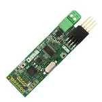
The circuit shown in Figure 1 is built on the DEMO-AD5700D2Z
printed circuit board shown in Figure 3.
The DEMO-AD5700D2Z circuit board includes some additional
features for easy system evaluation. The 0.1 inch-pitch connector
footprints allow optional primary and secondary sensor
connections. There are test points for HART RTS and CD
that may be needed for HART compliance tests.
DN2540
BSP129
200kΩ
Circuit Hardware
Figure 3. DEMO-AD5700D2Z Printed Circuit Board (Pressure Sensor Not Included)
AD5421
REGIN
CIRCUIT EVALUATION AND TEST
10551-003
The ADuCM361 on-chip DAC with an external transistor can
be used to control the 4 mA to 20 mA loop, refer to CN-0300
for details.
Figure 2. MOSEFT Connected to the AD5421 Loop Power Supply
The AD5700 is used with a 3.8664 MHz crystal in this circuit,
which is the configuration achieving the lowest power consumption.
Alternatively, the AD5700-1, with an integrated 0.5 %precision
internal oscillator, can be used. The internal oscillator increases
the modem power supply current by 225 µA maximum, compared
to the crystal oscillator, but because no external crystal is needed,
this option provides both cost savings and reduced board area
requirements.
For the applications that are not loop powered, the AD5410,
AD5420, AD5422, or AD5755 are good choices for the 4 mA to
20 mA DAC.
A connector on the edge of the DEMO-AD5700D2Z makes the
ADuCM360 single wire and UART download/debug signals
accessible allowing easy software development, code download,
and in-circuit debugging and emulation. The connector, with a
small header extender included with the DEMO-AD5700D2Z
board, is compatible with all Analog Devices, Inc., Cortex-M3
based development tools, such as the EVAL-ADuCM360QSPZ
evaluation kit (the evaluation kit is not included with the
DEMO-AD5700D2Z board).
These features are not shown in the simplified diagram in Figure 1;
however, they can be seen in the complete circuit schematic in
the CN-0267 Design Support Package. The design support package
also includes a full field instrument C-code example, which
enables complete verification and evaluation of all hardware
blocks and features of the circuit, and a limited verification of
the HART interface functionality. For detailed information about
HART interface specifications and resources, contact the Hart
Communication Foundation.
HART Compliance
The DEMO-AD5700D2Z has been verified to be compliant with
HART FSK Physical Layer Specification (HCF_SPEC-054,
Revision 8.1), using methods and equipment specified in the
HART Physical Layer Test Specification (HCF_TEST-2,
Revision 2.2). The board was submitted to the Hart
Communication Foundation and was successfully registered.
The registered circuit can be found on the HART Communication
Foundation (HFC) web site in the product catalog as DEMOAD5700D2Z.
The results of two of the tests involved the output noise during
silence and the analog rate of change.
Rev. B | Page 4 of 8
�Circuit Note
CN-0267
When a HART device is not transmitting (silence), do not couple
noise onto the network. Excessive noise may interfere with
reception of HART signals by the device itself or other devices
on the network.
The voltage noise measured across a 500 Ω load in the loop must
contain no more than 2.2 mV rms of combined broadband and
correlated noise in the HART extended frequency band. In
addition, the noise should not exceed 138 mV rms outside the
HART extended frequency band.
This noise was measured by a true rms meter across the 500 Ω
load. This noise was measured directly for the out-of-band noise
and measured through the HCF_TOOL-31 filter for the in-band
noise. An oscilloscope was also used to examine the noise
waveform.
The noise was measured at the worse condition, which was 4 mA
output current. The captured noise waveform is shown in
Figure 4, and the results are summarized in Table 1.
The hardware slew-rate limit is set by the capacitance connected
to the AD5421 CIN pin. When a large step change is required in
the analog output current value, the ADuCM360 software splits
the output current change sent to the AD5421 DAC into a number
of smaller subsequent steps.
This test was performed using an oscilloscope coupled to the
500 Ω load through the HCF_TOOL-31 filter.
The result is shown in Figure 5. Waveform CH1 shows the periodic
steps between 4 mA and 20 mA, sensed directly across the 500 Ω
load. Waveform CH2 is the signal captured on the HCF_TOOL-31
filter output, amplified 10×, within the 150 mV peak limits.
CH1
FREQ
8.123Hz?
1
CH2
OUTPUT OF
FILTER × 10
MEASURE
CH1
p-p
44.8mV
CH2
p-p
254mV
2
CH2
MAX
134mV
LIMIT =
±150mV
CH1
CYC RMS
4.64mV?
CH2
MIN
–120mV
CH1
NONE
1
MEASURE
CH1
p-p
8.60V
CH1
4mA TO 20mA
ACROSS 500Ω
CH1 5.00V
CH2 50mV BW
M 25.0ms
CH1
6.80V
10551-005
Output Noise During Silence Test
Figure 5. Analog Rate of Change Waveform
Circuit Power Consumption
CH1
NONE
Two methods were used to evaluate the circuit power consumption
performance.
M 100ms
CH1
–8.00mV