EV-ADF4159EB1Z/EV-ADF4159EB3Z User Guide
UG-383
One Technology Way • P.O. Box 9106 • Norwood, MA 02062-9106, U.S.A. • Tel: 781.329.4700 • Fax: 781.461.3113 • www.analog.com
Evaluating the ADF4159 Frequency Synthesizer for Phase-Locked Loops
FEATURES
REQUIRED SOFTWARE
Self-contained board, including synthesizer, 100 MHz
reference, USB interface, and voltage regulators
Accompanying software allows control of synthesizer
functions from a PC (via USB interface)
Externally powered by 5.5 V and 15 V supplies
Analog Devices ADF4158-9 evaluation software, Version 4.x
or higher (included on the CD in the evaluation board kit or
available for download at www.analog.com)
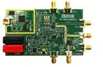
GENERAL DESCRIPTION
The EV-ADF4159EB1Z/ EV-ADF4159EB3Z evaluates the
performance of the ADF4159 frequency synthesizer for phaselocked loops (PLL). A photograph of the evaluation board is
shown in Figure 1. The evaluation board involves the ADF4159
synthesizer, a USB connector, SMA connectors, a reference
oscillator, and power supply connectors. There are also footprints
for active filter components and a voltage controlled oscillator
(VCO); if used, these components must be soldered to the board
to complete the loop. An on-board temperature compensated
crystal oscillator (TCXO) provides the 100 MHz reference
frequency, and a USB cable is included to connect the board to
a PC USB port.
EVALUATION KIT CONTENTS
EV-ADF4159EB1Z or EV-ADF4159EB3Z evaluation board
CD with evaluation software
USB cable
REQUIRED ADDITIONAL EQUIPMENT
VCO (for EV-ADF4159EB3Z)
Loop filter components (for EV-ADF4159EB3Z)
Soldering equipment
Spectrum analyzer
Power supplies (5.5 V and 15 V)
Windows®-based PC with USB port for evaluation software
In addition, the evaluation kit contains Windows-based software
to allow easy programming of the synthesizer.
REQUIRED DOCUMENTS
ADF4159 data sheet
UG-383 user guide
10572-001
EVALUATION BOARD PHOTOGRAPH
Figure 1.
PLEASE SEE THE LAST PAGE FOR AN IMPORTANT
WARNING AND LEGAL TERMS AND CONDITIONS.
Rev. B | Page 1 of 16
�UG-383
EV-ADF4159EB1Z/EV-ADF4159EB3Z User Guide
TABLE OF CONTENTS
Features .............................................................................................. 1
Output Signals ...............................................................................3
Evaluation Kit Contents ................................................................... 1
Loop Filter ......................................................................................4
Required Additional Equipment .................................................... 1
VCO Configuration ..........................................................................5
Required Documents ....................................................................... 1
EV-ADF4159EB1Z........................................................................5
Required Software ............................................................................ 1
EV-ADF4159EB3Z........................................................................5
General Description ......................................................................... 1
Evaluation Setup ................................................................................6
Evaluation Board Photograph......................................................... 1
Getting Started ...................................................................................7
Revision History ............................................................................... 2
Installing the Software ..................................................................7
Evaluation Board Hardware ............................................................ 3
Configuring and Setting up the Board .......................................7
Overview........................................................................................ 3
Using the Software—Main Controls...........................................8
Power Supplies .............................................................................. 3
Using the Software—Ramp and Shift-Key Controls ................9
Local Oscillator ............................................................................. 3
Evaluation Board Schematics........................................................ 11
VCO................................................................................................ 3
REVISION HISTORY
7/14—Rev. A to Rev. B
Changes to Sample Loop Filter Section ......................................... 4
11/13—Rev. 0 to Rev. A
Deleted EV-ADF4159EB2Z .............................................. Universal
Changes to Figure 7 .......................................................................... 8
Changes to Figure 8 .......................................................................... 9
Changes to Figure 9 ........................................................................ 10
8/13—Revision 0: Initial Version
Rev. B | Page 2 of 16
�EV-ADF4159EB1Z/EV-ADF4159EB3Z User Guide
UG-383
EVALUATION BOARD HARDWARE
OVERVIEW
LOCAL OSCILLATOR
The evaluation board kit includes a cable for connecting the
evaluation board to the USB port of a PC. The silkscreen for the
evaluation board is show in Figure 2, and the schematics for the
evaluation board are shown in Figure 10 to Figure 13.
The 100 MHz TXCO provides the reference frequency. To
ensure that the PFD frequency is also 100 MHz, set the on-chip
R-divider to 1.
POWER SUPPLIES
Alternatively, an external reference can be used by connecting
the reference to the REFIN SMA and removing R10 and L1.
The evaluation board is powered by a 5.5 V power supply connected to the red and black banana connectors. Connect the
red connector to a 5.5 V power supply and the black connector
to ground.
VCO
The op amp is powered by a 15 V power supply.
OUTPUT SIGNALS
Optionally, the VCO can be powered independently by connecting
a 5 V supply to the VVCO SMA and removing R27. When this
option is used, reduce the voltage on the banana connectors to 5 V.
With a VCO connected, the evaluation board outputs the VCO
output on the EXT_VCOOUT SMA and the VCO output is
divided by 2 on the VCO/2 SMA.
The VCO configuration is different for each evaluation board
model: EV-ADF4159EB1Z and EV-ADF4159EB3Z. See the
VCO Configuration section for more information.
10572-002
The USB section of the evaluation board (see the area bounded
by the gold box in Figure 1) is powered by the USB host.
Figure 2. Evaluation Board Silkscreen
Rev. B | Page 3 of 16
�UG-383
EV-ADF4159EB1Z/EV-ADF4159EB3Z User Guide
LOOP FILTER
Sample Loop Filter
The loop filter schematic is included in Figure 13. The general
placement of loop filter components is shown in Figure 3. When
using a loop filter, calculate the values of the necessary components and solder them to the board. The ADIsimPLL software,
which is available on the CD included in the evaluation board kit or
from www.analog.com/adisimpll, provides tools for designing loop
filters and calculating component values.
Use the parameters of the sample loop filter described in this
section as a guide for adding a loop filter onto the evaluation
board.
After soldering the loop filter components to the evaluation board,
connect a 15 V supply to the op amp power supplies, a 15 V supply
to the red 15 V test point, and the ground to the black AGND
test point (see Figure 1). See the Sample Loop Filter section for
an example configuration.
The sample loop filter is designed for
•
•
•
•
•
VCO kV = 150 MHz/V
PFD frequency = 100 MHz
Charge pump current = 2.5 mA
Loop bandwidth = 282 kHz
Phase margin = 48.1°
Table 1. Sample Loop Filter Components Values
C1
Component
R1
C1
R2
C2
R3
C3
C4
R1
R2
C3
Refer to Figure 3 for proper placement of components and to
Table 1 for recommended component values.
OP AMP
C2
C4
10572-003
R3
Figure 3. Placement of Loop Filter Components
Rev. B | Page 4 of 16
Value
100 Ω
220 pF
360 Ω
5.6 nF
1 kΩ
180 pF
180 pF
�EV-ADF4159EB1Z/EV-ADF4159EB3Z User Guide
UG-383
VCO CONFIGURATION
EV-ADF4159EB1Z
EV-ADF4159EB3Z
The EV-ADF4159EB1Z evaluation board has a MACOM VCO
(MAOC-009269) with a range of 11.4 GHz to 12.8 GHz installed.
The RFOUT signal is connected to the EXT_VCOOUT SMA.
The RFOUT/2 signal of the VCO is fed back to the ADF4159
PLL; therefore, when the VCO outputs 12 GHz, the ADF4159 is
locked at 6 GHz.
The EV-ADF4159EB3Z evaluation board does not have a VCO
installed. The board is configured for use with an external VCO
board. Connect an external VCO to the evaluation board using
SMA cables. There are two configuration options:
For optimum performance, ensure that the components values
are as described in Table 2.
•
•
Table 2. Component Values for EV-ADF4159EB1Z
Component
R73
C29
R31, R34, R51, R62, R68, R70,
R71, R72 (Bottom Layer)
C40, C62, C63, C64, C65, C66,
C70, C71, C75, C76
L3, L4
1
Value1
0Ω
100 pF
DNP
DNP
DNP
DNP is do not populate.
Terminate the VCO/2 SMA with 50 Ω..
The VCO control voltage can be connected to the VTUNE
SMA, and the VCO RFOUT signal can be connected to the
VCO/2 SMA. This configuration uses the on-board loop filter.
The CPOUT SMA can be used to connect the ADF4159
charge pump output to an external loop filter. Connect the
VCO RFOUT signal to the VCO/2 SMA to feed the signal
back into the ADF4159.
For optimum performance, ensure that the component values
are as shown in Table 3.
Table 3. Component Values for EV-ADF4159EB3Z
Component
R34
R31
C29
1
DNP is do not populate.
Rev. B | Page 5 of 16
Value1
50 Ω
DNP
DNP
�UG-383
EV-ADF4159EB1Z/EV-ADF4159EB3Z User Guide
EVALUATION SETUP
REFERENCE
CRYSTAL
TO PC
GND
ADF4159
15V
50Ω TERMINATION
VCO
TO SPECTRUM ANALYZER
Figure 4. Evaluation Setup Block Diagram
10572-005
5.5V
OP AMP
10572-004
GND
Figure 5. Evaluation Setup
Rev. B | Page 6 of 16
�EV-ADF4159EB1Z/EV-ADF4159EB3Z User Guide
UG-383
GETTING STARTED
INSTALLING THE SOFTWARE
4.
For the software installation procedure, see the UG-476 user
guide. The control software for the EV-ADF4159EB1Z and EVADF4159EB3Z is provided on the CD included in the evaluation
board kit.
5.
CONFIGURING AND SETTING UP THE BOARD
Set up the circuit as shown in Figure 4.
Run the ADF4158-9 software.
Select ADF4159 and USB board (green), and then click
Connect (see Figure 6).
6.
10572-007
1.
2.
3.
Click the Main Controls tab to view the main controls (see
Figure 7). The default values are set to lock a VCO at 12 GHz.
Click Write All Registers (7, 6, 6, 5, 5, 4, 4, 3, 2, 1, 0) or
manually write to each register (Write R7, Write R6 - Ramp 1,
Write R6 - Ramp 2, Write R5 - Ramp 1, Write R5 - Ramp 2,
Write R4 - Ramp 1, Write R4 - Ramp 2, Write R3, Write R2,
Write R1, and Write R0).
On the spectrum analyzer, confirm that the output signal is
locked at 12 GHz.
Figure 6. Software—Device Selection
Rev. B | Page 7 of 16
�UG-383
EV-ADF4159EB1Z/EV-ADF4159EB3Z User Guide
USING THE SOFTWARE—MAIN CONTROLS
Use the Main Controls tab to select the RL and PLL settings.
Because the evaluation board is set up to feedback the VCO/2
output to the ADF4159, in the RF Settings area, set the RF VCO
Output Frequency to half the VCO output. Set the Reference
Frequency to be the same as the applied reference signal. The
PFD frequency is calculated from the reference frequency, the
R-counter, the reference doubler, and the reference-divide-by-2.
Ensure that the value in the PFD Frequency box matches the
value specified in the loop filter design.
The Muxout drop-down box allows you to choose the signal
that is connected to the output of the MUXOUT pin.
Clicking Pulse TXdata triggers a pulse on the TXDATA pin. This
pulse starts low and then stays high for approximately 4 µs.
The register values are shown at the bottom of the window.
When the background of a register value is green, this indicates
that the value has been changed and needs to be written to the
part. Clicking the button below each register value writes that
value to the part.
10572-008
In the PLL Settings area, program the Charge Pump Setting
to the value for which the loop filter was designed. Program the
Phase Detector Polarity to negative when using an inverting
active loop filter configuration (as is on this evaluation board).
Figure 7. Software—Main Controls
Rev. B | Page 8 of 16
�EV-ADF4159EB1Z/EV-ADF4159EB3Z User Guide
USING THE SOFTWARE—RAMP AND SHIFT-KEY
CONTROLS
In the Ramps and Shift-keying tab, you can configure the
ramping and shift-keying functionality of the ADF4159.
The ramp type can be selected in the Ramp mode drop-down
box, and the various ramp parameters can be set in CLK1 and
Up Ramp boxes.
Example
UG-383
over 50 MHz with an up ramp time of 96 µs. (Up ramp refers to
the ramp from the initial frequency to the end frequency,
whereas down ramp refers to the ramp/jump from the end
frequency back to the initial frequency.) For 50 MHz, the PLL is
programmed for a 25 MHz ramp because the evaluation board
uses the RFOUT/2 signal. After each parameter is set in the
software, it needs to be written to the part.
The other options in this tab allow configuring the various
ramps and shift-keying controls of the ADF4159.
10572-006
Figure 8 shows the ramping and shift-keying settings for an
example of a continuous triangular ramp of 128 up ramp steps
Figure 8. Example of Ramp
Rev. B | Page 9 of 16
�EV-ADF4159EB1Z/EV-ADF4159EB3Z User Guide
10572-009
UG-383
Figure 9. Software—Ramp Controls
Rev. B | Page 10 of 16
�Rev. B | Page 11 of 16
Figure 10. Evaluation Board Schematic (Page 1)
LE
DATA
CLK
L1
470Ω AT 100MHz
R61
10pF
R59
DNP
330Ω
330Ω
R19
R9
AGND
330Ω
R18
AGND
AGND AGND
R64
10kΩ
Y3
GND
2
AGND
AGND
R17
390Ω
R13
390Ω
CLK DATA LE
AGND
Y1
COMP 5
GND
3
100.0MHz
RF_OUT 4
TX-500
R15
390Ω
1 VC
6 VS
RF-OUT 5
GND
3
1 TRI
AGND
RF_OUT 4
6 VS
VFXO321-BBEC-100MHz
1 E/D
REFIN
T1
CE
C11
R53
330Ω
AGND
TXDATA
TXD
R10
91Ω
DNP
R11
1nF
CE
10pF
1nF
390Ω
R65
AGND
DNP
R12
C12
AGND
R14
R7
10kΩ
+1.8V
0.1µF
C20
C18
R5
0Ω
+3V
AGND
AGND
12 TXDATA
16 LE
15 DATA
14 CLK
9 REFIN
13 CE
AGND
10pF
0.1µF
C10
C9
R63
0Ω
+1.8V
U1
ADF4159
VP
17
5
23
20
24
RFINB 4
MUXOUT
RFINA
RSET
SW2
CP
21
22
10pF
C19
C16
C7
AGND
C42
100pF
5.1kΩ
R4
TSW2
10pF
0.1µF
AGND
TSW1
VP
0.1µF
C21
R48
0Ω
+1.8V
SW3
8
AVDD
4 VCC RF_OUT 3
7
AVDD
10 DGND
OSC_VDD
22µF
C35
6
AVDD
11 SDGND
3 AGND
C34
19
DVDD
Y4
TXDATA
18
SDVDD
2 AGND
1 CPGND
XTAL-CWX113-100MHz
1kΩ
R28
RFIN
AGND
CPOUT
MUXOUT
R6
0Ω
CPOUT
D1
LOCK DETECT
MUXOUT
EV-ADF4159EB1Z/EV-ADF4159EB3Z User Guide
UG-383
EVALUATION BOARD SCHEMATICS
10572-010
�Rev. B | Page 12 of 16
Figure 11. Evaluation Board Schematic (Page 2)
GND
BANANA-BLACK
D2
1N4001
BANANA-RED
VSUPPLY
0Ω
R52
R22
DNP
R21
0Ω
AGND
AGND1
C15
1µF
DNP
R54
C13
1µF
+15V
5
8
R29
DNP
0Ω
R25
EN
VIN
U8
1µF
C31
7
2
4
10Ω
R20
GND EP GND
3
6
9
PG
ADJ
N/C
VOUT
EN/UVLO
VIN
1
GND
2
U13
5
+15V
VOUT
ADP150-TSOT-3.3V
ADP7104ARZ
3
1
0Ω
R46
R30
DNP
C41
1µF
0Ω
R55
C17
10µF
C43
DNP
R67
DNP
4.7µH
L2
OSC_VDD
+
+5V
+ C6
100µF
R24
0.33Ω
+5V1
R47
DNP
5V_USB
C32
1µF
C5
1µF
C8
1µF
R33
DNP
0Ω
R32
R36
DNP
0Ω
R35
R42
DNP
0Ω
R37
3
1
3
1
3
1
VOUT
GND
2
U2
5
VOUT
GND
2
U3
5
EN
VIN
GND
2
U10
VOUT
5
ADP150-TSOT-3.0V
EN
VIN
ADP150-TSOT-1.8V
EN
VIN
ADP150-TSOT-3.0V
C33
1µF
0Ω
R57
C30
1µF
0Ω
R60
C28
1µF
0Ω
R56
VP
+1.8V
+3V
VP
+1.8V
D3
R38
1kΩ
+3V
UG-383
EV-ADF4159EB1Z/EV-ADF4159EB3Z User Guide
10572-011
�AGND
6
7
8
9
0Ω
R58
DGND
USB
USB-MINI-B
1
VBUS
2
D–
SHLD1
3
SHLD2
D+
SHLD3
4
SHLD4
IO
5
GND
D4
R39
2.2kΩ
5V_USB
+
TRIG
OUT
OUT
FB
NC
1
2
3
4
C55
0.1µF
C54
0.1µF
CE
TXDATA
DATA
CLK
LE
R45
100kΩ
R44
100kΩ
3.3V-USB
78.7kΩ
ADP3334
R41
3.3V-USB
C48
22µF
IN
IN
SD
GND
C53
C52
1nF
C49
0.1µF
C44
0.1µF
C45
0.1µF
C46
0.1µF
C58
0.1µF
C59
0.1µF
C60
0.1µF
10pF
3.3V-USB
140kΩ
R40
PA0/INT0
PA1/INT1
PA2/*SLOE
PA3/*WU2
PA4/FIFOADR0
PA5/FIFOADR1
PA6/*PKTEND
PA7/*FLD/SLCS
1
2 RDY0/*SLRD
RDY1/*SLWR
13
IFCLK
14 RSVD
33
34
35
36
37
38
39
40
0.1µF
C61
C50
+
XTALIN
XTALOUT
5
4
16
SDA
SCL 15
29
CTL0/*FLAGA 30
CTL1/*FLAGB
CTL2/*FLAGC 31
18
19
20
21
22
23
24
25
45
46
47
48
49
50
51
52
C51
22µF
3.3V-USB
PB0/FD0
PB1/FD1
PB2/FD2
PB3/FD3
PB4/FD4
PB5/FD5
PB6/FD6
PB7/FD7
PD0/FD8
PD1/FD9
PD2/FD10
PD3/FD11
PD4/FD12
PD5/FD13
PD6/FD14
PD7/FD15
3.3V-USB
1µF
U6
CY7C68013-CSP
CLKOUT
9
8 DD+
54
42
RESET
44 *WAKEUP
DECOUPLING FOR U7 - PLACE ONE CLOSE TO EACH VCC PIN
3.3V-USB
1µF
C47
8
7
6
5
U5
3
AVCC
3.3V_USB
VCC
VCC
VCC
VCC
VCC
VCC
VCC
7
11
17
27
32
43
55
AGND
6
Rev. B | Page 13 of 16
GND
GND
GND
GND
GND
GND
GND
Figure 12. Evaluation Board Schematic (Page 3)
10
12
26
28
41
53
56
5V_USB
C26
12pF
C57
24.0MHz
Y2
8
VCC 7
WP 6
SCL 5
SDA
10pF
0.1µF
U7
C27
12pF
R49
2.2kΩ
MUXOUT
3.3V-USB
C56
24LC64
1
2 A0
3 A1
4 A2
VSS
3.3V-USB
0R
R43
SCREEN BOX
R50
2.2kΩ
3.3V-USB
EV-ADF4159EB1Z/EV-ADF4159EB3Z User Guide
UG-383
10572-012
�EV-ADF4159EB1Z/EV-ADF4159EB3Z User Guide
10572-013
UG-383
Figure 13. Evaluation Board Schematic (Page 4)
Rev. B | Page 14 of 16
�EV-ADF4159EB1Z/EV-ADF4159EB3Z User Guide
NOTES
Rev. B | Page 15 of 16
UG-383
�UG-383
EV-ADF4159EB1Z/EV-ADF4159EB3Z User Guide
NOTES
ESD Caution
ESD (electrostatic discharge) sensitive device. Charged devices and circuit boards can discharge without detection. Although this product features patented or proprietary protection
circuitry, damage may occur on devices subjected to high energy ESD. Therefore, proper ESD precautions should be taken to avoid performance degradation or loss of functionality.
Legal Terms and Conditions
By using the evaluation board discussed herein (together with any tools, components documentation or support materials, the “Evaluation Board”), you are agreeing to be bound by the terms and conditions
set forth below (“Agreement”) unless you have purchased the Evaluation Board, in which case the Analog Devices Standard Terms and Conditions of Sale shall govern. Do not use the Evaluation Board until you
have read and agreed to the Agreement. Your use of the Evaluation Board shall signify your acceptance of the Agreement. This Agreement is made by and between you (“Customer”) and Analog Devices, Inc.
(“ADI”), with its principal place of business at One Technology Way, Norwood, MA 02062, USA. Subject to the terms and conditions of the Agreement, ADI hereby grants to Customer a free, limited, personal,
temporary, non-exclusive, non-sublicensable, non-transferable license to use the Evaluation Board FOR EVALUATION PURPOSES ONLY. Customer understands and agrees that the Evaluation Board is provided
for the sole and exclusive purpose referenced above, and agrees not to use the Evaluation Board for any other purpose. Furthermore, the license granted is expressly made subject to the following additional
limitations: Customer shall not (i) rent, lease, display, sell, transfer, assign, sublicense, or distribute the Evaluation Board; and (ii) permit any Third Party to access the Evaluation Board. As used herein, the term
“Third Party” includes any entity other than ADI, Customer, their employees, affiliates and in-house consultants. The Evaluation Board is NOT sold to Customer; all rights not expressly granted herein, including
ownership of the Evaluation Board, are reserved by ADI. CONFIDENTIALITY. This Agreement and the Evaluation Board shall all be considered the confidential and proprietary information of ADI. Customer may
not disclose or transfer any portion of the Evaluation Board to any other party for any reason. Upon discontinuation of use of the Evaluation Board or termination of this Agreement, Customer agrees to
promptly return the Evaluation Board to ADI. ADDITIONAL RESTRICTIONS. Customer may not disassemble, decompile or reverse engineer chips on the Evaluation Board. Customer shall inform ADI of any
occurred damages or any modifications or alterations it makes to the Evaluation Board, including but not limited to soldering or any other activity that affects the material content of the Evaluation Board.
Modifications to the Evaluation Board must comply with applicable law, including but not limited to the RoHS Directive. TERMINATION. ADI may terminate this Agreement at any time upon giving written notice
to Customer. Customer agrees to return to ADI the Evaluation Board at that time. LIMITATION OF LIABILITY. THE EVALUATION BOARD PROVIDED HEREUNDER IS PROVIDED “AS IS” AND ADI MAKES NO
WARRANTIES OR REPRESENTATIONS OF ANY KIND WITH RESPECT TO IT. ADI SPECIFICALLY DISCLAIMS ANY REPRESENTATIONS, ENDORSEMENTS, GUARANTEES, OR WARRANTIES, EXPRESS OR IMPLIED, RELATED
TO THE EVALUATION BOARD INCLUDING, BUT NOT LIMITED TO, THE IMPLIED WARRANTY OF MERCHANTABILITY, TITLE, FITNESS FOR A PARTICULAR PURPOSE OR NONINFRINGEMENT OF INTELLECTUAL
PROPERTY RIGHTS. IN NO EVENT WILL ADI AND ITS LICENSORS BE LIABLE FOR ANY INCIDENTAL, SPECIAL, INDIRECT, OR CONSEQUENTIAL DAMAGES RESULTING FROM CUSTOMER’S POSSESSION OR USE OF
THE EVALUATION BOARD, INCLUDING BUT NOT LIMITED TO LOST PROFITS, DELAY COSTS, LABOR COSTS OR LOSS OF GOODWILL. ADI’S TOTAL LIABILITY FROM ANY AND ALL CAUSES SHALL BE LIMITED TO THE
AMOUNT OF ONE HUNDRED US DOLLARS ($100.00). EXPORT. Customer agrees that it will not directly or indirectly export the Evaluation Board to another country, and that it will comply with all applicable
United States federal laws and regulations relating to exports. GOVERNING LAW. This Agreement shall be governed by and construed in accordance with the substantive laws of the Commonwealth of
Massachusetts (excluding conflict of law rules). Any legal action regarding this Agreement will be heard in the state or federal courts having jurisdiction in Suffolk County, Massachusetts, and Customer hereby
submits to the personal jurisdiction and venue of such courts. The United Nations Convention on Contracts for the International Sale of Goods shall not apply to this Agreement and is expressly disclaimed.
©2013–2014 Analog Devices, Inc. All rights reserved. Trademarks and
registered trademarks are the property of their respective owners.
UG10572-0-7/14(B)
Rev. B | Page 16 of 16
�