ADF7030-1 Hardware Reference Manual
UG-957
One Technology Way • P.O. Box 9106 • Norwood, MA 02062-9106, U.S.A. • Tel: 781.329.4700 • Fax: 781.461.3113 • www.analog.com
ADF7030-1 Hardware Reference Manual
SCOPE
The ADF7030-1 features an on-chip ARM® Cortex®-M0
processor that performs radio control and radio packet
management.
This reference manual provides a description of the ADF7030-1
radio functionality, hardware features, and application circuit
requirements. It is intended as a resource for a hardware engineer
designing a printed circuit board (PCB) that includes the
ADF7030-1.
OTHER RELEVANT DOCUMENTATION
Complete specifications for the ADF7030-1 device can be found
in the ADF7030-1 data sheet. The ADF7030-1 software reference
manual is the programming guide for the ADF7030-1 and is
available from Analog Devices, Inc. Both the ADF7030-1 data
sheet and software reference manual documents should be
consulted in conjunction with this hardware reference manual.
ABOUT THE ADF7030-1
The ADF7030-1 is a low power, high performance, fully
integrated radio transceiver that supports a wide range of
modulation scheme and channel widths in the sub GHz
frequency range.
CREGx
HFXTALN HFXTALP
GPIO6 GPIO7
ADF7030-1
LDOx
LNAIN1
LNAIN2
TCXO
BUFFER
LNA
26MHz
OSC
32kHz
OSC
26kHz
RCOSC
INTERRUPT
CONTROLLER
ARM®
CORTEX®-M0
RECEIVER
DIGITAL
BASEBAND
PAOUT1
PA
SPI
SLAVE
CONFIGURABLE
GPIOs
SYNTHESIZER
SPI
GPIOx
ROM
PA
TRANSMITTER
RAM
NOTES
1. CREGx, GPIOx, AND SPI CONTAIN MULTIPLE PINS.
Figure 1. Functional Block Diagram
PLEASE SEE THE LAST PAGE FOR AN IMPORTANT
WARNING AND LEGAL TERMS AND CONDITIONS.
TEMP SENSOR
14383-001
PAOUT2
Rev. B | Page 1 of 16
�UG-957
ADF7030-1 Hardware Reference Manual
TABLE OF CONTENTS
Scope .................................................................................................. 1
PA2 Separate Matching Network ............................................. 11
About the ADF7030-1...................................................................... 1
LNA Separate Matching Network ............................................ 12
Other Relevant Documentation ..................................................... 1
Combined Matching Network .................................................. 12
Revision History ............................................................................... 2
Bill of Materials Count ................................................................... 14
Getting Started .................................................................................. 3
Reference Design ........................................................................ 14
Evaluation and Development Platform ..................................... 3
Layout and Stack Up .................................................................. 15
ADF7030-1 Pin Descriptions .......................................................... 4
Test Mode Connections ................................................................. 16
Pin Functions ................................................................................ 4
Transmit Test Mode Connections ............................................ 16
Frequency References .................................................................. 5
Receive Test Mode Connections .............................................. 16
Application Circuit Diagrams ......................................................... 7
Related Links ............................................................................... 16
RF Matching Networks .................................................................. 10
PA1 Separate Matching Network ............................................. 10
REVISION HISTORY
7/2020—Rev. A to Rev. B
Changes to Table 2 ............................................................................ 3
Changes to Table 3 ............................................................................ 4
Changes to Application Circuit Diagrams Section ...................... 7
Added Figure 7; Renumbered Sequentially .................................. 9
Changes to Table 6 and Table 7 ..................................................... 10
Changes to Table 8 and Table 9 ..................................................... 11
Changes to Table 10 and Table 11 ................................................ 12
Added Combined Matching Network Section, Figure 12, and
Table 12; Renumbered Sequentially ............................................. 12
9/2017—Rev. 0 to Rev. A
Changes to Crystal Reference Section ............................................5
Changes to Application Circuit Diagrams Section .......................7
Changes to PA1 Separate Matching Network Section, Figure 7,
Figure 8, and Figure 9 .................................................................... 10
Changes to Table 10 and Table 11 ................................................ 13
6/2016—Revision 0: Initial Version
Rev. B | Page 2 of 16
�ADF7030-1 Hardware Reference Manual
UG-957
GETTING STARTED
EVALUATION AND DEVELOPMENT PLATFORM
Table 1. ADF7030-1 EZ-KIT Kit Models
The ADF7030-1 EZ-KIT is an evaluation and development
systems for the ADF7030-1 high performance, sub GHz radio
transceiver IC.
The ADF7030-1 EZ-KIT allows fast and thorough evaluation of
the ADF7030-1 and provides a platform for host processor code
development.
There are four models of the ADF7030-1 EZ-KIT available as
described in Table 1, each covering one of the main industrial,
scientific and medical (ISM) bands at 169 MHz, 433 MHz,
868 MHz, or 915 MHz.
Model
ADF70301-915EZKIT
ADF70301-868EZKIT
ADF70301-433EZKIT
ADF70301-169EZKIT
Frequency (MHz)
902 to 928
863 to 876
433 to 434
169
The ADF7030-1 EZ-KIT kit models in Table 1 include RF
daughter boards. Additional daughter boards covering different
frequency ranges (for example, 450 MHz to 470 MHz) or with
different matching topologies can be ordered individually and
used with the ADF7030-1 EZ-KIT as described in Table 2.
Table 2. ADF7030-1 Daughter Boards
Board Name
EV-ADF70301-915AZ
EV-ADF70301-915CZ
EV-ADF70301-915DZ
EV-ADF70301-915EZ
EV-ADF70301-868BZ
EV-ADF70301-868EZ
EV-ADF70301-460BZ
EV-ADF70301-433AZ
EV-ADF70301-433CZ
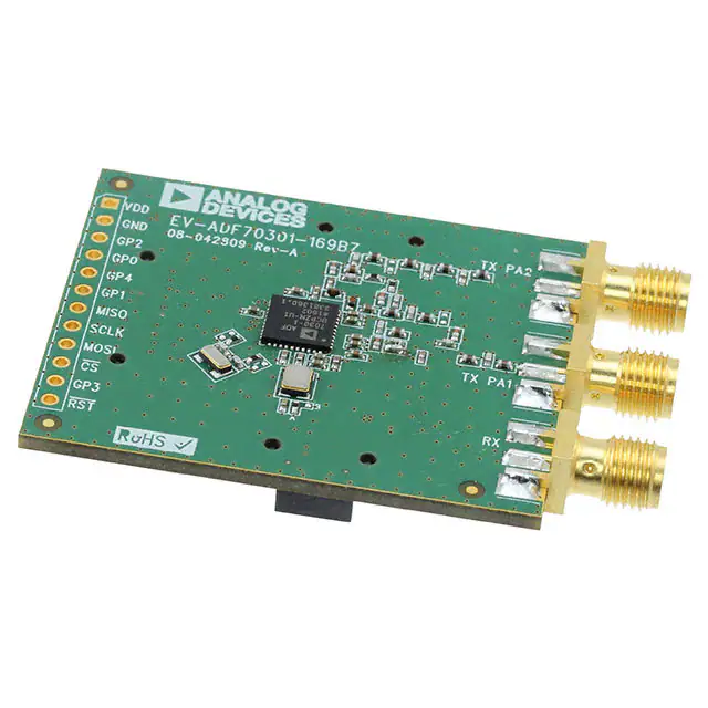
EV-ADF70301-169BZ
Match
Separate
Combined
Combined
Combined
Separate
Combined
Separate
Separate
Combined
Separate
Frequency (MHz)
915
915
915
915
868
868
460
433
433
169
Reference Populated
XTAL
XTAL
TCXO
XTAL
TCXO
XTAL
TCXO
XTAL
XTAL
TCXO
Rev. B | Page 3 of 16
Reference Connected
XTAL
XTAL
TCXO
XTAL
TCXO
XTAL
TCXO
XTAL
XTAL
TCXO
PA Connected
Both
PA1
PA1
PA2
Both
PA2
Both
Both
PA1
Both
�UG-957
ADF7030-1 Hardware Reference Manual
ADF7030-1 PIN DESCRIPTIONS
PIN FUNCTIONS
As a result, the minimum supply voltage requirement increases
with increased transmit power, as detailed in Table 4. Output
powers in excess of 13 dBm apply to only Power Amplifier 2 (PA2).
For all pins, do not exceed the absolute maximum ratings
specified in the ADF7030-1 data sheet.
Hardware Reset Pin
When the hardware reset pin (RST) is pulled low by a host
microprocessor, the ADF7030-1 undergoes a hardware reset.
Timing requirements for this pull-down duration are given in
the ADF7030-1 data sheet.
To prevent unintended resets, a 100 kΩ pull-up resistor is
recommended on the RST pin. Refer to the digital input/output
specifications in the ADF7030-1 data sheet for information on
logic level requirements.
SPI Interface
The serial peripheral interface (SPI) of the ADF7030-1 consists
of the CS, SCLK, MISO, and MOSI pins. The ADF7030-1 acts as
an SPI slave to an external host microprocessor. If the device is
in the PHY_SLEEP state, pulling the CS pin to change low wakes
the ADF7030-1. To prevent unintentional wake up of the
ADF7030-1, a 100 kΩ pull-up resistor is recommended on
the CS pin.
Refer to the digital input/output specifications in the ADF7030-1
data sheet for information on logic level and timing requirements.
Regulator Stability Capacitors
A 220 nF capacitor connected to ground is required at each of the
CREG1, CREG2, CREG3, CREG4, CREG5, CREG6, and CREG7
pins of the ADF7030-1. Place each 220 nF capacitor as close to
the pin as possible to ensure regulator stability and noise rejection.
In addition to the 220 nF capacitor, a second capacitor to ground is
recommended at the CREG3 pin. The second capacitor reduces
the amplitude of the power amplifier (PA) harmonics transmitted
to the device. Place this second decoupling capacitor between
the 220 nF regulator capacitor and the CREG3 pin, as close to
the pin as possible. Recommended values for this second
decoupling capacitor are listed in Table 3.
Table 3. Recommended Capacitor Values at the CREG3 Pin
for Harmonic Suppression
Frequency (MHz)
915
868
460
433
169
Value (pF)
6.8
18
47
68
220
The ADF7030-1 software reference manual describes selecting
the desired PA, programming the PA output level, and setting
the CREG3 voltage.
Table 4. Required Supply Voltage vs. Transmit Power Level
Tx Power
Level (dBm)
≥17
16
15
14
13
很抱歉,暂时无法提供与“EV-ADF70301-169BZ”相匹配的价格&库存,您可以联系我们找货
免费人工找货