GaAs, SPDT Switch, Nonreflective,
100 MHz to 12 GHz
HMC232A
Data Sheet
NIC 1
19 NIC
20 NIC
21 GND
24 NIC
22 RF2
FUNCTIONAL BLOCK DIAGRAM
18 NIC
50Ω
17 NIC
NIC 2
GND 3
16 A
HMC232A
RFC 4
15 B
GND 5
14 NIC
50Ω
NIC 6
NIC 12
NIC 11
GND 10
RF1 9
GND 8
NIC 7
13 NIC
PACKAGE
BASE
GND
25187-001
Nonreflective 50 Ω design
Low insertion loss
1.5 dB typical to 6 GHz
2.5 dB typical to 12 GHz
High isolation
50 dB typical to 6 GHz
45 dB typical to 12 GHz
High input linearity
P0.1dB: 28 dBm typical at VCTRL = −5 V
P1dB: 30 dBm typical at VCTRL = −5 V
IP3: 48 dBm
High power handling
30 dBm insertion loss path
27 dBm hot switching
Negative control voltage: −7 V to −3 V
ESD rating: 250 V (Class 1A) HBM
No low frequency spurious
24-lead, 4 mm × 4 mm LFCSP
23 GND
FEATURES
Figure 1.
APPLICATIONS
Test instrumentation
Microwave radios and very small aperture terminals (VSATs)
Military radios, radars, and electronic counter measures (ECMs)
Telecommunication infrastructure
GENERAL DESCRIPTION
The HMC232A is a nonreflective, SPDT, RF switch
manufactured in the gallium arsenide (GaAs) process.
The HMC232A operates from 100 MHz to 12 GHz with better
than 1.5 dB insertion loss and 50 dB of isolation at 6 GHz and
better than 2.5 dB insertion loss and 45 dB of isolation at 12 GHz.
The HMC232A has a nonreflective design, and the RF ports are
internally terminated to 50 Ω.
Rev. B
The HMC232A switch operates using complementary negative
control voltage logic lines of −7 V to −3 V and requires no bias
supply.
The HMC232A comes in a 24-lead, 4 mm × 4 mm LFCSP and
operates from −40°C to +85°C.
Document Feedback
Information furnished by Analog Devices is believed to be accurate and reliable. However, no
responsibility is assumed by Analog Devices for its use, nor for any infringements of patents or other
rights of third parties that may result from its use. Specifications subject to change without notice. No
license is granted by implication or otherwise under any patent or patent rights of Analog Devices.
Trademarks and registered trademarks are the property of their respective owners.
One Technology Way, P.O. Box 9106, Norwood, MA 02062-9106, U.S.A.
Tel: 781.329.4700
©2022 Analog Devices, Inc. All rights reserved.
Technical Support
www.analog.com
�HMC232A
Data Sheet
TABLE OF CONTENTS
Features .............................................................................................. 1
Typical Performance Characterics ..................................................6
Applications ....................................................................................... 1
Insertion Loss, Return Loss, and Isolation ................................6
Functional Block Diagram .............................................................. 1
Input Compression and Input Third-Order Intercept .............7
General Description ......................................................................... 1
Theory of Operation .........................................................................9
Revision History ............................................................................... 2
RF Input and Output ....................................................................9
Specifications..................................................................................... 3
Power Supply..................................................................................9
Electrical Specifications ............................................................... 3
Applications Information .............................................................. 10
Absolute Maximum Ratings............................................................ 4
Layout Considerations ............................................................... 10
Thermal Resistance ...................................................................... 4
Board Layout ............................................................................... 10
Power Derating Curve ................................................................. 4
RF and Digital Controls ............................................................ 10
Electrostatic Discharge (ESD) Ratings ...................................... 4
Outline Dimensions ....................................................................... 12
ESD Caution .................................................................................. 4
Ordering Guide .......................................................................... 12
Pin Configuration and Function Descriptions ............................. 5
Interface Schematics..................................................................... 5
REVISION HISTORY
10/2022—Rev. 01.0818 to Rev. B
This Hittite Microwave Products data sheet has been
reformatted to meet the styles and standards of Analog
Devices, Inc.
Changed −5 V to −3 V to −7 V to −3 V ..................... Throughout
Changes to Features Section, Figure 1, and General Description
Section ................................................................................................ 1
Changes to Electrical Specifications Section and Table 1 ........... 3
Changes to Table 2 ............................................................................ 4
Added Thermal Resistance Section, Table 3; Renumbered
Sequentially, Power Derating Curve Section, Figure 2;
Renumbered Sequentially, Electrostatic Discharge (ESD)
Ratings Section, and Table 4 ........................................................... 4
Added Figure 3, Interface Schematics Section, and Figure 5 ..... 5
Changes to Table 4 and Figure 6 ..................................................... 5
Changes to Figure 7, Figure 8, and Figure 10 ................................6
Added Figure 9 ..................................................................................6
Changes to Figure 11.........................................................................7
Added Figure 12 to Figure 16 ..........................................................7
Added Figure 17 to Figure 18 ..........................................................8
Added Theory of Operation Section, RF Input and Output
Section, and Power Supply Section .................................................9
Changes to Table 6.............................................................................9
Added Applications Information Section, Layout
Considerations Section, Board Layout Section, Figure 19, and
RF and Digital Controls Section................................................... 10
Added Figure 22 ............................................................................. 11
Updated Outline Dimensions ....................................................... 12
Changes to Ordering Guide .......................................................... 12
Rev. B | Page 2 of 12
�Data Sheet
HMC232A
SPECIFICATIONS
ELECTRICAL SPECIFICATIONS
Digital control input voltage (VCTRL) = 0 V or −7 V to −3 V, and TC = 25°C in a 50 Ω system, unless otherwise noted.
Table 1.
Parameter
FREQUENCY RANGE
INSERTION LOSS
Between RFC and RF1 or RFC and RF2 (On)
Symbol
RETURN LOSS
Between RFC and RF1 or RFC and RF2 (On)
RF1 or RF2 (Off )
ISOLATION
Between RFC and RF1 or RCF and RF2 (Off)
SWITCHING CHARACTERISTICS
Rise Time and Fall Time
On Time and Off Time
INPUT LINEARITY 1
Input Compression
Test Conditions/Comments
Typ
Max
12,000
Unit
MHz
100 MHz to 3 GHz
100 MHz to 6 GHz
100 MHz to 9 GHz
100 MHz to 12 GHz
1.4
1.5
2.0
2.5
1.7
1.8
2.3
3.1
dB
dB
dB
dB
100 MHz to 6 GHz
100 MHz to 9 GHz
100 MHz to 12 GHz
100 MHz to 12 GHz
18
14
12
14
dB
dB
dB
dB
57
50
47
45
dB
dB
dB
dB
100 MHz to 3 GHz
100 MHz to 6 GHz
100 MHz to 9 GHz
100 MHz to 12 GHz
52
45
42
40
tRISE, tFALL
tON, tOFF
10% to 90% of RF output
50% of triggered VCTRL to 90% of RF output
500 MHz to 12 GHz
6
25
ns
ns
0.1 dB
P0.1dB
1 dB
P1dB
VCTRL = −3 V
VCTRL = −5 V
VCTRL = −3 V
VCTRL = −5 V
22
28
26
30
dBm
dBm
dBm
dBm
VCTRL = −3 V to −7 V, two tone input power =
10 dBm each tone, Δfrequency = 1 MHz
A and B pins
48
dBm
Intermodulation Distortion
Input Third-Order Intercept
DIGITAL CONTROL INPUTS
Voltage
Low
High
Current
Low
High
RECOMMENDED OPERATING CONDITIONS
RF Input Power
Insertion Loss Path
Terminated Path
Hot Switching
IIP3
VINL
VINH
−0.2
−7
IINL
IINH
PIN
0
−3
0.2
20
VCTRL = −5 V, frequency = 500 MHz to 12 GHz,
TC = 85°C
RF signal is applied to RFC or through connected
RF1 or RF2
RF signal is applied to the terminated RF1 or RF2
RF signal is present at RFC while switching
between RF1 and RF2
TC
1
Min
100
−40
For input linearity performance vs. frequency, see Figure 11 through Figure 18.
Rev. B | Page 3 of 12
V
V
µA
µA
30
dBm
23
27
dBm
dBm
+85
°C
�HMC232A
Data Sheet
ABSOLUTE MAXIMUM RATINGS
POWER DERATING CURVE
Table 2.
Parameter
VCTRL
RF Input Power1 (VCTRL = −5 V, frequency =
500 MHz to 12 GHz at TC = 85°C)
Insertion Loss Path
Terminated Path
Hot Switching
Temperature
Junction, TJ
Storage Range
Reflow
150°C
−65°C to +150°C
260°C
POWER DERATING (dB)
30.9 dBm
23.7 dBm
27.5 dBm
–2
–4
–6
–8
0.1
For power derating vs. frequency, see Figure 2.
THERMAL RESISTANCE
Thermal resistance is directly linked to printed circuit board
(PCB) design and operating environment. Careful attention to
PCB thermal design is required.
θJC is the junction to case bottom (channel to package bottom)
thermal resistance.
1
θJC
1
88.5
277
10
FREQUENCY (GHz)
Figure 2. Power Derating vs. Frequency over VCTRL, Low Frequency Detail,
TC = 85°C
ELECTROSTATIC DISCHARGE (ESD) RATINGS
The following ESD information is provided for handling of
ESD-sensitive devices in an ESD protected area only.
Human body model (HBM) per ANSI/ESDA/JEDEC JS-001.
ESD Ratings for HMC232A
Table 4. HMC232A, 24-Lead LFCSP
ESD Model
HBM
Withstand Threshold (V)
250
ESD CAUTION
Table 3. Thermal Resistance
Package Type
CP-24-16
Through Path
Terminated Path
–5V
–3V
0
Stresses at or above those listed under Absolute Maximum
Ratings may cause permanent damage to the product. This is a
stress rating only; functional operation of the product at these
or any other conditions above those indicated in the operational
section of this specification is not implied. Operation beyond
the maximum operating conditions for extended periods may
affect product reliability.
1
2
25187-002
1
Rating
−7.5 V to +1 V
Unit
°C/W
°C/W
θJC was determined by simulation under the following conditions: the heat
transfer is due solely to thermal conduction from the channel through the
ground pad to the PCB. The ground pad is held constant at an 85°C
operating temperature.
Rev. B | Page 4 of 12
Class
1A
�Data Sheet
HMC232A
19 NIC
20 NIC
21 GND
22 RF2
23 GND
24 NIC
PIN CONFIGURATION AND FUNCTION DESCRIPTIONS
18 NIC
NIC 1
17 NIC
HMC232A
GND 3
16 A
TOP VIEW
(Not to Scale)
RFC 4
15 B
NIC 12
NIC 11
GND 10
RF1 9
13 NIC
NIC 7
14 NIC
NIC 6
GND 8
GND 5
NOTES
1. NIC = NOT INTERNALLY CONNECTED. HOWEVER,
ALL DATA SHOWN HEREIN WAS MEASURED WITH
THE NIC PINS CONNECTED TO RF OR DC GROUND
EXTERNALLY.
2. EXPOSED PAD. THE EXPOSED PAD MUST BE
CONNECTED TO RF AND DC GROUND OF THE PCB.
25187-003
NIC 2
Figure 3. Pin Configuration (Top View)
Table 5. Pin Function Descriptions
Pin No.
1, 2, 6, 7, 11 to 14, 17 to 20, 24
Mnemonic
NIC
3, 5, 8, 10, 21, 23
GND
4
RFC
9
RF1
15
B
16
A
22
RF2
EPAD
Description
Not Internally Connected. However, all data shown herein was measured with the NIC pins
connected to RF or DC ground externally.
Ground. The GND pins must be connected to the RF and dc ground of the PCB. See Figure 4
for the interface schematic.
RF Common Port. The RFC pin is dc-coupled and matched to 50 Ω. A dc blocking capacitor
is required on the RFC pin. See Figure 5 for the interface schematic.
RF Port 1. The RF1 pin is dc-coupled and matched to 50 Ω. A dc blocking capacitor is
required on the RF1 pin. See Figure 5 for the interface schematic.
Logic Control Input B. See Figure 6 for the control input interface schematic. See Table 6 for
the truth table.
Logic Control Input A. See Figure 6 for the control input interface schematic. See Table 6 for
the truth table.
RF Port 2. The RF2 pin is dc-coupled and matched to 50 Ω. A dc blocking capacitor is
required on the RF2 pin. See Figure 5 for the interface schematic.
Exposed Pad. The exposed pad must be connected to the RF and dc ground of the PCB.
INTERFACE SCHEMATICS
R
1kΩ
C
1pF
Figure 6. A and B Interface Schematic
25187-004
Figure 4. GND Interface Schematic
RFC,
RF1,
RF2
25187-005
25187-024
GND
A, B
Figure 5. RFC, RF1, and RF2 Interface Schematic
Rev. B | Page 5 of 12
�HMC232A
Data Sheet
TYPICAL PERFORMANCE CHARACTERICS
INSERTION LOSS, RETURN LOSS, AND ISOLATION
0
–1
–1
INSERTION LOSS (dB)
0
–2
–3
–4
2
3
4
5
6
7
8
9
10
11
12
–4
RFC TO RF1
RFC TO RF2
–6
1
–3
–5
+85°C
+25°C
–40°C
0
–2
13
FREQUENCY (GHz)
–6
0
1
2
3
4
5
6
7
8
9
10
11
12
13
FREQUENCY (GHz)
Figure 7. Insertion Loss vs. Frequency over Temperature
25187-008
–5
25187-006
INSERTION LOSS (dB)
VCTRL = 0 V or −7 V to −3 V, and TC = 25°C in a 50 Ω system, unless otherwise noted.
Figure 9. Insertion Loss Between RFC and RFx vs. Frequency
0
0
RFC
RF1, RF2 ON
RF1, RF2 OFF
–5
RFC TO RF1
RFC TO RF2
–10
ISOLATION (dB)
–10
–15
–20
–30
–40
–50
–60
–25
–30
0
1
2
3
4
5
6
7
8
9
10
FREQUENCY (GHz)
11
12
13
–80
0
1
2
3
4
5
6
7
8
9
10
11
12
FREQUENCY (GHz)
Figure 10. Isolation Between RFC and RFx vs. Frequency
Figure 8. Return Loss vs. Frequency
Rev. B | Page 6 of 12
13
25187-009
–70
25187-007
RETURN LOSS (dB)
–20
�Data Sheet
HMC232A
INPUT COMPRESSION AND INPUT THIRD-ORDER INTERCEPT
25
20
15
P1dB
P0.1dB
10
0
1
2
3
4
5
6
7
8
9
10
11
12
13
FREQUENCY (GHz)
20
15
P1dB
P0.1dB
10
0
1
2
3
4
5
6
7
8
9
10
11
12
13
FREQUENCY (GHz)
P1dB
P0.1dB
1
35
30
25
20
15
P1dB
P0.1dB
10
0.1
1
FREQUENCY (GHz)
Figure 12. P1dB and P0.1dB Input Compression vs. Frequency, VCTRL = -3 V
Figure 15. P1dB and P0.1dB Input Compression vs. Frequency
(Low Frequency Detail), VCTRL = −3 V
35
35
P1dB INPUT COMPRESSION (dBm)
30
25
20
15
+85°C
+25°C
–40°C
2
3
4
5
6
7
8
FREQUENCY (GHz)
9
10
11
12
13
20
15
10
25187-012
1
25
+85°C
+25°C
–40°C
10
0
30
Figure 13. P1dB Input Compression Point vs. Frequency over Temperature,
VCTRL = −5 V
0
1
2
3
4
5
6
7
8
FREQUENCY (GHz)
9
10
11
12
13
25187-015
P1dB INPUT COMPRESSION (dBm)
15
Figure 14. P1dB and P0.1dB Input Compression vs. Frequency
(Low Frequency Detail), VCTRL = −5 V
P1dB AND P0.1dB INPUT COMPRESSION (dBm)
25
20
FREQUENCY (GHz)
25187-013
P1dB AND P0.1dB INPUT COMPRESSION (dBm)
30
25
10
0.1
Figure 11. P1dB and P0.1dB Input Compression vs. Frequency, VCTRL = −5 V
35
30
25187-014
30
35
25187-011
P1dB AND P0.1dB INPUT COMPRESSION (dBm)
35
25187-010
P1dB AND P0.1dB INPUT COMPRESSION (dBm)
VCTRL = 0 V or −7 V to −3 V, and TC = 25°C in a 50 Ω system, unless otherwise noted.
Figure 16. P1dB Input Compression Point vs. Frequency over Temperature
VCTRL = −3 V
Rev. B | Page 7 of 12
�HMC232A
Data Sheet
60
60
55
55
INPUT IP3 (dBm)
45
40
45
40
35
30
–7V
–5V
–3V
25
30
0
1
2
3
4
5
6
7
8
9
10
11
FREQUENCY (GHz)
12
13
20
0.01
–7V
–5V
–3V
0.1
FREQUENCY (GHz)
Figure 17. Input IP3 vs. Frequency over VCTRL
1
25187-019
35
25187-017
INPUT IP3 (dBm)
50
50
Figure 18. Input IP3 vs. Frequency over VCTRL (Low Frequency Detail)
Rev. B | Page 8 of 12
�Data Sheet
HMC232A
THEORY OF OPERATION
The HMC232A operates using complementary negative control
voltage logic lines and requires no bias supply. The two logic
control input pins (A and B) control the state of the RF paths,
determining which RFx port is in the insertion loss state and
which path is in the isolation state (see Table 6).
The insertion loss path conducts the RF signal between the
selected RF throw port and the RF common port. The isolation
path provides high loss between the insertion loss path and the
unselected RF throw port, which is nonreflective, by using an
internal 50 Ω termination resistor.
RF INPUT AND OUTPUT
POWER SUPPLY
All of the RFx ports (RFC, RF1, and RF2) are dc-coupled to 0 V,
and no dc blocking capacitors are required at the RFx ports when
the RF potential is equal to 0 V.
The HMC232A requires negative voltage applied to the logic
control input pins (A and B). Bypassing capacitors are
recommended on the supply lines to filter high frequency noise.
The RFx ports are internally matched to 50 Ω. Therefore,
external matching networks are not required.
The ideal power-up sequence follows:
The HMC232A is bidirectional, therefore, an RF input signal
(RFIN) can be applied to the RFC port or to the RF1 port or the
RF2 port.
1.
2.
3.
Connect to GND.
Power up the digital control inputs. The relative order of
the digital control inputs is not important.
Apply an RF input signal to RFC, RF1, or RF2.
The ideal power-down sequence is the reverse order of the
power-up sequence.
Table 6. Control Voltage Truth Table
Digital Control Inputs
A
High
Low
Low
High
B
Low
High
Low
High
RF Paths
RF1 to RFC
Insertion loss (on)
Isolation (off )
Undefined
Undefined
Rev. B | Page 9 of 12
RF2 to RFC
Isolation (off )
Insertion loss (on)
Undefined
Undefined
�HMC232A
Data Sheet
APPLICATIONS INFORMATION
LAYOUT CONSIDERATIONS
RF AND DIGITAL CONTROLS
All measurements in this data sheet are measured on the
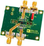
EV1HMC232ALP4 evaluation board. The design of this
evaluation board can serve as a layout recommendation for
applications.
The RF transmission lines are designed using a coplanar waveguide
(CPWG) model with a width of 16 mil and a ground spacing
(G) of 13 mil and have a characteristic impedance of 50 Ω. For
optimal RF and thermal grounding, as many plated through
vias as possible are arranged around the transmission lines and
under the exposed pad of the package.
BOARD LAYOUT
The HMC232A is a 4-layer board. The outer copper (Cu) layers
are 0.7 mil plated and are separated by dielectric materials.
Figure 19 shows the HMC232A board stack up.
G = 13mil
Figure 20 shows the top view of the populated EV1HMC232ALP4,
which is available from Analog Devices upon request (see the
Ordering Guide).
W = 16mil
0.5oz Cu (0.7mil)
0.5oz Cu (0.7mil)
0.5oz Cu (0.7mil)
T = 0.7mil
H = 10mil
RO4350
TOTAL THICKNESS
–62mil
0.5oz Cu (0.7mil)
25187-020
0.5oz Cu (0.7mil)
0.5oz Cu (0.7mil)
All RF and dc traces are routed on the top copper layer, and
the inner and bottom layers are ground planes that provide a
solid ground for the RF transmission lines. The top dielectric
material (H) is 10 mil Rogers RO4350, which allows optimal RF
performance. The middle and bottom dielectric layers provide
mechanical strength. The overall board thickness is ~62 mil,
which allows Subminiature Version A (SMA) connectors to
be connected at the board edges.
25187-021
Figure 19. HMC232A Stack Up
Figure 20. Populated EV1HMC232ALP4—Top View
The RF input and output ports (RFC, RF1, and RF2) are connected
through 50 Ω transmission lines to the SMA launchers. On the
traces of the logic control input pins (A and B), a 100 pF bypass
capacitor was used to filter high frequency noise. Figure 21
shows the suggested driver circuit.
Figure 22 and Table 7 show the typical application circuit and
bill of materials for the HMC232A, respectively.
A
VZ = 5.1V
IZT = 50µA
COMPENSATED
DEVICES
CD4689
VCC
VCC
GND
GND
TTL OR
CMOS
GaAs
SWITCH
CONTROL
B
10kΩ
–5V dc
25187-022
74HCT04 (TTL)
OR 74HC04 (CMOS)
Figure 21. Suggested Driver Circuit (VZ Is the Voltage of the Zener Diode, and IZT Is the Current of the Zener Diode.)
Rev. B | Page 10 of 12
�Data Sheet
HMC232A
J3
1
142-0701-851
NIC
GND
RF2
GND
NIC
NIC
24
23
22
21
20
19
2 3 4 5
J2
1
142-0701-851
NIC
NIC
GND
RFC
GND
NIC
U1
HMC232A
NIC
NIC
A
B
NIC
NIC
18
17
16
15
14
13
J4
J5
C1
100pF
C2
100pF
7
8
9
10
11
12
NIC
GND
RF1
GND
NIC
NIC
2 3 4 5
1
2
3
4
5
6
J6
J1
1
142-0701-851
25187-023
2 3 4 5
Figure 22. Typical Application Circuit
Table 7. Evaluation Board Bill of Materials
Component
J1 to J3
J4 to J6
C1, C2
U1
PCB
Description
SMA connectors
DC pins
100 pF capacitors, 0603 package
GaAs, SPDT switch, nonreflective, 100 MHz to 12 GHz, HMC232A
Evaluation PCB, Analog Devices, 107602, circuit board material Rogers 4350
Rev. B | Page 11 of 12
�HMC232A
Data Sheet
OUTLINE DIMENSIONS
DETAIL A
(JEDEC 95)
4.10
4.00 SQ
3.90
0.30
0.25
0.18
1
18
0.50
BSC
2.80
2.70 SQ
2.60
EXPOSED
PAD
13
TOP VIEW
PKG-004926/004942
0.90
0.85
0.80
SIDE VIEW
SEATING
PLANE
0.50
0.40
0.30
P IN 1
IN D IC ATO R AR E A OP T IO N S
(SEE DETAIL A)
24
19
6
12
BOTTOM VIEW
0.05 MAX
0.02 NOM
COPLANARITY
0.08
0.20 REF
7
0.20 MIN
FOR PROPER CONNECTION OF
THE EXPOSED PAD, REFER TO
THE PIN CONFIGURATION AND
FUNCTION DESCRIPTIONS
SECTION OF THIS DATA SHEET.
COMPLIANT TO JEDEC STANDARDS MO-220-VGGD-8
09-10-2018-C
PIN 1
INDICATOR
AREA
Figure 23. 24-Lead Lead Frame Chip Scale Package [LFCSP]
4 mm × 4 mm Body and 0.85 mm Package Height
(CP-24-16)
Dimensions shown in millimeters
ORDERING GUIDE
Model 1
HMC232ALP4E
HMC232ALP4ETR
EV1HMC232ALP4
1
Temperature Range
−40°C to +85°C
−40°C to +85°C
Package Description
24-Lead Lead Frame Chip Scale Package [LFCSP]
24-Lead Lead Frame Chip Scale Package [LFCSP]
Evaluation Board
All models are RoHS compliant parts.
©2022 Analog Devices, Inc. All rights reserved. Trademarks and
registered trademarks are the property of their respective owners.
D25187-10/22(B)
Rev. B | Page 12 of 12
Package Option
CP-24-16
CP-24-16
�