HMC245AQS16E
v01.0120
SWITCHES - MULTI-THROW - SMT
GaAs MMIC SP3T Non-REFLECTIVE
SWITCH, DC - 3.5 GHz
Typical Applications
Features
The HMC245AQS16 / 245AQS16E is ideal for:
Low Insertion Loss: 0.7 dB @ 2.0 GHz
• Basestation Infrastructure
Non-Reflective Design
• CATV / DBS
Integrated 2:3 TTL Decoder
• Wireless Local Loop
“All Off” Isolation State
• Test Equipment
Single Positive Supply: Vdd = +5V
16 Lead QSOP SMT Package
Functional Diagram
General Description
The HMC245AQS16E is a low cost non-reflective
SP3T switches in 16-lead QSOP surface mount packages. Covering DC to 3.5 GHz, the switch offers 30 to
40 dB isolation and a low insertion loss of 0.7 dB. A
2:3 TTL/CMOS compatible decoder is integrated on
the switch requiring only 2 control lines and a single
+5V bias to select each path, replacing 6 control lines
normally required by GaAs SP3T switches.
Electrical Specifications,
TA = +25° C, For TTL Control and Vdd= +5V in a 50 Ohm System
Parameter
1
Frequency
Insertion Loss
DC - 2.0 GHz
DC - 3.0 GHz
DC - 3.5 GHz
Isolation
DC - 1.0 GHz
DC - 2.0 GHz
DC - 2.5 GHz
DC - 3.5 GHz
Min.
40
35
31
26
Typ.
Max.
Units
0.7
0.8
1.1
1.0
1.3
1.5
dB
dB
dB
46
42
40
32
dB
dB
dB
dB
Return Loss
“On State”
DC - 1.5 GHz
DC - 3.5 GHz
23
17
dB
dB
Return Loss RF1 - 3
“Off State”
0.3 - 3.5 GHz
0.5 - 3.5 GHz
12
15
dB
dB
Input Power for 1 dB Compression
0.3 - 2.5 GHz
0.3 - 3.5 GHz
26
25
29
28
dBm
Input Third Order Intercept
(Two-tone Input Power = +10 dBm each tone)
0.3 - 2.5 GHz
0.3 - 3.5 GHz
44
40
48
44
dBm
Switching Characteristics
tRISE, tFALL (10/90% RF)
tON, tOFF (50% CTL to 10/90% RF)
0.3 - 3.5 GHz
40
150
ns
ns
Information furnished by Analog Devices is believed to be accurate and reliable. However, no
responsibility is assumed by Analog Devices for its use, nor for any infringements of patents or other
rights of third parties that may result from its use. Specifications subject to change without notice. No
license is granted by implication or otherwise under any patent or patent rights of Analog Devices.
Trademarks and registered trademarks are the property of their respective owners.
For price, delivery, and to place orders: Analog Devices, Inc.,
One Technology Way, P.O. Box 9106, Norwood, MA 02062-9106
Phone: 781-329-4700 • Order online at www.analog.com
Application Support: Phone: 1-800-ANALOG-D
�HMC245AQS16E
v01.0120
GaAs MMIC SP3T Non-REFLECTIVE
SWITCH, DC - 3.5 GHz
0
-0.5
-10
-1
ISOLATION (dB)
INSERTION LOSS (dB)
Isolation
0
-1.5
-2
-2.5
-20
-30
-40
-50
-60
-3
-70
0
0.5
1
1.5
2
2.5
3
3.5
0
4
0.5
1
FREQUENCY (GHz)
+25C
+85C
-40C
2
RF1
2.5
3
3.5
4
RF2
RF3
Off State Isolation
0
-5
-10
-10
-20
ISOLATION (dB)
0
-15
-20
-25
-30
-40
-50
-60
-30
-70
-35
0
0.5
1
1.5
2
2.5
3
3.5
0
4
0.5
1
FREQUENCY (GHz)
1.5
2
2.5
3
3.5
4
FREQUENCY (GHz)
RFC
RF1-3 "On"
RF1-3 "Off"
RF1
0.1 and 1 dB Input Compression Point
54
30
52
28
26
24
22
RF2
RF3
Input Third Order Intercept Point
32
INPUT IP3 (dBm)
INPUT COMPRESSION POINT (dBm)
1.5
FREQUENCY (GHz)
Return Loss
RETURN LOSS (dB)
SWITCHES - MULTI-THROW - SMT
Insertion Loss vs. Temperature
50
48
46
44
42
20
40
0
0.5
1
1.5
2
2.5
3
FREQUENCY (GHz)
3.5
4
0
0.5
1
1.5
2
2.5
3
3.5
4
FREQUENCY (GHz)
0.1 dB Compression Point
1 dB Compression Point
2
For price, delivery, and to place orders: Analog Devices, Inc., One Technology Way, P.O. Box 9106, Norwood, MA 02062-9106
Phone: 781-329-4700 • Order online at www.analog.com
Application Support: Phone: 1-800-ANALOG-D
�HMC245AQS16E
v01.0120
GaAs MMIC SP3T Non-REFLECTIVE
SWITCH, DC - 3.5 GHz
Truth Table
Vdd Range= +5 Vdc ±10%
Control Input
Vdd (Vdc)
Idd (Typ) (mA)
Idd (Max) (mA)
+5
2.2
6.0
TTL/CMOS Control Voltages
State
Bias Condition
Low
0 to +0.8 Vdc @ 0.2 µA Typ.
High
+2.0 to +5 Vdc @ 35 µA Typ.
Signal Path State
A
B
RF COM to:
Low
Low
RF1
High
Low
RF2
Low
High
RF3
High
High
All Off
For price, delivery, and to place orders: Analog Devices, Inc., One Technology Way, P.O. Box 9106, Norwood, MA 02062-9106
Phone: 781-329-4700 • Order online at www.analog.com
Application Support: Phone: 1-800-ANALOG-D
SWITCHES - MULTI-THROW - SMT
Bias Voltage & Current
3
�HMC245AQS16E
v01.0120
GaAs MMIC SP3T Non-REFLECTIVE
SWITCH, DC - 3.5 GHz
SWITCHES - MULTI-THROW - SMT
Absolute Maximum Ratings
Bias Voltage Range (Port Vdd)
+7.0 Vdc
Control Voltage Range (A & B)
-0.5V to Vdd +1 Vdc
Channel Temperature
150 °C
Thermal Resistance
Insertion Loss Path
Terminated Path
150 °C/W
297 °C/W
Storage Temperature
-65 to +150 °C
Operating Temperature
-40 to +85 °C
Maximum Input Power
Vdd = +5 Vdc
Insertion Loss Path
Terminated Path
+28.5 dBm
+23.4 dBm
ESD Sensitivity (HBM)
Class 1A
ELECTROSTATIC SENSITIVE DEVICE
OBSERVE HANDLING PRECAUTIONS
16-Lead Shrink Small Outline Package [QSOP]
(RQ-16)
Dimensions shown in inches and (millimeters)
Outline Drawing
0.197 (5.00)
0.193 (4.90)
0.189 (4.80)
16
1
9
8
0.244 (6.20)
0.236 (5.99)
0.228 (5.79)
0.010 (0.25)
0.006 (0.15)
0.069 (1.75)
0.053 (1.35)
0.065 (1.65)
0.049 (1.25)
0.010 (0.25)
0.004 (0.10)
COPLANARITY
0.004 (0.10)
0.158 (4.01)
0.154 (3.91)
0.150 (3.81)
0.025 (0.64)
BSC
0.012 (0.30)
0.008 (0.20)
SEATING
PLANE
8°
0°
0.020 (0.51)
0.010 (0.25)
0.050 (1.27)
0.016 (0.41)
0.041 (1.04)
REF
09-12-2014-A
COMPLIANT TO JEDEC STANDARDS MO-137-AB
CONTROLLING DIMENSIONS ARE IN INCHES; MILLIMETER DIMENSIONS
(IN PARENTHESES) ARE ROUNDED-OFF INCH EQUIVALENTS FOR
REFERENCE ONLY AND ARE NOT APPROPRIATE FOR USE IN DESIGN.
16-Lead Shrink Small Outline Package [QSOP]
(RQ-16)
Dimensions shown in inches and (millimeters)
Package Information
Part Number
Package Body Material
Leadframe Plating
HMC245AQS16E
RoHS-compliant Low Stress Injection Molded
Plastic Silica and Silicon Impregnated
100% Matte Tin
MSL Rating
MSL1
[1]
Package Marking [2]
H245A
XXXX
[1] Max peak reflow temperature of 260 °C
[2] 4-Digit lot number XXXX
4
For price, delivery, and to place orders: Analog Devices, Inc., One Technology Way, P.O. Box 9106, Norwood, MA 02062-9106
Phone: 781-329-4700 • Order online at www.analog.com
Application Support: Phone: 1-800-ANALOG-D
�HMC245AQS16E
v01.0120
GaAs MMIC SP3T Non-REFLECTIVE
SWITCH, DC - 3.5 GHz
Pin Descriptions
Function
Description
1, 6, 12, 14
RF3, RF2,
RF1, RFC
This pin is DC coupled and matched to 50 Ohms.
Blocking capacitors are required.
2 - 5, 7, 11, 13,
15, 16
GND
This pin must be connected to PCB RF
ground to maximize isolation.
8
Vdd
Supply Voltage +5 Vdc ±10%
9
B
See truth table and control voltage table.
10
A
See truth table and control voltage table.
Interface Schematic
For price, delivery, and to place orders: Analog Devices, Inc., One Technology Way, P.O. Box 9106, Norwood, MA 02062-9106
Phone: 781-329-4700 • Order online at www.analog.com
Application Support: Phone: 1-800-ANALOG-D
SWITCHES - MULTI-THROW - SMT
Pin Number
5
�HMC245AQS16E
v01.0120
GaAs MMIC SP3T Non-REFLECTIVE
SWITCH, DC - 3.5 GHz
SWITCHES - MULTI-THROW - SMT
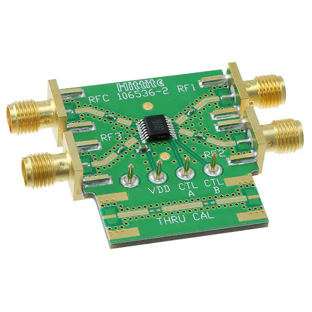
Evaluation PCB
List of Materials for Evaluation PCB EV1HMC245AQS16
Item
Description
J1 - J4
PCB Mount SMA RF Connector
J5 - J8
DC Pin
C1 - C4
100 pF Capacitor, 0402 Pkg.
C5
10k pF Capacitor, 0603 Pkg.
U1
HMC245AQS16 / 245AQS16E
SP3T Switch
PCB [2]
106536 Evaluation PCB
[1]
The circuit board used in the application should be
generated with proper RF circuit design techniques.
Signal lines at the RF port should have 50 ohm
impedance and the package ground leads should
be connected directly to the ground plane similar
to that shown above. The evaluation circuit board
shown above is available from Analog Devices
upon request.
[1] Reference this number when ordering complete evaluation PCB
[2] Circuit Board Material: Rogers 4350
6
For price, delivery, and to place orders: Analog Devices, Inc., One Technology Way, P.O. Box 9106, Norwood, MA 02062-9106
Phone: 781-329-4700 • Order online at www.analog.com
Application Support: Phone: 1-800-ANALOG-D
�