5.5 GHz to 14 GHz,
GaAs MMIC Fundamental Mixer
HMC558A
Data Sheet
FUNCTIONAL BLOCK DIAGRAM
Conversion loss: 7.5 dB typical at 5.5 GHz to 10 GHz
Local oscillator (LO) to radio frequency (RF) isolation: 45 dB
typical at 5.5 GHz to 10 GHz
LO to intermediate frequency (IF) isolation: 45 dB typical at
10 GHz to 14 GHz
Input third-order intercept (IIP3): 21 dBm typical at 10 GHz
to 14 GHz
Input P1dB: 11.5 dBm typical at 10 GHz to 14 GHz
Input second-order intercept (IIP2): 55 dBm typical at 10 GHz
to 14 GHz
Passive double-balanced topology
Wide IF bandwidth: dc to 6 GHz
12-lead ceramic leadless chip carrier package
HMC558A
LO
RF
IF
15000-001
FEATURES
Figure 1.
APPLICATIONS
Point to point microwave radios
Point to multipoint radios
Military end use
Instrumentation, automatic test equipment (ATE), and sensors
GENERAL DESCRIPTION
The HMC558A is a general-purpose, double-balanced mixer in a
leadless RoHS compliant SMT package that can be used as an
upconverter or downconverter between 5.5 GHz and 14 GHz.
This mixer is fabricated in a gallium arsenide (GaAs) metal semiconductor field effect transistor (MESFET) process, and requires
no external components or matching circuitry.
Rev. C
The HMC558A provides excellent LO to RF and LO to IF isolation
due to optimized balun structures, and operates with LO drive
levels as low as 9 dBm. The RoHS compliant HMC558A eliminates
the need for wire bonding, and is compatible with high volume
surface-mount manufacturing techniques.
Document Feedback
Information furnished by Analog Devices is believed to be accurate and reliable. However, no
responsibility is assumed by Analog Devices for its use, nor for any infringements of patents or other
rights of third parties that may result from its use. Specifications subject to change without notice. No
license is granted by implication or otherwise under any patent or patent rights of Analog Devices.
Trademarks and registered trademarks are the property of their respective owners.
One Technology Way, P.O. Box 9106, Norwood, MA 02062-9106, U.S.A.
Tel: 781.329.4700 ©2016–2018 Analog Devices, Inc. All rights reserved.
Technical Support
www.analog.com
�HMC558A
Data Sheet
TABLE OF CONTENTS
Features .............................................................................................. 1
Downconverter Performance ......................................................6
Applications ....................................................................................... 1
Upconverter Performance ............................................................9
Functional Block Diagram .............................................................. 1
Return Loss and Isolation Performance .................................. 10
General Description ......................................................................... 1
Spurious Performance ............................................................... 12
Revision History ............................................................................... 2
Theory of Operation ...................................................................... 13
Specifications..................................................................................... 3
Applications Information .............................................................. 14
Absolute Maximum Ratings ............................................................ 4
Typical Application Circuit ....................................................... 14
Thermal Resistance ...................................................................... 4
Evaluation Board Information.................................................. 14
ESD Caution .................................................................................. 4
Outline Dimensions ....................................................................... 15
Pin Configuration and Function Descriptions ............................. 5
Ordering Guide .......................................................................... 15
Interface Schematics..................................................................... 5
Typical Performance Characteristics ............................................. 6
REVISION HISTORY
7/2018—Rev. B to Rev. C
Changes to Spurious Performance Section ................................. 12
Added IF Spurious Performance Table ........................................ 12
12/2017—Rev. A to Rev. B
Changes to Figure 16 ........................................................................ 7
Changes to Ordering Guide .......................................................... 15
6/2017—Rev. 0 to Rev. A
Changes E-12-1 to E-12-4 ............................................ Throughout
Updated Outline Dimensions ....................................................... 15
Changes to Ordering Guide .......................................................... 15
11/2016—Revision 0: Initial Version
Rev. C | Page 2 of 15
�Data Sheet
HMC558A
SPECIFICATIONS
LO drive level = 15 dBm, TA = 25°C, IF = 100 MHz, upper sideband, unless otherwise noted. All measurements performed as a
downconverter.
Table 1.
Parameter
RF FREQUENCY RANGE
LO FREQUENCY RANGE
LO DRIVE LEVEL
IF FREQUENCY RANGE
PERFORMANCE AT RF = 5.5 GHz to 10 GHz
Conversion Loss
Single Sideband (SSB) Noise Figure
Input Third-Order Intercept (IIP3)
Input 1 dB Compression Point (IP1dB)
Input Second-Order Intercept (IIP2)
RF to IF Isolation
LO to RF Isolation
LO to IF Isolation
PERFORMANCE AT RF = 10 GHz to 14 GHz
Conversion Loss
SSB Noise Figure
IIP3
IP1dB
IIP2
RF to IF Isolation
LO to RF Isolation
LO to IF Isolation
Min
5.5
5.5
Typ
Max
14
14
15
DC
15
8
35
20
16
10
30
20
Rev. C | Page 3 of 15
6
Unit
GHz
GHz
dBm
GHz
7.5
7.5
17.5
10
50
16
45
35
9.5
dB
dB
dBm
dBm
dB
dB
dB
dB
8.5
10
21
11.5
55
19
40
45
10
dB
dB
dBm
dBm
dB
dB
dB
dB
�HMC558A
Data Sheet
ABSOLUTE MAXIMUM RATINGS
THERMAL RESISTANCE
Table 2.
Parameter
RF Input Power
LO Input Power
IF Input Power
IF Source/Sink Current
Maximum Junction Temperature
Continuous PDISS (T = 85°C) (Derate
5.5 mW/°C Above 85°C)
Operating Temperature Range
Storage Temperature Range
Lead Temperature Range (Soldering 60 sec)
Electrostatic Discharge (ESD) Sensitivity
Human Body Model (HBM)
Field Induced Charged Device Model
(FICDM)
Thermal performance is directly linked to printed circuit board
(PCB) design and operating environment. Careful attention to
PCB thermal design is required.
Rating
25 dBm
25 dBm
25 dBm
3 mA
175°C
495 mW
Table 3. Thermal Resistance
Package Type
E-12-41
1
−40°C to +85°C
−65°C to +150°C
−65°C to +150°C
2500 V (Class 2)
1000 V (Class C5)
θJC
180
Unit
°C/W
See JEDEC standard JESD51-2 for additional information on optimizing the
thermal impedance (PCB with 3 × 3 vias).
ESD CAUTION
Stresses at or above those listed under Absolute Maximum
Ratings may cause permanent damage to the product. This is a
stress rating only; functional operation of the product at these
or any other conditions above those indicated in the operational
section of this specification is not implied. Operation beyond
the maximum operating conditions for extended periods may
affect product reliability.
Rev. C | Page 4 of 15
�Data Sheet
HMC558A
3
NIC
NIC
HMC558A
TOP VIEW
(Not to Scale)
4
5
6
9
GND
8
RF
7
GND
NOTES
1. NIC = NO INTERNAL CONNECTION.
2. EXPOSED PAD. CONNECT THE EXPOSED PAD TO A LOW
IMPEDANCE THERMAL AND ELECTRICAL GROUND PLANE.
15000-002
2
10
GND
LO
GND
11
IF
1
12
GND
GND
NIC
PIN CONFIGURATION AND FUNCTION DESCRIPTIONS
Figure 2. Pin Configuration
Table 4. Pin Function Descriptions
Pin No.
1, 3, 4, 6, 7, 9
2
5
Mnemonic
GND
LO
IF
8
10, 11, 12
RF
NIC
EPAD
Description
Ground. See Figure 6 for the ground interface schematic.
Local Oscillator Port. This pin is ac-coupled and matched to 50 Ω. See Figure 4 for the LO interface schematic.
DC-Coupled IF. For applications not requiring operation to dc, dc block this port externally using a series
capacitor whose value is chosen to pass the necessary IF frequency range. For operation to dc, this pin
must not source or sink more than 3 mA of current, or device nonfunction and possible device failure may
result. See Figure 5 for the IF interface schematic.
RF Port. This pin is ac-coupled internally and matched to 50 Ω. See Figure 3 for the RF interface schematic.
No Internal Connection. These pins can be grounded.
Exposed Pad. Connect the exposed pad to a low impedance thermal and electrical ground plane.
Figure 5. IF Interface
Figure 3. RF Interface
GND
15000-004
LO
15000-005
IF
15000-006
RF
15000-003
INTERFACE SCHEMATICS
Figure 6. Ground Interface
Figure 4. LO Interface
Rev. C | Page 5 of 15
�HMC558A
Data Sheet
TYPICAL PERFORMANCE CHARACTERISTICS
DOWNCONVERTER PERFORMANCE
Data taken as downconverter, upper sideband (low-side LO), TA = 25°C, LO drive level = 15 dBm unless otherwise specified.
0
0
–40°C
+25°C
+85°C
–2
–4
CONVERSION GAIN (dB)
–6
–8
–10
–12
–14
–16
–8
–10
–12
–14
–16
–18
5
6
7
8
9
10
11
12
13
14
15
16
–20
7
8
9
10
11
12
13
14
15
16
32.5
30.0
27.5
27.5
25.0
25.0
22.5
22.5
20.0
20.0
15.0
12.5
17.5
15.0
12.5
10.0
10.0
7.5
7.5
5.0
9dBm
12dBm
15dBm
18dBm
20dBm
2.5
5.0
0
–40°C
+25°C
+85°C
4
5
–2.5
6
7
8
9
10
11
12
13
14
15
16
RF FREQUENCY (GHz)
–5.0
15000-108
2.5
0
0
CONVERSION GAIN (dB)
–4
–6
–8
–10
–12
–14
13
RF FREQUENCY (GHz)
14
15
16
12
13
14
15
16
16
–14
–20
15000-109
12
11
–12
–18
11
10
–10
–16
10
9
–8
–18
9
8
–6
–16
8
7
9dBm
12dBm
15dBm
18dBm
20dBm
–2
–4
7
6
Figure 11. Input IP3 vs. RF Frequency at Various LO Powers,
IF = 100 MHz
–40°C
+25°C
+85°C
6
5
RF FREQUENCY (GHz)
Figure 8. Input IP3 vs. RF Frequency at Various Temperatures,
IF = 100 MHz
–2
4
15000-111
IP3 (dBm)
17.5
–20
6
Figure 10. Conversion Gain vs. RF Frequency at Various LO Powers,
IF = 100 MHz
30.0
0
5
RF FREQUENCY (GHz)
Figure 7. Conversion Gain vs. RF Frequency at Various Temperatures,
IF = 100 MHz
CONVERSION GAIN (dB)
4
15000-110
4
15000-107
–18
RF FREQUENCY (GHz)
IP3 (dBm)
–6
15000-112
CONVERSION GAIN (dB)
–4
–20
9dBm
12dBm
15dBm
18dBm
20dBm
–2
6
7
8
9
10
11
12
13
RF FREQUENCY (GHz)
Figure 9. Conversion Gain vs. RF Frequency at Various Temperatures,
IF = 2 GHz
14
15
Figure 12. Conversion Gain vs. RF Frequency at Various LO Powers,
IF = 2 GHz
Rev. C | Page 6 of 15
�Data Sheet
18
–40°C
+25°C
+85°C
14
22.5
20.0
17.5
15.0
P1dB (dBm)
12
12.5
10.0
7.5
5.0
2.5
0
–2.5
10
8
6
4
2
6
7
8
9
10
11
12
13
14
15
16
RF FREQUENCY (GHz)
0
0
6
7
8
9
10
11
12
13
14
15
16
Figure 16. Input P1dB vs. RF Frequency at Various Temperatures,
IF = 100 MHz
25
–40°C
+25°C
+85°C
–40°C
+25°C
+85°C
20
–5.0
–7.5
NOISE FIGURE (dB)
CONVERSION GAIN (dB)
5
RF FREQUENCY (GHz)
Figure 13. Input IP3 vs. RF Frequency at Various Temperatures,
IF = 2 GHz
–2.5
4
15000-117
–5.0
–7.5
–40°C
+25°C
+85°C
16
15000-113
IP3 (dBm)
32.5
30.0
27.5
25.0
HMC558A
–10.0
–12.5
–15.0
–17.5
–20.0
15
10
5
0
1
2
3
4
5
6
7
8
9
IF FREQUENCY (GHz)
4
5
6
7
8
9
10
11
12
13
14
15
16
RF FREQUENCY (GHz)
Figure 17. SSB Noise Figure vs. RF Frequency at Various Temperatures,
IF = 100 MHz
25
9dBm
12dBm
15dBm
18dBm
20dBm
9dBm
12dBm
15dBm
18dBm
NOISE FIGURE (dB)
20
15
10
6
7
8
9
10
11
12
13
14
15
RF FREQUENCY (GHz)
16
0
4
5
6
7
8
9
10
11
12
RF FREQUENCY (GHz)
13
14
15
16
15000-123
5
15000-116
IP3 (dBm)
Figure 14. Conversion Gain vs. IF Frequency at Various Temperatures
35.0
32.5
30.0
27.5
25.0
22.5
20.0
17.5
15.0
12.5
10.0
7.5
5.0
2.5
0
–2.5
–5.0
–7.5
–10.0
–12.5
0
15000-114
–25.0
15000-120
–22.5
Figure 18. SSB Noise Figure vs. RF Frequency at Various LO Powers,
IF = 100 MHz
Figure 15. Input IP3 vs. RF Frequency at Various LO Powers,
IF = 2 GHz
Rev. C | Page 7 of 15
�Data Sheet
90
80
80
70
70
60
60
50
40
40
30
30
20
20
4
5
6
7
8
9
10
11
12
13
14
15
16
RF FREQUENCY (GHz)
0
60
IP2 (dBm)
70
50
40
9
10
11
12
13
14
15
16
50
40
30
30
20
20
10
10
8
9
10
11
12
13
14
15
16
RF FREQUENCY (GHz)
0
15000-126
7
8
80
60
6
7
90
70
0
6
Figure 21. Input IP2 vs. RF Frequency at Various LO Powers,
IF = 100 MHz
–40°C
+25°C
+85°C
80
5
RF FREQUENCY (GHz)
Figure 19. Input IP2 vs. RF Frequency at Various Temperatures,
IF = 100 MHz
90
4
9dBm
12dBm
15dBm
18dBm
20dBm
6
7
8
9
10
11
12
13
14
15
16
RF FREQUENCY (GHz)
Figure 20. Input IP2 vs. RF Frequency at Various Temperatures,
IF = 2000 MHz
Figure 22. Input IP2 vs. RF Frequency, at Various LO Powers,
IF = 2000 MHz
Rev. C | Page 8 of 15
15000-129
0
9dBm
12dBm
15dBm
18dBm
20dBm
10
–40°C
+25°C
+85°C
10
IP2 (dBm)
50
15000-128
IP2 (dBm)
90
15000-125
IP2 (dBm)
HMC558A
�Data Sheet
HMC558A
UPCONVERTER PERFORMANCE
Data taken as upconverter, upper sideband, TA = 25°C, LO drive level = 15 dBm unless otherwise specified.
–2
–4
–4
–6
–8
–10
–8
–12
–14
–14
–16
–16
–18
6
7
8
9
10
11
12
13
14
15
16
–20
27.5
32.5
27.5
22.5
20.0
20.0
17.5
17.5
IP3 (dBm)
25.0
22.5
15.0
12.5
10.0
5.0
2.5
2.5
0
–2.5
–2.5
8
9
10
11
12
13
14
15
16
RF FREQUENCY (GHz)
15000-031
0
7
10
11
12
13
14
15
16
10.0
7.5
6
9
12.5
5.0
5
8
15.0
7.5
4
7
12dBm
15dBm
18dBm
20dBm
30.0
25.0
–5.0
6
Figure 25. Conversion Gain vs. RF Frequency for Various LO Powers,
IF = 100 MHz
–40°C
+25°C
+85°C
30.0
5
RF FREQUENCY (GHz)
Figure 23. Conversion Gain vs. RF Frequency for Various Temperatures,
IF = 100 MHz
32.5
4
–5.0
4
5
6
7
8
9
10
11
12
13
14
15
16
RF FREQUENCY(GHz)
Figure 26. Input IP3 vs. RF Frequency for Various LO Powers,
IF = 100 MHz
Figure 24. Input IP3 vs. RF Frequency for Various Temperatures,
IF = 100 MHz
Rev. C | Page 9 of 15
15000-033
5
15000-030
4
15000-032
–18
RF FREQUENCY (GHz)
IP3 (dBm)
–6
–10
–12
–20
12dBm
15dBm
18dBm
20dBm
–2
CONVERSION GAIN (dB)
CONVERSION GAIN (dB)
0
–40°C
+25°C
+85°C
�HMC558A
Data Sheet
RETURN LOSS AND ISOLATION PERFORMANCE
Data taken at TA = 25°C, LO drive level = 15 dBm unless otherwise specified.
80
–40°C
+25°C
+85°C
70
ISOLATION (dB)
40
LO TO IF
40
30
20
10
10
4
5
6
7
8
9
10
11
12
13
14
15
16
LO FREQUENCY (GHz)
Figure 27. LO to RF and LO to IF Isolation vs. LO Frequency at Various
Temperatures, IF = 100 MHz
40
0
4
5
6
7
8
9
10
11
12
13
14
15
16
Figure 29. LO to RF and LO to IF Isolation vs. LO Frequency at Various
LO Powers, IF = 100 MHz
40
9dBm
12dBm
15dBm
18dBm
35
30
20
15
25
20
15
10
10
5
5
5
6
7
8
9
10
11
12
RF FREQUENCY (GHz)
13
14
15
16
0
15000-122
4
Figure 28. RF to IF Isolation vs. RF Frequency at Various Temperatures,
IF = 100 MHz
4
5
6
7
8
9
10
11
12
RF FREQUENCY (GHz)
13
14
15
16
15000-119
ISOLATION (dB)
30
25
0
LO TO IF
LO FREQUENCY (GHz)
–40°C
+25°C
+85°C
35
ISOLATION (dB)
50
20
15000-115
ISOLATION (dB)
LO TO RF
50
0
LO TO RF
60
60
30
9dBm
12dBm
15dBm
18dBm
20dBm
70
15000-118
80
Figure 30. RF to IF Isolation vs. RF Frequency at Various LO Powers,
IF = 100 MHz
Rev. C | Page 10 of 15
�Data Sheet
10
HMC558A
5
–40°C
+25°C
+85°C
5
–5
–10
–15
–20
–25
–15
–20
–25
–30
–30
–35
–35
4
5
6
7
8
9
10
11
12
13
14
15
16
LO FREQUENCY (GHz)
Figure 31. LO Return Loss vs. LO Frequency at Various Temperatures
5
0
–40
–40°C
+25°C
+85°C
–10
–15
–20
–25
–30
1.1
2.1
3.1
4.1
5.1
6.1
7.1
IF FREQUENCY (GHz)
8.1
9.1
10.1
15000-124
–35
–40
0.1
4
5
6
7
8
9
10 11 12
RF FREQUENCY (GHz)
13
14
15
16
Figure 33. RF Return Loss vs. RF Frequency at Various Temperatures,
IF = 100 MHz, LO Power = 15 dBm
–5
RETURN LOSS (dB)
–10
15000-224
RETURN LOSS (dB)
–5
15000-121
RETURN LOSS (dB)
0
–40
–40°C
+25°C
+85°C
0
Figure 32. IF Return Loss vs. IF Frequency at Various Temperatures,
LO Power = 15 dBm, LO Frequency = 11 GHz
Rev. C | Page 11 of 15
�HMC558A
Data Sheet
SPURIOUS PERFORMANCE
Mixer spurious products are measured in decibels from either
below the RF or the IF output power level. N/A means not
applicable.
IF frequency = 100 MHz at −10 dBm, LO frequency = 10.0 GHz
at 15 dBm are applied. Spur values are (M × IF) + (N × LO).
0
RF frequency = 8.1 GHz at −10 dBm, LO frequency = 8.0 GHz
at 15 dBm are applied. Spur values are (M × RF) − (N × LO), IF
output = 100 MHz.
M × RF
0
1
2
3
4
0
N/A
+10.3
+83.6
+79
+76.3
1
−1
0
+59
+84.3
+78.4
N × LO
2
+24.7
+22.7
+64
+77.8
+84.6
3
+24.4
+34.9
+58.9
+69.6
+85.7
4
+35.9
+54.3
+81.9
+75.7
+91.3
M × IF
Rev. C | Page 12 of 15
−4
−3
−2
−1
0
+1
+2
+3
+4
N/A
N/A
N/A
N/A
+69.8
N/A
N/A
N/A
1
N/A
+60
+56.5
0
−1.4
+0.3
+55.8
+60.6
N/A
N × LO
2
N/A
+77
+70.2
+29.1
+31.6
+28
+71.8
+76.8
N/A
3
N/A
+82.7
+71.8
+24.6
+27
+24.9
+74.4
+84.2
N/A
4
N/A
N/A
+74.8
+45.5
+37.5
+45.7
+75.5
+91.2
N/A
�Data Sheet
HMC558A
THEORY OF OPERATION
The HMC558A is a general-purpose double balanced mixer in a
leadless RoHS compliant SMT package that can be used as an
upconverter or downconverter between 5.5 GHz and 14 GHz. This
mixer is fabricated in a GaAs MESFET process, and requires no
external components or matching circuitry. The HMC558A
provides excellent LO to RF and LO to IF isolation due to
optimized balun structures and operates with LO drive levels as low
as 9 dBm. The RoHS compliant HMC558A eliminates the need for
wire bonding, and is compatible with high volume surface mount
manufacturing techniques.
Rev. C | Page 13 of 15
�HMC558A
Data Sheet
APPLICATIONS INFORMATION
EVALUATION BOARD INFORMATION
TYPICAL APPLICATION CIRCUIT
LO
11
1
9
2
8
3
7
4
5
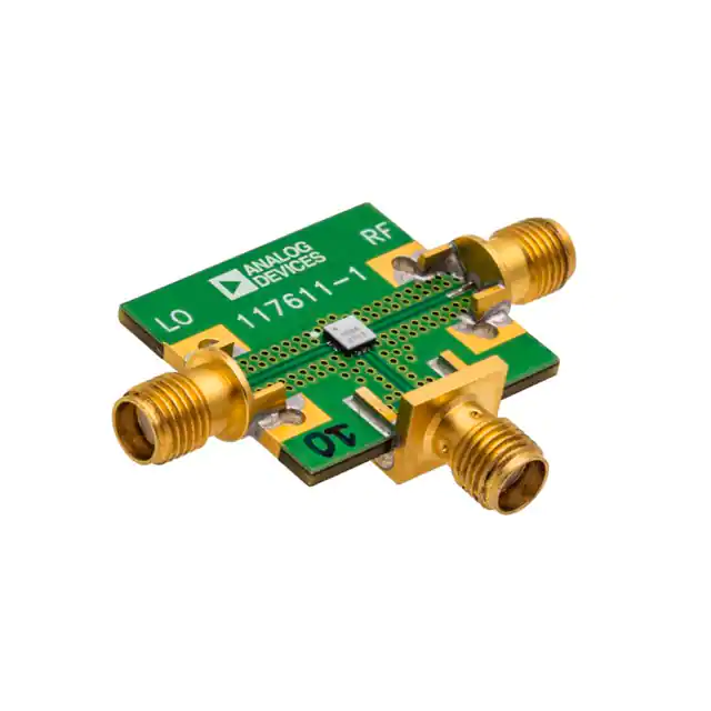
The circuit board used in an application must use RF circuit
design techniques. Signal lines must have 50 Ω impedance, and
the package ground leads and exposed pad must be connected
directly to the ground plane, similarly to that shown in Figure 35.
Use a sufficient number of via holes to connect the top and
bottom ground planes. The evaluation circuit board shown in
Figure 35 is available from Analog Devices, Inc., upon request.
10
RF
6
IF
15000-028
12
LO
Figure 34. Typical Application Circuit
RF
J2
J1
IF
U1
J3
Figure 35. HMC558A Evaluation Board Top Layer
Table 5. Bill of Materials for the EV1HMC558ALC3B Evaluation Board
Level
1
1
1
1
Item
1
2
3
4
Part Number
117611-1
104935
105192
HMC558ALC3B
Quantity
1
2
1
1
Reference Designator
J1 to J2
J3
U1
Rev. C | Page 14 of 15
Description
PCB, evaluation board
2.92 mm connector, SRI
SMA connector, Johnson
Device under test (DUT)
�Data Sheet
HMC558A
OUTLINE DIMENSIONS
0.36
0.30
0.24
0.08
BSC
10
0.50
BSC
PIN 1
12
1
9
3
7
TOP VIEW
0.90
0.80
0.70
1.60
1.50 SQ
1.40
EXPOSED
PAD
6
0.32
BSC
4
BOTTOM VIEW
1.00 REF
2.10 BSC
SIDE VIEW
FOR PROPER CONNECTION OF
THE EXPOSED PAD, REFER TO
THE PIN CONFIGURATION AND
FUNCTION DESCRIPTIONS
SECTION OF THIS DATA SHEET.
PKG-004837
SEATING
PLANE
03-02-2017-A
PIN 1
INDICATOR
3.05
2.90 SQ
2.75
Figure 36. 12-Terminal Ceramic Leadless Chip Carrier [LCC]
(E-12-4)
Dimensions shown in millimeters
ORDERING GUIDE
Model1
HMC558ALC3B
Temperature
Range
−40°C to +85°C
HMC558ALC3BTR
−40°C to +85°C
HMC558ALC3BTR-R5
−40°C to +85°C
EV1HMC558ALC3B
1
Description
12-Terminal Ceramic Leadless
Chip Carrier [LCC]
12-Terminal Ceramic Leadless
Chip Carrier [LCC]
12-Terminal Ceramic Leadless
Chip Carrier [LCC]
Evaluation PCB Assembly
Package
Option
E-12-4
Package Body
Material
Alumina Ceramic
E-12-4
Alumina Ceramic
E-12-4
Alumina Ceramic
The HMC558ALC3B, HMC558ALC3BTR, and HMC558ALC3BTR-R5 are RoHS Compliant.
©2016–2018 Analog Devices, Inc. All rights reserved. Trademarks and
registered trademarks are the property of their respective owners.
D15000-0-7/18(C)
Rev. C | Page 15 of 15
Lead Finish
Gold over
Nickel
Gold over
Nickel
Gold over
Nickel
MSL
Rating
MSL3
MSL3
MSL3
�