Data Sheet
60 GHz Millimeterwave
Transmitter, 57 GHz to 64 GHz
HMC6300
FEATURES
GENERAL DESCRIPTION
Frequency band: 57 GHz to 64 GHz
RF signal bandwidth: up to 1.8 GHz
Output power for 1 dB compression: 15 dBm
Gain: 5 dB to 35 dB
Digital and analog RF and IF gain control
Integrated frequency synthesizer
Integrated image reject filter
Partially external loop filter
Support for external local oscillator (LO)
On-chip temperature sensor
Support for 256 QAM modulation
Integrated minimum shift keying (MSK) modulator
Universal analog I/Q baseband interface
3-wire serial digital interface
65-ball, RoHS compliant, wafer level ball grid array
The HMC6300 is a complete millimeterwave transmitter
integrated circuit in a 6 mm × 4 mm RoHS compliant wafer
level ball grid array (WLBGA) that operates from 57 GHz to
64 GHz with up to 1.8 GHz modulation bandwidth.
An integrated synthesizer provides tuning in 250 MHz,
500 MHz, or 540 MHz steps with excellent phase noise to
support up to 64 QAM modulation. Optionally, an external LO
can be injected allowing for user selectable LO characteristics or
phase coherent transmit and receive operation, as well as
modulation up to 256 QAM. Support for a wide variety of
modulation formats is provided through a universal analog
baseband I/Q interface. The transmitter chip optionally
supports dedicated frequency-shift keying (FSK), minimum
shift keying (MSK), and on-off keying (OOK) modulation
formats for lower cost and lower power serial data links without
the need for high speed data converters.
APPLICATIONS
A differential output provides up to 15 dBm linear output
power into a 100 Ω load. Single-ended operation is also
supported up to 12 dBm. Together with the HMC6301, a
complete 60 GHz transceiver chipset is provided for multiple
Gbps operation in the unlicensed 60 GHz ISM band.
Small cell backhaul
60 GHz industrial, scientific, and medical (ISM) band
data transfer
Multiple Gbps data communication
WiGig/802.11ad radio
High definition video transmission
Radar/high resolution imaging
FM_PI
FM_MI
FM_PQ
FM_MQ
BB_IP
BB_IM
BB_QP
BB_QN
FUNCTIONAL BLOCK DIAGRAM
MSK
MOD
HMC6300
RFOUT_P
PA
DRIVER
IF AMP
90°
180°
RFOUT_N
×3
÷2
DIV
PFD
REFCLK_P
EXTLO_P
CP
EXTLO_N
LPF
DATA
CLK
REFCLK_N
MUX
SCANOUT
INTERFACE
SERIAL
14423-001
DETOUT
Figure 1.
Rev. C
Document Feedback
Information furnished by Analog Devices is believed to be accurate and reliable. However, no
responsibility is assumed by Analog Devices for its use, nor for any infringements of patents or other
rights of third parties that may result from its use. Specifications subject to change without notice. No
license is granted by implication or otherwise under any patent or patent rights of Analog Devices.
Trademarks and registered trademarks are the property of their respective owners.
One Technology Way, P.O. Box 9106, Norwood, MA 02062-9106, U.S.A.
Tel: 781.329.4700 ©2016–2017 Analog Devices, Inc. All rights reserved.
Technical Support
www.analog.com
�HMC6300
Data Sheet
TABLE OF CONTENTS
Features .............................................................................................. 1
ESD Caution...................................................................................7
Applications ....................................................................................... 1
Pin Configuration and Function Descriptions..............................8
General Description ......................................................................... 1
Typical Performance Characteristics ........................................... 10
Functional Block Diagram .............................................................. 1
Theory of Operation ...................................................................... 13
Revision History ............................................................................... 2
Register Array Assignment and Serial Interface .................... 13
Specifications..................................................................................... 3
Transmitter Register Array Assignments ................................ 15
Electrical Specifications, 57 GHz to 63 GHz ............................ 3
Synthesizer Settings.................................................................... 20
Electrical Specifications, 63 GHz to 64 GHz ............................ 4
Applications Information .............................................................. 22
Recommended Operating Conditions ...................................... 5
Outline Dimensions ....................................................................... 25
Power Consumption .................................................................... 6
Ordering Guide .......................................................................... 25
Absolute Maximum Ratings ............................................................ 7
REVISION HISTORY
6/2017—Rev. B to Rev. C
Change to Figure 17 ....................................................................... 14
Changes to Table 7 .......................................................................... 15
12/2016—Rev. A to Rev. B
Changes to Figure 11 and Figure 14............................................. 11
Changes to Ordering Guide .......................................................... 25
9/2016—v00.0716 to Rev. A
Updated Format .................................................................. Universal
Added Minimum Gain Parameter, Table 1 ................................... 3
Changes to Recommended Operating Conditions, Table 3 ....... 5
Changes to Figure 17 ...................................................................... 14
Added Ordering Guide Section .................................................... 25
7/2016—Revision v00.0716: Initial Version
Rev. C | Page 2 of 25
�Data Sheet
HMC6300
SPECIFICATIONS
TA = 25°C, reference frequency = 71.4286 MHz, IF bandwidth = maximum, input impedance = 100 Ω differential, output impedance =
100 Ω differential, input signal level (high modulator gain) = −36 dBm on each of the four baseband inputs, power amplifier
configuration is differential, unless otherwise noted.
ELECTRICAL SPECIFICATIONS, 57 GHz TO 63 GHz
Table 1. Electrical Specifications, 57 GHz to 63 GHz
Parameter
FREQUENCY STEP SIZE
MODULATION BANDWIDTH
GAIN
Minimum Gain
Maximum Gain
Modulator Gain Control
IF Gain Control
RF Gain Control
OUTPUT POWER
Output Power for 1 dB Compression (P1dB)
Saturated Output Power (PSAT)
Output Power for 1 dB Compression (P1dB)
Saturated Output Power (PSAT)
Detector Power Range
TEMPERATURE SENSOR RANGE
SUPPRESSION AND REJECTION
Sideband Suppression
Image Rejection
LO Suppression
Carrier Suppression
PHASE
Phase Noise
@ 100 kHz Offset
@ 1 MHz Offset
@ 10 MHz Offset
@ 100 MHz Offset
Phase-Locked Loop (PLL) Bandwidth
POWER DISSIPATION
Balanced
Single-Ended
Balanced, External LO
Test Conditions/Comments
With 71.4286 MHz reference clock
With 142.857 MHz reference clock
With 154.2857 MHz reference clock
Full I/Q bandwidth
Min
32.5
High and low gain settings
Balanced into 100 Ω
Balanced into 100 Ω
Singled-ended into 50 Ω
Singled-ended into 50 Ω
Four levels
13.9
Using internal filter
Rev. C | Page 3 of 25
10
Max
Unit
MHz
MHz
MHz
GHz
5
35
9
14
22
dB
dB
dB
dB
dB
15
17
12
14
−10 to +15
dBm
dBm
dBm
dBm
dBm
°C
−40
15
At 6/7 of RF carrier frequency (3 × LO)
Without calibration
Typ
250
500
540
1.8
+85
30
40
20
30
dBc
dBc
dBc
dBc
−75
−93
−114
−122
300
dBc/Hz
dBc/Hz
dBc/Hz
dBc/Hz
kHz
1.0
0.88
0.75
W
W
W
�HMC6300
Data Sheet
ELECTRICAL SPECIFICATIONS, 63 GHz TO 64 GHz
Table 2. Electrical Specifications, 63 GHz to 64 GHz
Parameter
FREQUENCY STEP SIZE
MODULATION BANDWIDTH
GAIN
Maximum Gain
Modulator Gain Control
IF Gain Control
RF Gain Control
OUTPUT POWER
Output Power for 1 dB Compression (P1dB)
Saturated Output Power (PSAT)
Output Power for 1 dB Compression (P1dB)
Saturated Output Power(PSAT)
Detector Power
TEMPERATURE SENSOR RANGE
SUPPRESSION AND REJECTION
Sideband Suppression
Image Rejection
LO Suppression
Carrier Suppression
PHASE
Phase Noise @ 100 kHz Offset
Phase Noise @ 1 MHz Offset
Phase Noise @ 10 MHz Offset
Phase Noise @ 100 MHz Offset
PLL Bandwidth
POWER DISSIPATION
Balanced
Single-Ended
Balanced, External LO)
Test Conditions/Comments
With 71.4286 MHz reference clock
With 142.857 MHz reference clock
With 154.2857 MHz reference clock
Full I/Q bandwidth
Min
Typ
250
500
540
1.8
30.5
32
9
14
22
dB
dB
dB
dB
15
17
12
14
−10 to +15
dBm
dBm
dBm
dBm
dBm
°C
High and low gain settings
Balanced into 100 Ω
Balanced into 100 Ω
Singled-ended into 50 Ω
Singled-ended into 50 Ω
Four levels
13.9
−40
15
At 6/7 of RF carrier frequency (3 × LO)
Without calibration
Using internal filter
Rev. C | Page 4 of 25
10
Max
+85
Unit
MHz
MHz
MHz
GHz
30
40
20
30
dBc
dBc
dBc
dBc
−75
−93
−114
−122
300
dBc/Hz
dBc/Hz
dBc/Hz
dBc/Hz
kHz
1.0
0.88
0.75
W
W
W
�Data Sheet
HMC6300
RECOMMENDED OPERATING CONDITIONS
Table 3.
Parameter
POWER SUPPLY
Power Amplifier
Driver
Divider
Mixer
Intermediate Frequency
Radio Frequency Variable Gain Amplifier
Tripler
VCO
Digital Circuit
Synthesizer
INPUT VOLTAGE RANGE
Serial Digital Interface
Logic High
Logic Low
REFERENCE CLOCK
Reference Clock, Positive
Reference Clock, Negative
BASEBAND I/Q
In-Phase Baseband Input
Negative
Positive
Quadrature Baseband Input
Negative
Positive
BASEBAND I/Q, COMMON MODE
In-Phase Baseband Input
Negative
Positive
Quadrature Baseband Input
Negative
Positive
MSK DATA
MSK In-Phase Input
Negative (Minus)
Positive
MSK Quadrature Input
Negative (Minus)
Positive
MSK COMMON MODE
ANALOG GAIN CONTROL
RF Variable Gain Amplifier
IF Variable Gain Amplifier
EXTERNAL LO
Positive
Negative
Symbol
Min
Typ
Max
Unit
VCCPAN, VCCPAP
VDDPA
VCCDRV
VCCDIV
VCCMIX
VCCIF
VCCRFVGA
VCCTRIP
VCCVCO
VDDD
VDDSYN
3.9
2.565
2.565
2.565
2.565
2.565
2.565
2.565
2.565
1.3
1.3
4
2.7
2.7
2.7
2.7
2.7
2.7
2.7
2.7
1.35
1.35
4.1
2.835
2.835
2.835
2.835
2.835
2.835
2.835
2.835
1.48
1.48
V dc
V dc
V dc
V dc
V dc
V dc
V dc
V dc
V dc
V dc
V dc
0.9
−0.05
1.2
+0.1
1.4
+0.3
V
V
DATA, ENABLE, CLK, RESET
REFCLK_P
3.3 V or 2.5 V LVPECL/LVDS,
1.2 V CMOS
3.3 V or 2.5 V LVPECL/LVDS,
1.2 V CMOS
REFCLK_N
V
V
V
V
BB_IM
BB_IP
5
5
100
100
750
750
mV p-p
mV p-p
BB_QN
BB_QP
5
5
100
100
750
750
mV p-p
mV p-p
BB_IM
BB_IP
1.6
1.6
V
V
BB_QN
BB_QP
1.6
1.6
V
V
FM_MI
FM_PI
200
200
500
500
750
750
mV p-p
mV p-p
FM_MQ
FM_PQ
200
200
500
500
1.1
750
750
mV p-p
mV p-p
V
ANARFVGA
ANAIFVGA
0.1
0.1
1.1
1.1
2.5
2.5
V
V
EXTLO_P
EXTLO_N
0
0
3
3
5
5
dBm
dBm
Rev. C | Page 5 of 25
�HMC6300
Data Sheet
Parameter
DRAIN CURRENT
1.35 V
2.7 V
4.0 V (Balanced)
4.0 V (Singled-Ended)
Symbol
Min
Typ
10
277
58
29
POWER CONSUMPTION
Table 4.
Parameter
VCCPAN
VCCPAP
VCCDRV
VCCDIV
VCCMIX
VCCIF
VCCRFVGA
VCCTRIP
VCCVCO
VCCPA
VCCD
VCCSYN
Voltage (V)
4.0
4.0
2.7
2.7
2.7
2.7
2.7
2.7
2.7
2.7
1.35
1.35
Typical Current (mA)
29
29
32
46
32
31
20
56
52
8
0.08
10
Rev. C | Page 6 of 25
Typical Power Consumption (mW)
116
116
86
124
86
84
54
151
140
22
0.1
13
Max
Unit
mA
mA
mA
mA
�Data Sheet
HMC6300
ABSOLUTE MAXIMUM RATINGS
Table 5.
Parameter
VCCDRV
VCCDIV
VCCPAN, VCCPAP
VCCVCO
VCCRFVGA
VCCIF
VCCMIX
VCCTRIP
VDDSYN
VDDPA
VDDD
Serial Digital Interface Input Voltage
Thermal Resistance (RTH), Junction to
Ground Paddle
Baseband Inputs: BB, FM (Each)
Storage Temperature
Operating Temperature
Reflow Temperature (Maximum Peak)
ESD Sensitivity, Charged Device Model
(CDM)
Rating
2.85 V
2.85 V
4.2 V
2.85 V
2.85 V
2.85 V
2.85 V
2.85 V
1.6 V
2.85 V
1.6 V
1.5 V
9.57°C
Stresses at or above those listed under Absolute Maximum
Ratings may cause permanent damage to the product. This is a
stress rating only; functional operation of the product at these
or any other conditions above those indicated in the operational
section of this specification is not implied. Operation beyond
the maximum operating conditions for extended periods may
affect product reliability.
ESD CAUTION
0.75 V p-p
−55°C to +150°C
−40°C to 85°C
260°C
Class C3 (250 V)
Rev. C | Page 7 of 25
�HMC6300
Data Sheet
PIN CONFIGURATION AND FUNCTION DESCRIPTIONS
HMC6300
1
2
3
4
5
6
7
8
9
10
11
12
A
DETOUT
REFOUT
VCCDRV
BB_QN
BB_QP
BB_IM
BB_IP
FM_MQ
FM_PQ
FM_MI
FM_PI
VCCDIV
B
VCCPAP
RFB
VCCMIX
VCCIF
GND
GND
GND
GND
EXTFIL_P
EXTFIL_N
VCCDIV
VCCDIV
GND
VSSDIV
VSSLPF_BIAS_PLL
RFOUT_P
VSSCP_PFD
REFCLK_P
REFOUT_N
VSSREF_DIG
REFCLK_N
GND
VREGOUT
VDDSYN
C
D
E
F
G
VCCPAN
VDDPA
VCCRFVGA
SCANOUT
VDDD
RESET
VCCTRIP
VSSVCO
VSSVCO
VCCVCO
VCCVCO
VCORCAP
H
VCCDRV
ANARFVGA
DATA
ENABLE
CLK
ANAIFVGA
VSSVCO
EXTLO_N
EXTLO_P
VSSVCO
VSSVCO
VSSVCO
GROUND AREA
Figure 2. Pin Configuration Diagram
Table 6. Pin Function Descriptions
Pin No.
A1
A2
A3, H1
A4
A5
A6
A7
A8
A9
A10
A11
A12, B11, B12
B1
B2
B3
B4
B5 to B8, C1, F1
Mnemonic
DETOUT
REFOUT
VCCDRV
BB_QN
BB_QP
BB_IM
BB_IP
FM_MQ
FM_PQ
FM_MI
FM_PI
VCCDIV
VCCPAP
RFB
VCCMIX
VCCIF
GND
Description
Detector Output (0.6 V dc to 2.6 V dc).
Detector Reference Output (0.6 V dc).
Driver Power Supply (2.7 V dc).
Quadrature Negative Baseband Input. This pin is dc-coupled and matched to 50 Ω.
Quadrature Positive Baseband Input. This pin is dc-coupled and matched to 50 Ω.
In-Phase Negative Baseband Input. This pin is dc-coupled and matched to 50 Ω.
In-Phase Positive Baseband Input. This pin is dc-coupled and matched to 50 Ω.
FSK Negative (Minus) Quadrature Input. This pin is dc-coupled and matched to 50 Ω.
FSK Positive Quadrature Input. This pin is dc-coupled and matched to 50 Ω.
FSK Negative (Minus) In-Phase Input. This pin is dc-coupled and matched to 50 Ω.
FSK Positive In-Phase Input. This pin is dc-coupled and matched to 50 Ω.
Divider Power Supply (2.7 V dc).
Power Amplifier Power Supply (4.0 V dc).
Detector Circuit Feedback.
Mixer Power Supply (2.7 V dc).
IF Power Supply (2.7 V dc).
Analog Ground Connect.
Rev. C | Page 8 of 25
14423-002
TOP VIEW
(BALL SIDE DOWN)
�Data Sheet
HMC6300
Pin No.
B9
B10
C11
C12
D1
Mnemonic
EXTFIL_P
EXTFIL_N
VSSDIV
VSSLPF_BIAS_PLL
RFOUT_P
D11
D12
E1
VSSCP_PFD
REFCLK_P
RFOUT_N
E11
E12
F11
F12
G1
G2
G3
G4
G5
G6
G7
G8, G9, H7, H10 to H12
G10, G11
G12
H2
H3
H4
H5
H6
H8
H9
VSSREF_DIG
REFCLK_N
VREGOUT
VDDSYN
VCCPAN
VDDPA
VCCRFVGA
SCANOUT
VDDD
RESET
VCCTRIP
VSSVCO
VCCVCO
VCORCAP
ANARFVGA
DATA
ENABLE
CLK
ANAIFVGA
EXTLO_N
EXTLO_P
Description
External PLL Filter (Positive).
External PLL Filter (Negative).
Digital Ground for the Synthesizer.
Digital Ground for Synthesizer.
Radio Frequency Output (Positive). This pin is ac-coupled and is differentially matched to
100 Ω. This output port is disabled when single-ended output is selected.
Digital Ground for Synthesizer.
External Reference Clock (Positive). This pin can be dc or ac matched to 50 Ω.
Radio Frequency Output (Negative). This pin is ac coupled and is diff matched to 100 Ω.
This pin is used if single-ended output is selected.
Digital Ground for Synthesizer.
External Reference Clock (Negative). This pin can be dc or ac matched to 50 Ω.
VCO Regulator Output.
Synthesizer Power Supply (1.3 V dc).
Power Amplifier Power Supply (4.0 V dc).
Power Amplifier Power Supply (2.7 V dc).
RF VGA Power Supply (2.7 V dc).
Serial Digital Interface Output (1.2 V CMOS).
Digital Circuits Power Supply (1.3 V dc).
Serial Digital Interface Reset (1.2 V CMOS).
Tripler Power Supply (2.7 V dc).
Digital Ground for the VCO.
VCO Power Supply (2.7 V dc).
External Capacitor Connection for the VCO Regulator.
0.1 V to 2.4 V RF VGA Analog Control. Connect Pin H2 to 2.7 V dc for digital control.
Serial Digital Interface Data (1.2 V CMOS).
Serial Digital Interface Enable (1.2 V CMOS).
Serial Digital Interface Clock (1.2 V CMOS).
0.1 V to 2.4 V IF VGA Analog Control. Connect Pin H6 to 2.7 V dc for digital control.
External LO (Negative) Input.
External LO (Positive) Input.
Rev. C | Page 9 of 25
�HMC6300
Data Sheet
TYPICAL PERFORMANCE CHARACTERISTICS
–2
45
0
40
2
ATTENUATION (dB)
50
30
25
4
6
8
10
+85°C
+25°C
–40°C
10
57
58
+85°C
+25°C
–40°C
12
59
60
61
63
62
64
FREQUENCY (GHz)
14
2.00
14423-003
15
Figure 3. Maximum Gain vs. Frequency over Temperature, IF and RF
Attenuation = 0 dBm
1.75
1.50
1.25
1.00
0.75
0.50
0.25
Figure 6. IF Attenuation vs. Analog Control Voltage over Temperature,
Measurement Taken at 60 GHz, RF Attenuation = 0 dBm
0
0
2
+85°C
+25°C
–40°C
2
4
4
ATTENUATION (dB)
8
10
12
14
16
6
8
10
12
18
14
20
+85°C
+25°C
–40°C
24
2.2
2.0
1.8
16
1.5
1.3
1.0
0.8
0.5
0.3
0
ANALOG CONTROL VOLTAGE (V)
18
14423-004
22
0
1
2
3
4
5
7
6
9
8
10 11 12 13 14 15
DIGITAL SETTING
Figure 4. RF Attenuation vs. Analog Control Voltage over Temperature,
Measurement Taken at 60 GHz, IF Attenuation = 0 dBm
14423-007
ATTENUATION (dB)
6
Figure 7. IF Attenuation vs. Digital Setting over Temperature,
Measurement Taken at 60 GHz, RF Attenuation = 0 dBm
20
0
+85°C
+25°C
–40°C
2
18
16
4
14
P1dB (dBm)
6
8
10
12
10
8
12
6
14
4
16
+85°C
+25°C
–40°C
2
18
0
1
2
3
4
5
6
7
8
9
10 11 12 13 14 15
DIGITAL SETTING
Figure 5. RF Attenuation vs. Digital Setting over Temperature,
Measurement Taken at 60 GHz, IF Attenuation = 0 dBm
0
57
14423-005
ATTENUATION (dB)
0
ANALOG CONTROL VOLTAGE (V)
14423-006
20
58
59
60
61
62
63
64
FREQUENCY (GHz)
Figure 8. Output P1dB vs. Frequency over Temperature, IF and RF
Attenuation = 0 dBm
Rev. C | Page 10 of 25
14423-008
GAIN (dB)
35
�Data Sheet
HMC6300
25
25
+85°C
+25°C
–40°C
23
21
20
17
15
OIP3 (dBm)
PSAT (dBm)
19
15
13
10
11
5
+85°C
+25°C
–40°C
7
58
59
60
61
62
63
64
FREQUENCY (GHz)
0
57
14423-009
+85°C
+25°C
–40°C
SIDEBAND SUPPRESSION (dBc)
63
64
–35
–40
–45
–50
–35
–40
–45
–50
+85°C
+25°C
–40°C
–55
59
60
61
62
63
64
FREQUENCY (GHz)
–60
57
14423-010
58
–70
–70
–80
–80
PHASE NOISE (dBc/Hz)
–60
–110
–120
+85°C
+25°C
–40°C
100K
1M
10M
FREQUENCY (Hz)
100M
1G
Figure 11. Phase Noise vs. Frequency Offset over Temperature, Internal
LO, Measurement Taken at 60 GHz
61
62
63
64
–90
–100
–110
–120
–130
14423-011
10k
60
Figure 13. Sideband Suppression vs. Frequency over Temperature, IF and
RF Attenuation = 0 dBm
–60
–100
59
FREQUENCY (GHz)
Figure 10. Carrier Suppression vs. Frequency over Temperature, IF and RF
Attenuation = 0 dBm
–90
58
14423-013
CARRIER SUPPRESSION (dBc)
62
–30
–55
PHASE NOISE (dBc/Hz)
61
–25
–30
–140
1k
60
Figure 12. OIP3 vs. Frequency over Temperature, Total POUT = 0 dBm, IF
and RF Attenuation = 0 dBm
–25
–130
59
FREQUENCY (GHz)
Figure 9. Output Saturated Power (PSAT) vs. Frequency over Temperature,
IF and RF Attenuation = 0 dBm
–60
57
58
–140
1k
+85°C
+25°C
–40°C
10k
100K
1M
10M
FREQUENCY (Hz)
100M
1G
14423-014
5
57
14423-012
9
Figure 14. Phase Noise vs. Frequency Offset over Temperature, External
LO, Measurement Taken at 60 GHz
Rev. C | Page 11 of 25
�HMC6300
Data Sheet
16
8
SENSOR READING
OUTPUT VOLTAGE (V)
10
1
0.1
4
2
0
2
4
6
8
10
12
14
OUTPUT POWER (dBm)
16
18
20
1
–40 –30 –20 –10
14423-015
0.01
0
10
20
30
40
50
60
70
80
TEMPERATURE (°C)
Figure 15. Detector Output Voltage vs. Output Power over Temperature,
Measurement Taken at 60 GHz, and 1.15 kΩ Connecting DETOUT and RFB Pins
Rev. C | Page 12 of 25
Figure 16. Temperature Sensor Reading vs. Temperature
90
14423-016
+85°C
+25°C
–40°C
�Data Sheet
HMC6300
THEORY OF OPERATION
An integrated frequency synthesizer creates a low phase noise LO
between 16.3 GHz and 18.3 GHz. The step size of the synthesizer
equates to 250 MHz steps at RF when used with a 71.42857 MHz
reference crystal or 500 MHz if used with a 142.857 reference
crystal. To support IEEE channels (ISM band) with a 540 MHz
step size, use a 154.2857 MHz reference crystal.
If the chip is configured for I/Q baseband input, these signals
are quadrature modulated onto an 8 GHz to 9.1 GHz sliding IF
using the synthesized LO divided by two. There are also options
to input AM/FM/FSK/MSK waveforms directly to the on-chip
IF modulators. The IF signal is then filtered and amplified with
14 dB of variable gain, then mixed with three times the LO
frequency to upconvert to an RF frequency between 57 GHz
and 64 GHz.
Integrated notch filters attenuate the lower mixing product at
40 GHz to 46 GHz. Three RF amplifier stages provide gain to
allow up to 15 dBm of linear and differential output power with
22 dB of variable gain. IF and RF gain can be controlled using
either analog voltages or the digital SPI. For lower power consumption, half of the power amplifier can be disabled to run in a
single-ended configuration; this drops the output power by 3 dB.
An on-chip power detector can be used to monitor the rms
output power. The detector output pin (DETOUT) is connected
through an external resistor to the RFB pin. A resistor value of
1.15 kΩ is recommended for optimal coverage up to the P1dB
point of the transmitter. The REFOUT pin provides the reference
voltage for the detector, and the difference between DETOUT and
REFOUT is used to estimate the output power.
The phase noise and quadrature balance of the on-chip synthesizer
is sufficient to support up to 64 QAM modulation. For higher
order modulation (up to 256 QAM or less than 250 MHz step
size), the HMC6300 can be operated using an external LO.
The HMC6300 transmitter is ideal for FDD operation together
with the HMC6301 receiver chip. However, both devices can
support TDD operation by enabling and disabling the circuits.
All of the enables are placed in register array, four of which
allow for full chip enable or disable in one SPI write.
There are no special power sequencing requirements for the
HMC6300; all voltages are to be applied simultaneously.
REGISTER ARRAY ASSIGNMENT AND SERIAL
INTERFACE
The register arrays for both the transmitter and receiver are
organized into 32 rows of 8 bits. Using the serial interface, the
arrays are written or read one row at a time, as shown in Figure 17
and Figure 18, respectively. Figure 17 shows the sequence of
signals on the ENABLE, CLK, and DATA lines to write one
8-bit row of the register array. The ENABLE line goes low, the
first of 18 data bits (Bit 0) is placed on the DATA line, and 2 ns
or longer after the DATA line stabilizes, the CLK line goes high
to clock in Data Bit 0. The DATA line should remain stable for
at least 2 ns after the rising edge of CLK.
A write operation requires 18 data bits and 18 clock pulses, as
shown in Figure 17. The 18 data bits contain the 8-bit register
array row data (LSB is clocked in first), followed by the register
array row address (ROW 0 through ROW 23, 000000 to 001111,
LSB first), the read/write bit (set to 1 to write), and finally the
Tx Chip Address 110, LSB first).
The Tx IC supports a serial interface running up to several
hundred megahertz, and the interface is 1.2 V CMOS levels.
Note that the register array row address is six bits, but only four
are used to designate 32 rows, the two MSBs are 0.
After the 18th clock pulse of the write operation, the ENABLE
line returns high to load the register array on the IC; prior to
the rising edge of the ENABLE line, no data is written to the
array. The CLK line should have stabilized in the low state at
least 2 ns prior to the rising edge of the ENABLE line.
Rev. C | Page 13 of 25
�HMC6300
Data Sheet
TIME = 0
ENABLE
1
18
CLK
1
2
3
4
5
6
7
8
9
10
11
12
13
14
15
LSB
14423-017
MSB
LSB
MSB
17
CHIP
ADDRESS
ARRAY ADDRESS
LSB
DATA
16
MSB
0
DATA
R/W = 1
Figure 17.Timing Diagram for Writing a Row of the Transmitter Serial Interface
TIME = 0
ENABLE
1
27
CLK
0
1
2
3
4
5
6
7
8
9
10 11 12 13 14 15 16 17
DATA
0
1
2
3
4
5
6
7
SCAN OUT
Figure 18. Timing Diagram for Reading a Row of the Transmitter Serial Interface
Rev. C | Page 14 of 25
14423-018
R/W = 0
MSB
READ DATA
LSB
MSB
MSB
LSB
LSB
CHIP
ADDRESS
ARRAY ADDRESS
MSB
LSB
WRITE DATA =
(xxxxxxxx)
�Data Sheet
HMC6300
TRANSMITTER REGISTER ARRAY ASSIGNMENTS
In the following table, N/A means not applicable. All register arrays are read/write, unless otherwise indicated.
Table 7. Transmitter Register Array Assignments
Register Array Row
and Bit
ROW0
ROW1
ROW1, Bit 7
ROW1, Bit 6
ROW1, Bit 5
ROW1, Bit 4
ROW1, Bit 3
ROW1, Bit 2
ROW1, Bit 1
ROW1, Bit 0
ROW2
ROW2, Bit 7
ROW2, Bit 6
ROW2, Bit 5
ROW2, Bit 4
ROW2, Bit 3
ROW2, Bit 2
ROW2, Bit 1
ROW2, Bit 0
ROW3
ROW3, Bit 7
ROW3, Bit 6
ROW3, Bit 5
ROW3, Bit 4
ROW3, Bit 3
ROW3, Bit 2
ROW3, Bit 1
ROW3, Bit 0
ROW4
ROW4, Bit 7
ROW4, Bit 6
ROW4, Bit 5
ROW4, Bit 4
ROW4, Bit 3
ROW4, Bit 2
ROW4, Bit 1
ROW4, Bit 0
ROW5
ROW5, Bit 7
ROW5, Bit 6
ROW5, Bit 5
ROW5, Bit 4
ROW5, Bit 3
ROW5, Bit 2
ROW5, Bit 1
ROW5, Bit 0
Internal Signal Name
N/A
Signal Function
Not used.
pa_sel_vgbs
pa_sel_vgbs
pa_sel_vgbs
pa_sel_vgbs
pa_sel_vref
pa_sel_vref
pa_sel_vref
pa_sel_vref
Controls the regulator for the base voltage of the power amplifier output
transistors.
ROW1, Bits[7:3] = 1100 for normal operation.
pa_sel_alc_dac
pa_sel_alc_dac
pa_sel_alc_dac
pa_sel_alc_dac
pa_sep_pa_pwrdn_fast
pa_pwrdwn_fast
pa_se_sel
Factory diagnostics; ROW2.
Bits[7:4] = 1111 for normal operation.
power_det_pwrdn
Controls the bias current for the power amplifier output transistors.
ROW1, Bits[3:0] = 1010 for normal operation.
Active high for normal operation.
Active high for normal operation.
Control for Tx output interface; active low for differential Tx output; active high for
Tx single-ended output.
Active low to enable Tx power detector.
driver_bias
driver_bias
driver_bias
driver_bias2
driver_bias2
driver_bias2
en_ifmix_HiCG
en_tempflash
Controls the bias current for the power amplifier driver.
ROW3, Bits[7:5] = 111 for normal operation.
driver_pwrdn
upmixer_pwrdn
ifvga_pwrdn
divider_pwrdn
pa_pwrdn
rfvga_pwrdn
tripler_pwrdn
if_upmixer_pwrdn
Active high to power down the driver amplifier.
Active high to power down the upmixer.
Active high to power down the IF VGA.
Active high to power down the divider.
Active high to power down the power amplifier.
Active high to power down the RF VGA.
Active high to power down the tripler.
Active high to power down the IF upmixer.
tripler_bias
tripler_bias
tripler_bias
tripler_bias
tripler_bias
tripler_bias
tripler_bias
tripler_bias
Controls bias of frequency tripler.
ROW5, Bits[7:0] = 11111111 for normal operation.
Controls the bias current for the Power Amplifier Predriver 2.
ROW3, Bits[4:2] = 101 for normal operation.
Active high to enable high gain mode in IF mixer.
Active high to enable temperature sensor.
Rev. C | Page 15 of 25
�HMC6300
Register Array Row
and Bit
ROW6
ROW6, Bit 7
ROW6, Bit 6
ROW6, Bit 5
ROW6, Bit 4
ROW6, Bit 3
ROW6, Bit 2
ROW6, Bit 1
ROW6, Bit 0
ROW7
ROW7, Bit 7
ROW7, Bit 6
ROW7, Bit 5
ROW7, Bit 4
ROW7, Bit 3
ROW7, Bit 2
ROW7, Bit 1
ROW7, Bit 0
ROW8
ROW8, Bit 7
ROW8, Bit 6
ROW8, Bit 5
ROW8, Bit 4
ROW8, Bit 3
ROW8, Bit 2
ROW8, Bit 1
ROW8, Bit 0
ROW9
ROW9, Bit 7
ROW9, Bit 6
ROW9, Bit 5
Data Sheet
Internal Signal Name
Signal Function
tripler_bias
tripler_bias
tripler_bias
tripler_bias
tripler_bias
tripler_bias
N/A
Controls bias of frequency tripler.
ROW6, Bits[7:2] = 111011 for normal operation.
ifvga_vga_adj
ifvga_vga_adj
ifvga_vga_adj
ifvga_vga_adj
ifvga_tune
ifvga_tune
ifvga_tune
ifvga_tune
IF variable gain amplifier gain control bits.
ROW7, Bits[7:4] = 0000 is highest gain and 1101 is lowest gain.
Attenuation is ≈ 1.3 dB per step, ≈ 17 dB maximum.
ifvga_bias
ifvga_bias
ifvga_bias
ifvga_bias
if_upmixer_tune
if_upmixer_tune
if_upmixer_tune
if_upmixer_tune
Controls the bias current of the IF variable gain amplifier.
ROW8, Bits[7:4] = 1000 for normal operation.
ifvga_q_cntrl
ifvga_q_cntrl
ifvga_q_cntrl
Controls the Q of the IF filter in the baseband to IF upmixer.
ROW9, Bits[7:5] = 000 for the highest Q and highest gain.
To reduce Q and widen bandwidth, increment ROW9, Bits[7:5] in sequence, as
follows:
001
100
101
111
Not used.
ROW9, Bit 4
ROW9, Bit 3
ROW9, Bit 2
ROW9, Bit 1
ROW9, Bit 0
ROW10
ROW10, Bit 7
N/A
ROW10, Bit 6
ROW10, Bit 5
ROW10, Bit 4
ROW10, Bit 3
ROW10, Bit 2
if_refsel
bg_monitor
enDig_IFVGA_Gain_Control
ipc_pwrdn
if_bgmux_pwrdn
ROW10, Bit 1
ROW10, Bit 0
ROW11
upmix_cal_pwrdn
TempSensor_pwrdn
enable_FM
Not used.
Controls the tuning of the IF filter for the variable gain amplifier.
ROW7, Bits[3:0] = 1111 for normal operation.
Controls the tuning of the IF filter for the IF to RF upmixer.
ROW8, Bits[3:0] = 1111 for normal operation.
Active high to enable FSK/MSK modulation inputs.
0 = normal I/Q operation.
Reserved for diagnostic purposes.
ROW10, Bits[6:5] = 10 for normal operation.
Active high to enable digital control of IFVGA gain.
Active high to power down the chip current reference generator.
Active high to power down one of three on-chip band gap references (IF) and
associated mux.
Active high to power down upmixer calibration.
Active high to power down the temperature sensor.
Rev. C | Page 16 of 25
�Data Sheet
Register Array Row
and Bit
ROW11, Bit 7
ROW11, Bit 6
ROW11, Bit 5
ROW11, Bit 4
HMC6300
Internal Signal Name
RFVGAgain
RFVGAgain
RFVGAgain
RFVGAgain
ROW11, Bit 3
ROW11, Bit 2
ROW11, Bit 1
ROW11, Bit 0
ROW12
ROW12, Bit 7
ROW12, Bit 6
ROW12, Bit 5
ROW12, Bit 4
ROW12, Bit 3
ROW12, Bit 2
ROW12, Bit 1
ROW12, Bit 0
ROW13
ROW14
ROW15
ROW16
ROW16, Bit 7
enRFVGA_Ana
RFVGA_ICtrl
RFVGA_ICtrl
RFVGA_ICtrl
ROW16, Bit 6
en_cpShort
ROW16, Bit 5
ROW16, Bit 4
ROW16, Bit 3
en_cpCMFB
en_cp_dump
en_cpTRIST
ROW16, Bit 2
ROW16, Bit 1
ROW16, Bit 0
en_cp
en_synth_LDO
enbar_synthBG
ROW17
ROW17, Bit 7
ROW17, Bit 6
en_lockd_clk
en_test_divOut
ROW17, Bit 5
ROW17, Bit 4
ROW17, Bit 3
ROW17, Bit 2
en_vtune_flash
en_reBuf_DC
en_refBuf
en_stick_div
ROW17, Bit 1
en_FBDiv_cml2cmos
ROW17, Bit 0
ROW18
ROW18, Bit 7
ROW18, Bit 6
ROW18, Bit 5
en_FBDiv
ROW18, Bit 4
en_extLO
upmix_cal
upmix_cal
upmix_cal
upmix_cal
upmix_cal
upmix_cal
upmix_cal
upmix_cal
N/A
N/A
N/A
byp_synth_LDO
N/A
en_nb250m
byp_vco_LDO
Signal Function
RF variable gain amplifier control bits.
ROW11, Bits[7:4] gain settings as follows:
0000 = highest gain.
1111 = lowest gain.
Attenuation is ≈ 1.3 dB/step, ≈ 17 dB maximum.
Active high to enable analog gain control of RFVGA.
Controls bias current of RF variable amplifier.
ROW11, Bits[2:0] = 011 for normal operation.
3 × LO feedthrough calibration of RF upmixer.
ROW12, Bits[7:0] = 01100100 for uncalibrated operation.
Not used.
Not used.
Not used.
Factory diagnostics.
0 = normal operation.
Factory diagnostics.
0 = normal operation.
Enables CMFB circuit for charge pump, set to 1 when synthesizer is in use.
Enables auxiliary circuit for charge pump, set to 1 when synthesizer is in use.
Factory Diagnostics.
0 = normal operation.
Enables charge pump, set to 1 when synthesizer is in use.
Enables LDO for synthesizer, set to 1 when synthesizer is in use.
Factory diagnostics.
0 = normal operation.
Enables lock detector for synthesizer, set to 1 when synthesizer is in use.
Factory diagnostics.
0 = normal operation.
Enables flash ADCs for VCO vtune port, set to 1 when synthesizer is in use.
Enables dc coupling for reference clock buffer.
Enables reference clock buffer, set to 1 when synthesizer is in use.
Factory diagnostics.
0 = normal operation.
Enables auxiliary circuit for the feedback divider chain, set to 1 when synthesizer is
in use.
Enables feedback divider chain, set to 1 when synthesizer is in use.
Not used.
Active high to enable, 250 MHz channel step size.
Factory diagnostics.
0 = normal operation.
Enables external LO, set to 0 when synthesizer is in use.
Rev. C | Page 17 of 25
�HMC6300
Data Sheet
Register Array Row
and Bit
ROW18, Bit 3
Internal Signal Name
en_vcoPk
ROW18, Bit 2
ROW18, Bit 1
ROW18, Bit 0
en_vco
en_vco_reg
enbar_vcoGB
ROW19
ROW19, Bit 7
ROW19, Bit 6
ROW19, Bit 5
ROW19, Bit 4
ROW19, Bit 3
ROW19, Bit 2
ROW19, Bit 1
ROW19, Bit 0
ROW20
ROW20, Bit 7
ROW20, Bit 6
ROW20, Bit 5
ROW20, Bit 4
ROW20, Bit 3
ROW20, Bit 2
ROW20, Bit 1
ROW20, Bit 0
ROW21
ROW21, Bit 7
ROW21, Bit 6
ROW21, Bit 5
ROW21, Bit 4
ROW21, Bit 3
ROW21, Bit 2
ROW21, Bit 1
ROW21, Bit 0
ROW22
ROW22, Bit 7
ROW22, Bit 6
ROW22, Bit 5
ROW22, Bit 4
ROW22, Bit 3
ROW22, Bit 2
ROW22, Bit 1
ROW22, Bit 0
Signal Function
Factory diagnostics.
0 = normal operation.
Enables internal VCO, set to 1 when synthesizer is in use.
Enables internal regulator for VCO, set to 1 when synthesizer is in use.
Factory diagnostics.
0 = normal operation.
N/A
Not used.
refsel_synthBG
Factory diagnostics.
1 = normal operation.
Factory diagnostics.
0 = normal operation.
muxRef
N/A
Fbdiv_code
Fbdiv_code
Fbdiv_code
Fbdiv_code
Fbdiv_code
Fbdiv_code
Fbdiv_code
Not used.
Feedback divider ratio for the integer-N synthesizer based on Table 8 to Table 10.
N/A
Not used.
refsel_vcoBG
Factory diagnostics.
1 = normal operation.
Sets VCO tank bias current.
ROW21, Bits[3:0] = 0010 for normal operation.
vco_biasTrim
vco_biasTrim
vco_biasTrim
vco_biasTrim
N/A
Not used.
vco_bandSel
vco_bandSel
vco_bandSel
vco_bandSel
vco_bandSel
Set for desired frequency.
Table 8, Table 9, and Table 10 contain approximate band settings depending on
the reference clock frequency.
ROW22, Bits[4:0] = valid range 00000 to 10011.
Rev. C | Page 18 of 25
�Data Sheet
Register Array Row
and Bit
ROW23
ROW23, Bit 7
ROW23, Bit 6
ROW23, Bit 5
ROW23, Bit 4
ROW23, Bit 3
ROW23, Bit 2
ROW23, Bit 1
ROW23, Bit 0
ROW24 (Read Only)
ROW24, Bit 7
ROW24, Bit 6
ROW24, Bit 5
ROW24, Bit 4
ROW24, Bit 3
ROW24, Bit 2
ROW24, Bit 1
ROW24, Bit 0
ROW25 (Read Only)
ROW25, Bit 7
ROW25, Bit 6
ROW25, Bit 5
ROW25, Bit 4
ROW25, Bit 3
ROW25, Bit 2
ROW25, Bit 1
ROW25, Bit 0
ROW26 (Read Only)
ROW26, Bit 7
ROW26, Bit 6
ROW26, Bit 5
ROW26, Bit 4
ROW26, Bit 3
ROW26, Bit 2
ROW26, Bit 1
ROW26, Bit 0
ROW27 (Read Only)
ROW27, Bit 7
ROW27, Bit 6
ROW27, Bit 5
ROW27, Bit 4
ROW27, Bit 3
ROW27, Bit 2
ROW27, Bit 1
ROW27, Bit 0
ROW28
ROW29
ROW30
ROW31
HMC6300
Internal Signal Name
Signal Function
ICP_BiasTrim
ICP_BiasTrim
ICP_BiasTrim
vco_offset
vco_offset
vco_offset
vco_offset
vco_offset
Sets charge pump current.
ROW23, Bits[7:5] = 011 for normal operation.
Sets internal VCO output swing.
ROW23, Bits[4:0] = 00010 for normal operation.
N/A
Not used.
lockdet
Monitor for lock detect.
1 = valid lock.
Monitor VCO amplitude.
Monitor VCO amplitude.
Monitor VCO amplitude.
dn
up
center
vtune_flashp
vtune_flashp
vtune_flashp
vtune_flashp
vtune_flashp
vtune_flashp
vtune_flashp
vtune_flashp
VCO amplitude monitor (positive).
vtune_flashn
vtune_flashn
vtune_flashn
vtune_flashn
vtune_flashn
vtune_flashn
vtune_flashn
vtune_flashn
VCO amplitude monitor (negative).
N/A
Not used.
tempS
tempS
tempS
tempS
tempS
N/A
N/A
N/A
N/A
Thermometer encoded temperature reading.
For ROW27, Bits[4:0], the temperature reading is as follows:
00000 = lowest temperature.
11111 = highest temperature.
Not used.
Not used.
Not used.
Not used.
Rev. C | Page 19 of 25
�HMC6300
Data Sheet
SYNTHESIZER SETTINGS
Table 8. Synthesizer Settings, IEEE Channels Using 154.2857 MHz Reference
Frequency (GHz)
57.24
57.78
58.32
58.86
59.40
59.94
60.48
61.02
61.56
62.10
62.64
63.18
63.72
64.26
64.8
65.34
65.88
IEEE Channel
Channel 1
Channel 2
Channel 3
Channel 4
Divider Setting, Fbdiv_Code,
ROW20, Bits[5:0]
001010
001011
001100
001101
001110
001111
010000
010001
010010
010011
010100
010101
010110
010111
011000
011001
011010
Typical Band Setting, vco_bandSel,
ROW22, Bits[4:0]
00001
00010
00010
00010
00011
00011
00100
00100
00101
00101
00101
00110
00110
00110
00111
00111
01000
Table 9. 500 MHz Channels Using 142.8571 MHz Reference
Frequency (GHz)
56.5
57
57.5
58
58.5
59
59.5
60
60.5
61
61.5
62
62.5
63
63.5
64
Divider Setting
010001
010010
010011
010100
010101
010110
010111
011000
011001
011010
011011
011100
011101
011110
011111
100000
Rev. C | Page 20 of 25
Typical Band Setting
00001
00001
00010
00010
00010
00011
00011
00100
00100
00101
00101
00101
00110
00110
00110
00111
�Data Sheet
HMC6300
Table 10. 250 MHz Channels Using 71.42857 MHz Reference
Frequency (GHz)
56.5
56.75
57
57.25
57.5
57.75
58
58.25
58.5
58.75
59
59.25
59.5
59.75
60
60.25
60.5
60.75
61
61.25
61.5
61.75
62
62.25
62.5
62.75
63
63.25
63.5
63.75
64
Divider Setting
0100010
0100011
0100100
0100101
0100110
0100111
0101000
0101001
0101010
0101011
0101100
0101101
0101110
0101111
0110000
0110001
0110010
0110011
0110100
0110101
0110110
0110111
0111000
0111001
0111010
0111011
0111100
0111101
0111110
0111111
1000000
Rev. C | Page 21 of 25
Typical Band Setting
00001
00001
00010
00010
00011
00011
00100
00100
00101
00101
00110
00110
00111
00111
01000
01000
01001
01001
01010
01010
01011
01011
01100
01100
01101
01101
01110
01110
01111
01111
01111
�HMC6300
Data Sheet
APPLICATIONS INFORMATION
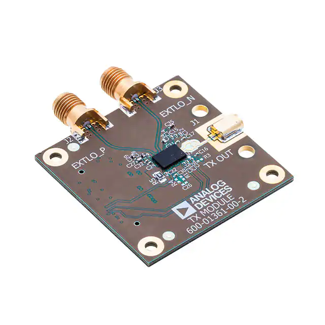
boards (PCBs) that provide on-board crystals, USB interface,
supply regulators, and SMA cables for connectorized I/Q
interfaces. Software is supplied to allow the user to read from
and write to all chip level registers using graphical user interface
(GUI) or to upload previously saved register settings.
14423-019
For more information about the HMC6300 evaluation kit, see
the EK1HMC6350 User Guide. The EK1HMC6350 contains all
that is required to set up a simplex 60 GHz millimeterwave link
using standard RF cable interfaces for baseband input and
output. The kit comes with two motherboard printed circuit
Figure 19. Evaluation PCB Daughter Board
Rev. C | Page 22 of 25
�Data Sheet
HMC6300
3
1
RFOUTN
U1
2
RFOUTP
HMC6300
4MIL-BALUN_60GHz
92_MMPX-S50-0-1/111_NM-1
E1
RFOUTN
D1
RFOUTP
DET_OUT
REF_OUT
DEPOP
C26
1µF
DEPOP
EXTLO_N
R1
1kΩ
C30
1nF
R4
1kΩ
J3
B9
B10
DEPOP
H8
SMA
H9
EXTLO_P
FMP_I
FMM_I
J2
A10
A11
PS_4V_2
PS_4V_2
ANA_RFVGA
ANA_RFVGA
GND
GND
TX_VCC_PA
TX_VCC_RFVGA
TX_VDDD
TX_VCC_TRIP
TX_VCC_TRIP
GND
TX_VCC_VCO
TX_VCC_VCO
GND
TX_VDD_SYN
NC
GND
TX_VCC_DIV
TX_VCC_DIV
TX_VCC_IF
TX_VCC_MIX
TX_VCC_DRV
TX_VCC_DRV
GND
REF_OUT
DECT_OUT
GND
PS_4V_1
PS_4V_1
1
3
5
7
9
11
13
15
17
19
21
23
25
27
29
31
33
35
37
39
41
43
45
47
49
51
53
55
57
59
GROUNDING
J4
QTH-030-01-F-D-A
2
4
6
8
10
12
14
16
18
20
22
24
26
28
30
32
34
36
38
40
42
44
46
48
50
52
54
56
58
60
B2
TX_SCANOUT
G4
RESET
G6
DATA
H3
ENABLE
H4
CLK
H5
ANA_IFVGA
H6
ANA_RFVGA
H2
GND
DATA
ENABLE
CLK
TX_SCANOUT
RESET
GND
GND
GND
BB_QM
BB_QP
GND
TX_REFCLKP D12
BB_IM
BB_IP
TX_REFCLKN E12
GND
GND
GND
GND
C11
TX_REFCLKM
TX_REFCLKP
R5
0
GND
GND
GND
GND
C12
VSS_GND
E11
FMP_I
FMM_I
GND
D11
G8
FMP_Q
FMM_Q
G9
H7
GND
H10
BB_QM
EXTFIL_N
BB_QP
C15
1nF
EXTLO_P
G2
F12
C24
1nF TX_VDDD
G5
DECT_OUT
REF_OUT
A2
A4
A5
BB_QM
BB_QP
FMM_I
FMP_I
BB_IM A6
A7
BB_IP
BB_IM
BB_IP
A8
FMM_Q
FMP_Q
FMM_Q
RFB
FMP_Q
A9
RESET
DATA
VREG_OUT
VCO_RCAP
VCC_MIX
ENABLE
VCC_IF
CLK
REF_CLKP
VCC_DIV
VCC_DIV
VSS_LPF_BIAS_PLL
VCC_PAp
VCC_PAn
VCC_DRV
VCC_DRV
VSS_VCO
VCC_VCO
VSS_VCO
VCC_VCO
GND
GND
GND
VDD_SYN
GND
VDDD
GND
C21
1nF
TX_VCC_TRIP
C23
1nF
TX_VCC_RFVGA
TX_VCC_DIV
A12
B11
C14
1nF
C22
1nF
PS_4V_1
B1
C16
1nF
G1
A3
TX_VCC_DRV
H1
C31
1nF
PS_4V_2
C17
1nF
G10
G11
B5
TX_VCC_VCO
C32
1nF
B6
B7
B8
C1
F1
C12
1nF
Figure 20. Evaluation Daughter Board PCB Schematic
Rev. C | Page 23 of 25
C29
100nF
B4
VSS_VCO
VDD_PA
TX_VCC_IF
C28 100pF
100nF
B3
VCC_DIV B12
VSS_DIV
VSS_REF_DIG
G12
VCC_RFVGA G3
REF_CLKN
VSS_CP_PFD
F11
VCC_TRIP G7
ANA_IFVGA
ANA_RFVGA
TX_VCC_MIX
C20
1nF
C27
SCANOUT
GND
TX_VDD_SYN
RFB
DEPOP
EXTLO_N
VSS_VCO
H11
VSS_VCO
H12
VSS_VCO
TX_VCC_PA
A1
EXTFIL_P
SMA
RFB
R3
1kΩ
14423-020
F1
TX_OUT
J1
�Data Sheet
C48
R70
FMP I
J20
FMP Q
FMM I
FMM Q
C50
TX MODULE
+
C87
+
C93
R82
J32
C68
R86
J28
60
DECT OUT
R184
R183
R182
R181
R180
R179
R178
R177
R176
R175
R174
59
USB-LED
U17
J33
TX IFVGA
C94
C58
R57
R58
R99
R59
C63
R97
R98
C69
R89
R87
R94
R85
+ C88
U15
R95 R90
C66
C70
R71
+
R56
U18
2
C49
R88
C95
C67
R93
R91
R92
R73
C89
U16
R96
FB6
1
2
J26
1
R72
TX RFVGA
C65
2
C52
J27
C64
C47
C44
R61
U3
C43
J19
C11
BB IP
J18
C10
C9
C8
BB IM
J17
1
J1
D4
C6
C7
BB QP
R66
R68
BB QM
J13
R119
C46
C42 R60
R63
R65
R64
R62
USB
C51
Y1
C45
U11 R67 R69
J14
C5
J16
J15
C12
HMC6300
REF OUT
J34
PWR-SUPPLY-LED
R192
MUX
SEL0
J11
Figure 21. Evaluation PCB Motherboard
Rev. C | Page 24 of 25
J12
60
59
1
VOUT IP
VOUT IM
C1
VOUT QP
C2
VOUT QM
C3
R163 C83
C4
R159 R158
2
+
+
C91
R157
MUX
SEL1
C85
+
J21
R161 C81
R162 C82
R156
C25
C24
J29
J30
J10
J9
14423-021
EXT CLOCK
U22
D8 R129
R14
R13
R23
R155
R152
U19
R22
R21
R160 C80
C79
R153
R154
FB1
FB4
D7 R128
C13
C26
Y3
R130
C21
R24
FB2
R20
R19
C14
R18
R16
R15 R17
Y4
R131
C92
J31
RX IFVGA
R173
R172
R171
R170
R169
R168
R167
R166
R165
R164
C84
C90
R187
R186
RX LNA CTL
C86
C109
C108
C105
RX MODULE
600-01205-00-2
C100
C99
R195
C103
5V SUPPLY
R77
C107 U26
U27
R123
C102
U25 R194
C110
60 GHz EVALUATION BOARD
R103
R185
R189
R188
+
C104
J8
R193
C101
U24
R79
R190
C106
C56
C96
C97
R191
U23
C28
D1 R32
C98
�Data Sheet
HMC6300
OUTLINE DIMENSIONS
6.050
6.000
5.950
12
11
10
9
8
7
6
5
4
3
2
1
A
B
BALL A1
IDENTIFIER
1.258
4.050
4.000
3.950
1.03
C
0.858
0.406
0.425
3.50
REF
0.455
0.075
D
E
1.115
0.50
BSC
F
G
H
TOP VIEW
0.25
BSC
(BALL SIDE DOWN)
SIDE VIEW
SEATING
PLANE
0.220
0.190
0.160
0.310
0.270
0.230
PKG-005029
0.595
0.565
0.535
COPLANARITY
0.10
01-25-2016-A
0.815
0.755
0.695
BOTTOM VIEW
0.50 BSC(BALL SIDE UP)
GROUND AREA
0.25 BSC
5.50 REF
5.75 REF
Figure 22. 65-Ball Wafer Level Ball Grid Array [WLBGA]
(BF-65-1)
Dimensions shown in millimeters
ORDERING GUIDE
Model
HMC6300BG46
Temperature Range
−40°C to +85°C
MSL Rating 1
MSL1
EV1HMC6300BG46
EK1HMC6350
Package Description
65-Ball Wafer Level Ball Grid Array [WLBGA]
Package Option
BF-65-1
Branding 2
BBFZ
#YYWW
XXXXXXXX-XX
Evaluation Board, PCB Only
60 GHz SMT Transceiver Evaluation Kit
Maximum peak reflow temperature of 260°C. The peak reflow temperature must not exceed the maximum temperature for which the package is qualified according
to the moisture sensitivity level (MSL1).
2
BBFZ = RoHS Compliant Part, #YYWW indicates the year and week number, and the assembly lot number is indicated by XXXXXXXX-XX.
1
©2016–2017 Analog Devices, Inc. All rights reserved. Trademarks and
registered trademarks are the property of their respective owners.
D14423-0-6/17(C)
Rev. C | Page 25 of 25
�