FEATURES
FUNCTIONAL BLOCK DIAGRAM
Gain: 14 dB typical
Operational frequency range: 0.01 GHz to 10 GHz
Input/output internally matched to 50 Ω
High input linearity
1 dB compression (P1dB): 20 dBm typical
Output third-order intercept (OIP3): 33 dBm typical
Supply voltage: 5 V typical
2 mm × 2 mm, 6-lead lead frame chip scale package
HMC788A
6 NIC
NIC 1
RFIN 2
5 RFOUT
4 NIC
GND 3
PACKAGE
BASE
16204-001
Data Sheet
0.01 GHz to 10 GHz, MMIC, GaAs, pHEMT
RF Gain Block
HMC788A
Figure 1.
APPLICATIONS
Cellular, 3G, LTE, WiMAX, and 4G
LO driver applications
Microwave radio
Test and measurement equipment
Ultra wideband (UWB) communications
GENERAL DESCRIPTION
The HMC788A is a 0.01 GHz to 10 GHz, gain block, monolithic
microwave integrated circuit (MMIC) amplifier using gallium
arsenide (GaAs), pseudomorphic high electron mobility transistor
(pHEMT) technology.
This 2 mm × 2 mm LFCSP amplifier can be used as either a
cascadable 50 Ω gain stage, or to drive the local oscillator (LO) port
of many of the single and double balanced mixers from Analog
Devices, Inc. with up to 20 dBm output power.
Rev. D
The HMC788A offers 14 dB of gain and an output IP3 of
33 dBm while requiring only 76 mA from a 5 V supply.
The Darlington feedback pair exhibits reduced sensitivity to
normal process variations and yields excellent gain stability
over temperature while requiring a minimal number of external
bias components.
Document Feedback
Information furnished by Analog Devices is believed to be accurate and reliable. However, no
responsibility is assumed by Analog Devices for its use, nor for any infringements of patents or other
rights of third parties that may result from its use. Specifications subject to change without notice. No
license is granted by implication or otherwise under any patent or patent rights of Analog Devices.
Trademarks and registered trademarks are the property of their respective owners.
One Technology Way, P.O. Box 9106, Norwood, MA 02062-9106, U.S.A.
Tel: 781.329.4700
©2019 Analog Devices, Inc. All rights reserved.
Technical Support
www.analog.com
�HMC788A
Data Sheet
TABLE OF CONTENTS
Features .............................................................................................. 1
Pin Configuration and Function Descriptions..............................5
Applications ....................................................................................... 1
Interface Schematics .....................................................................5
Functional Block Diagram .............................................................. 1
Typical Performance Characteristics ..............................................6
General Description ......................................................................... 1
Theory of Operation .........................................................................9
Revision History ............................................................................... 2
Basic Connections .........................................................................9
Specifications..................................................................................... 3
Applications Information .............................................................. 10
Electrical Specifications ............................................................... 3
Evaluation PCB ........................................................................... 10
Absolute Maximum Ratings ............................................................ 4
Outline Dimensions ....................................................................... 12
Thermal Resistance ...................................................................... 4
Ordering Guide .......................................................................... 12
ESD Caution .................................................................................. 4
REVISION HISTORY
6/2019—Rev. C to Rev. D
Changes to Table 5 .......................................................................... 10
Changes to Ordering Guide .......................................................... 12
9/2018—Rev. B to Rev. C
Change to RF Input Power (RFIN), VCC = 5 V Parameter,
Table 2 ................................................................................................ 4
11/2017—Rev. A to Rev. B
Changes to Continuous Power Dissipation, PDISS Parameter and
Junction (TJ) Temperature Parameter, Table 2 ............................. 4
This Hittite Microwave Products data sheet has been reformatted to
meet the styles and standards of Analog Devices, Inc.
10/2017—v00.0913 to Rev. A
Changes to Product Title, Features Section, General Description
Section, and Figure 1 .........................................................................1
Changes to Table 1.............................................................................3
Changes to Table 2.............................................................................4
Added Thermal Resistance Section and Table 3; Renumbered
Sequentially ........................................................................................4
Changes to Figure 2, Table 4, and Figure 3 ....................................5
Changes to Typical Perfomance Characteristics Section .............6
Added Figure 17; Renumbered Sequentially .................................8
Added Theory of Operation Section ..............................................9
Added Applications Information Section Heading ................... 10
Changes to Evaluation PCB Section and Figure 18 ................... 10
Updated Outline Dimensions ....................................................... 12
Changes to Ordering Guide .......................................................... 12
Rev. D | Page 2 of 12
�Data Sheet
HMC788A
SPECIFICATIONS
ELECTRICAL SPECIFICATIONS
Collector bias voltage (VCC) = 5 V, TCASE = 25°C, 6.35 µH external inductor between VCC and RFOUT, 50 Ω system, unless otherwise noted.
Table 1.
Parameter
OVERALL FUNCTION
Frequency Range
Gain
Symbol
Min
0.01
12
9
Gain Variation Over Temperature
Reverse Isolation
RADIO FREQUENCY (RF) INPUT INTERFACE
Input Return Loss
RF OUTPUT INTERFACE
Output Power for 1 dB Compression
P1dB
18
15
Output Return Loss
DISTORTION AND NOISE
Output Third-Order Intercept
Noise Figure
POWER INTERFACE
Supply Voltage
Supply Current
OIP3
NF
ICC
4.5
60
Typ
Max
Unit
Test Conditions/Comments
10
14
12
0.004
0.007
23
20
GHz
dB
dB
dB/°C
dB/°C
dB
dB
0.01 GHz to 6.0 GHz
6.0 GHz to 10.0 GHz
0.01 GHz to 6.0 GHz
6.0 GHz to 10.0 GHz
0.01 GHz to 6.0 GHz
6.0 GHz to 10 GHz
16
9
dB
dB
0.01 GHz to 6.0 GHz
6.0 GHz to 10.0 GHz
20
18
9
12
dBm
dBm
dB
dB
0.01 GHz to 6.0 GHz
6.0 GHz to 10.0 GHz
0.01 GHz to 6.0 GHz
6.0 GHz to 10.0 GHz
33
30
6
7
dBm
dBm
dB
dB
0.01 GHz to 6.0 GHz
6.0 GHz to 10.0 GHz
0.01 GHz to 6.0 GHz
6.0 GHz to 10.0 GHz
V
mA
mA
mA
VCC = 4.5 V
VCC = 5 V
VCC = 5.5 V
5
65
76
87
Rev. D | Page 3 of 12
5.5
90
�HMC788A
Data Sheet
ABSOLUTE MAXIMUM RATINGS
THERMAL RESISTANCE
Table 2.
Parameter
Collector Bias Voltage (VCC)
RF Input Power (RFIN), VCC = 5 V
Continuous Power Dissipation, PDISS
(TCASE = 85°C, Derate 8.5 mW/°C Above 85°C)
Junction (TJ) Temperature
Operating (TOPR) Temperature Range
Storage Temperature Range
Electrostatic Discharge (ESD) Sensitivity,
Human Body Model (HBM)
Thermal performance is directly linked to printed circuit board
(PCB) design and operating environment. Careful attention to
PCB thermal design is required.
Rating
7V
20 dBm
0.76 W
175°C
−40°C to +85°C
−65°C to +150°C
Class 1A
Stresses at or above those listed under Absolute Maximum
Ratings may cause permanent damage to the product. This is a
stress rating only; functional operation of the product at these
or any other conditions above those indicated in the operational
section of this specification is not implied. Operation beyond
the maximum operating conditions for extended periods may
affect product reliability.
θJC is the junction to case thermal resistance.
Table 3. Thermal Resistance
Package Type
CP-6-101
1
θJC
118.0
Unit
°C/W
Thermal impedance simulated values are based on a JEDEC 2S2P thermal
test board with nine thermal vias. See JEDEC JESD51.
ESD CAUTION
Rev. D | Page 4 of 12
�Data Sheet
HMC788A
PIN CONFIGURATION AND FUNCTION DESCRIPTIONS
6 NIC
NIC 1
HMC788A
RFIN 2
GND 3
TOP VIEW
5 RFOUT
(Not to Scale)
4 NIC
NOTES
1. NIC = NOT INTERNALLY CONNECTED.
THE PINS ARE NOT CONNECTED
INTERNALLY; HOWEVER, ALL DATA
SHOWN HEREIN WAS MEASURED
WITH THESE PINS CONNECTED TO
GROUND EXTERNALLY.
2. EXPOSED PAD. THE EXPOSED PAD
MUST BE CONNECTED TO GROUND
FOR PROPER OPERATION.
16204-002
PACKAGE
BASE
Figure 2. Pin Configuration
Table 4. Pin Function Descriptions
Pin No.
1, 4, 6
Mnemonic
NIC
2
3
5
RFIN
GND
RFOUT
EPAD
Description
Not Internally Connected. The pins are not connected internally; however, all data shown herein was measured
with these pins connected to GND externally.
RF Input. This pin is dc-coupled and ac matched to 50 Ω. An external dc blocking capacitor is required on this pin.
Ground. This pin must be connected to ground.
RF Output. This pin is ac matched to 50 Ω and supplies dc bias for the output stage.
Exposed Pad. The exposed pad must be connected to GND for proper operation.
GND
RFOUT
16204-003
RFIN
16204-004
INTERFACE SCHEMATICS
Figure 4. GND Interface Schematic
Figure 3. RFIN, RFOUT Interface Schematic
Rev. D | Page 5 of 12
�HMC788A
Data Sheet
TYPICAL PERFORMANCE CHARACTERISTICS
20
20
10
GAIN (dB)
15
0
–10
10
S22
S21
S11
–30
0
2
4
6
8
10
12
14
16
FREQUENCY (GHz)
5
0
–5
OUTPUT RETURN LOSS (dB)
–5
+85°C
+25°C
–40°C
–25
–30
0
2
4
6
8
10
12
FREQUENCY (GHz)
10
12
–15
–20
+85°C
+25°C
–40°C
–30
0
2
4
6
8
10
12
FREQUENCY (GHz)
Figure 6. Input Return Loss vs. Frequency at Various Temperatures
Figure 9. Output Return Loss vs. Frequency at Various Temperatures
–10
20
+85°C
+25°C
–40°C
–12
–14
15
NOISE FIGURE (dB)
–16
–18
–20
–22
–24
10
5
–26
–28
–30
0
2
4
6
8
10
12
FREQUENCY (GHz)
0
0
2
4
6
8
10
12
FREQUENCY (GHz)
Figure 7. Reverse Isolation vs. Frequency at Various Temperatures
Figure 10. Noise Figure vs. Frequency at Various Temperatures
Rev. D | Page 6 of 12
16204-010
+85°C
+25°C
–40°C
16204-007
REVERSE ISOLATION (dB)
8
–10
–25
16204-006
INPUT RETURN LOSS (dB)
0
–20
6
Figure 8. Gain vs. Frequency at Various Temperatures
0
–15
4
FREQUENCY (GHz)
Figure 5. Gain, Input Return Loss, and Output Return Loss vs. Frequency;
S21 is Gain, S11 is Input Return Loss, S22 is Output Return Loss
–10
2
16204-008
+85°C
+25°C
–40°C
16204-009
–20
16204-005
GAIN, INPUT RETURN LOSS, AND
OUTPUT RETURN LOSS
30
�Data Sheet
HMC788A
25
45
40
20
OUTPUT IP3 (dBm)
P1dB (dBm)
35
15
10
30
25
20
5
6
10
8
12
FREQUENCY (GHz)
10
0
8
10
12
25
PAE
GAIN (dBm)
POUT (dBm)
20
45
40
PSAT (dBm)
35
30
25
15
10
20
15
5
10
+85°C
+25°C
–40°C
5
–5
0
INPUT POWER (dBm)
5
10
0
16204-012
0
–10
0
2
4
6
FREQUENCY (GHz)
Figure 12. Output Power (POUT), Gain, and Power Added Efficiency (PAE)
vs. Input Power at 1 GHz
8
10
12
16204-014
POUT (dBm), GAIN (dB), AND PAE (%)
6
Figure 13. Output IP3 vs. Frequency at Various Temperatures;
5 dBm per Tone Output Power
60
50
4
FREQUENCY (GHz)
Figure 11. P1dB vs. Frequency at Various Temperatures
55
2
16204-013
4
2
16204-011
0
0
+85°C
+25°C
–40°C
15
+85°C
+25°C
–40°C
Figure 14. Saturation Power (PSAT) vs. Frequency at Various Temperatures
Rev. D | Page 7 of 12
�HMC788A
Data Sheet
–80
PAE
GAIN (dBm)
POUT (dBm)
25
–90
ADDITIVE PHASE NOISE (dBc/Hz)
POUT (dBm), GAIN (dB), AND PAE (%)
30
20
15
10
5
–100
–110
–120
–130
–140
–150
–160
0
2
4
6
8
10
12
INPUT POWER (dBm)
–180
100
16204-015
0
30
IP3
P1dB
GAIN
20
5.5
SUPPLY VOLTAGE (V)
16204-016
GAIN (dB), P1dB (dBm), AND IP3 (dBm)
100k
Figure 17. Additive Phase Noise vs. Offset Frequency;
RF Frequency = 5 GHz, RF Input Power = 6 dBm (P1dB)
40
5.0
10k
OFFSET FREQUENCY (Hz)
Figure 15. POUT, Gain, and PAE vs. Input Power at 10 GHz
10
4.5
1k
Figure 16. Gain, P1dB, and IP3 vs. Supply Voltage at 1 GHz
Rev. D | Page 8 of 12
1M
16204-017
–170
�Data Sheet
HMC788A
THEORY OF OPERATION
The HMC788A is designed with a Darlington feedback pair that
exhibits reduced sensitivity to normal process variations and yields
excellent gain stability over temperature while requiring minimal
external bias components. The amplifier can be operated from a
5 V supply by adding a choke inductor from the amplifier
output to VCC.
BASIC CONNECTIONS
The HMC788A RF gain block is a fixed gain amplifier with singleended input and output ports featuring impedances nominally
equal to 50 Ω over the 0.01 GHz to 10 GHz frequency range. The
input and output impedances are sufficiently stable across
variations in temperature and supply voltage such that the
HMC788A can be directly inserted into a 50 Ω system with no
impedance matching circuitry required.
The input pin, RFIN, is dc-coupled and ac matched to 50 Ω. A dc
blocking capacitor must be connected between the source that
drives the HMC788A and the RFIN pin.
It is critical to supply very low inductance ground connections
to the GND pin as well as to the backside exposed pad, ensuring
stable operation. It is recommended that the NIC pins also be
connected to GND.
The HMC788A is designed to operate with a supply voltage of
5 V, which is connected through an external RF choke between
the supply voltage and the output pin, RFOUT. The inductance of
the RF choke must be approximately 6 µH, and care must be
taken to ensure that the lowest series self resonant frequency of
this choke is well above the maximum frequency of operation
for the HMC788A. Consequently, a dc blocking capacitor must
be connected between the bias connection to RFOUT and the
output load. The value of this capacitor is not critical, but it is
recommended to be 100 pF or larger.
Bypass the bias supply voltage, VCC, using a large value capacitance
(approximately 2.2 µF or larger) and a smaller, high frequency
bypass capacitor (approximately 100 pF).
The recommended connections and components are shown in
the Evaluation PCB section.
Rev. D | Page 9 of 12
�HMC788A
Data Sheet
APPLICATIONS INFORMATION
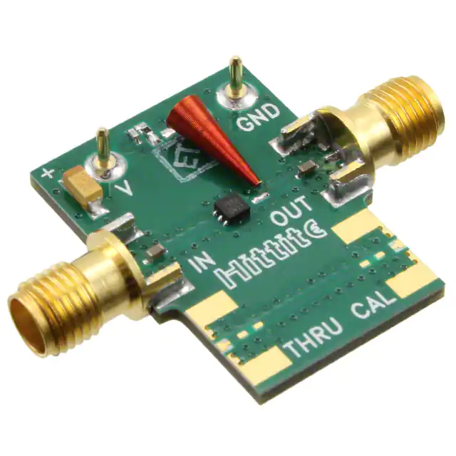
EVALUATION PCB
The PCB used in this application must use RF circuit design
techniques. Signal lines must have 50 Ω impedance while the
package ground leads and exposed pad must be connected
directly to the ground plane similar to that shown in Figure 19.
A sufficient number of via holes must be used to connect the top
and bottom ground planes. The EV1HMC788ALP2 evaluation
board must be mounted to an appropriate heat sink.
Figure 18 shows the schematic of the EV1HMC788ALP2
evaluation board. The board is powered by a single supply between
4.5 V and 5.5 V and is decoupled by a 2.2 µF capacitor and a
100 pF capacitor. DC blocking capacitors are installed at the RFIN
and RFOUT ports. Note that inductor L1 is a required component to
apply the VCC = 5 V bias to the RFOUT pin.
Table 5. List of Materials for the Evaluation PCB
EV1HMC788ALP21
Item
J1 to J2
J5, J6
C1, C2
C3
C4
R1
L1
U1
PCB2
1
2
Reference this number when ordering the complete evaluation PCB.
The circuit board material is Rogers 4350.
VCC
C4
2.2µF
C3
100pF
L1
6.35µH
C1
.01µF
C2
.01µF
RFIN
RFOUT
PIN 3
PIN 5
PACKAGE BOTTOM
MUST BE CONNECTED
TO RF GROUND.
16204-018
PIN 2
Description
PCB mount Subminiature Version A (SMA) connector
DC pin
0.01 μF capacitor, 0502 package
100 pF capacitor, 0402 package
2.2 μF Case A package
0 Ω resistor, 0402 package
Inductor, conical 6.35 μH, P/N CC75T38K240G5
(Piconics)
HMC788ALP2E
129549 evaluation PCB
Figure 18. Evaluation Board Schematic
Rev. D | Page 10 of 12
�HMC788A
16204-019
Data Sheet
Figure 19. Evaluation Board, Top View
Rev. D | Page 11 of 12
�HMC788A
Data Sheet
OUTLINE DIMENSIONS
1.50
1.40
1.30
8
5
PIN 1 INDEX
AREA
PKG-004900/005352
SEATING
PLANE
0.90
0.80
0.70
EXPOSED
PAD
TOP VIEW
0.90
0.85
0.80
DETAIL A
(JEDEC 95)
0.65
BSC
SIDE VIEW
0.30
0.25
0.20
0.40
0.35
0.30
4
0.05 MAX
0.02 NOM
COPLANARITY
0.08
1
PIN 1
IN D IC ATO R AR E A OP T I O N S
(SEE DETAIL A)
BOTTOM VIEW
1.30 REF
FOR PROPER CONNECTION OF
THE EXPOSED PAD, REFER TO
THE PIN CONFIGURATION AND
FUNCTION DESCRIPTIONS
SECTION OF THIS DATA SHEET.
0.203 REF
08-17-2018-C
2.05
2.00 SQ
1.95
Figure 20. 6-Lead Lead Frame Chip Scale Package [LFCSP]
2 mm × 2 mm Body and 0.85 mm Package Height
(CP-6-10)
Dimensions shown in millimeters
ORDERING GUIDE
Model1
HMC788ALP2E
HMC788ALP2ETR
EV1HMC788ALP2
1
2
Temperature
Range
−40°C to +85°C
−40°C to +85°C
MSL
Rating2
MSL3
MSL3
Package Description
6-Lead Lead Frame Chip Scale Package [LFCSP]
6-Lead Lead Frame Chip Scale Package [LFCSP]
Evaluation Board
All models are RoHS Compliant.
See the Absolute Maximum Ratings section.
©2019 Analog Devices, Inc. All rights reserved. Trademarks and
registered trademarks are the property of their respective owners.
D16204-0-6/19(D)
Rev. D | Page 12 of 12
Package
Option
CP-6-10
CP-6-10
Marking
Code
Y7H
Y7H
�