0.1 GHz to 6.0 GHz, 0.5 dB LSB, 6-Bit,
Silicon Digital Attenuator
HMC1122
Data Sheet
LE
4
GND
5
ATTIN
6
D2
D3
D4
D5
19
SERIAL/
PARALLEL
INTERFACE
6-BIT/
DIGITAL
ATTENUATOR
GND
7
8
9
10
11
18
VDD
17
PUP1
16
PUP2
15
SEROUT
14
GND
13
ATTOUT
12
PACKAGE
BASE
GND
13719-001
3
20
GND
SERIN
21
GND
2
22
GND
CLK
23
GND
1
24
GND
P/S
D1
FUNCTIONAL BLOCK DIAGRAM
Attenuation range: 0.5 dB LSB steps to 31.5 dB
Low insertion loss
1.1 dB at 1 GHz
1.3 dB at 2 GHz
Typical step error: less than ±0.1 dB
Excellent attenuation accuracy
Safe state transitions
High linearity
Input 0.1dB compression (P0.1dB): 30 dBm typical
Input third-order intercept (IP3): 55 dBm typical
RF settling time (0.05 dB final RF output): 250 ns
Low phase shift error: 6° at 1 GHz
Single supply operation: 3.3 V to 5 V
ESD rating: Class 2 (2 kV HBM)
24-lead, 4 mm × 4 mm LFCSP package: 16 mm2
Pin compatible to the HMC624A
D0
FEATURES
Figure 1.
APPLICATIONS
Cellular infrastructure
Microwave radios and very small aperture terminals (VSATs)
Test equipment and sensors
IF and RF designs
GENERAL DESCRIPTION
The HMC1122 is a 6-bit digital attenuator operating from
0.1 GHz to 6 GHz with a 31.5 dB attenuation control range in
0.5 dB steps.
The HMC1122 is implemented in a silicon process, offering
very fast settling time, low power consumption, and high ESD
robustness. The device features safe state transitions and
optimized for excellent step accuracy and high linearity over
frequency and temperature range. The RF input and output are
internally matched to 50 Ω and do not require any external
matching components. The design is bidirectional; therefore,
the RF input and output are interchangeable.
Rev. B
The HMC1122 operates on a single supply ranging from 3.3 V
to 5 V with no performance change due to an on-chip regulator.
The device incorporates a driver that provides both serial and
parallel control of the attenuator. The device also features a userselectable power-up state and a serial output port for cascading
other serial controlled components.
The HMC1122 comes in a RoHS compliant, compact, 4 mm ×
4 mm LFCSP package, and is pin compatible to the HMC624A.
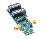
A fully populated evaluation board is available.
Document Feedback
Information furnished by Analog Devices is believed to be accurate and reliable. However, no
responsibility is assumed by Analog Devices for its use, nor for any infringements of patents or other
rights of third parties that may result from its use. Specifications subject to change without notice. No
license is granted by implication or otherwise under any patent or patent rights of Analog Devices.
Trademarks and registered trademarks are the property of their respective owners.
One Technology Way, P.O. Box 9106, Norwood, MA 02062-9106, U.S.A.
Tel: 781.329.4700 ©2016–2017 Analog Devices, Inc. All rights reserved.
Technical Support
www.analog.com
�HMC1122
Data Sheet
TABLE OF CONTENTS
Features .............................................................................................. 1
Input Power Compression and Third-Order Intercept ............9
Applications ....................................................................................... 1
Theory of Operation ...................................................................... 10
Functional Block Diagram .............................................................. 1
Power Supply............................................................................... 10
General Description ......................................................................... 1
RF Input and Output ................................................................. 10
Revision History ............................................................................... 2
Serial or Parallel Mode Selection ............................................. 10
Specifications..................................................................................... 3
Serial Mode Interface ................................................................. 10
Timing Specifications .................................................................. 4
Parallel Mode Interface.............................................................. 11
Absolute Maximum Ratings............................................................ 5
Power-Up Interface .................................................................... 11
ESD Caution .................................................................................. 5
Applications Information .............................................................. 12
Pin Configuration and Function Descriptions ............................. 6
Evaluation Printed Circuit Board ............................................ 12
Interface Schematics..................................................................... 6
Evaluation Board Schematic and Artwork ............................. 13
Typical Performance Characteristics ............................................. 7
Outline Dimensions ....................................................................... 15
Insertion Loss, Return Loss, State Error, Step Error, and
Relative Phase................................................................................ 7
Ordering Guide .......................................................................... 15
REVISION HISTORY
9/2017—Rev. A to Rev. B
Changed CP-24-16 to HCP-24-3 ................................. Throughout
Updated Outline Dimensions ....................................................... 15
Changes to Ordering Guide .......................................................... 15
8/2017—Rev. 0 to Rev. A
Added Timing Specifications Section ............................................ 4
Moved Table 2 ................................................................................... 4
Change to Figure 5 ........................................................................... 6
Changes to Figure 26 ...................................................................... 11
Updated Outline Dimensions ....................................................... 15
4/2016—Revision 0: Initial Version
Rev. B | Page 2 of 15
�Data Sheet
HMC1122
SPECIFICATIONS
VDD = 3.3 V to 5 V, TA = 25°C, 50 Ω system, unless otherwise noted.
Table 1.
Parameter
FREQUENCY RANGE
INSERTION LOSS
Symbol
At 0.2 GHz to 1.0 GHz
At 1.0 GHz to 2.0 GHz
At 2.0 GHz to 4.0 GHz
At 4.0 GHz to 6.0 GHz
At 0.2 GHz to 6 GHz
Between minimum and maximum
attenuation states
Between any successive
attenuation states
Between any successive
attenuation states
All attenuation states; referenced
to insertion loss state
ATTENUATION
Range
Step Size
Step Error
Accuracy
Overshoot
RETURN LOSS
(ATTIN and ATTOUT)
RELATIVE PHASE
SWITCHING CHARACTERISTICS
Rise and Fall Time
On and Off Time
0.1 dB Settling Time
tRISE, tFALL
tON, tOFF
0.05 dB Settling Time
INPUT LINEARITY
Input 0.1 dB Compression
Input Third-Order Intercept
SUPPLY CURRENT
Test Conditions/Comments
P0.1dB
IP3
IDD
Between all attenuation states
At 1.0 GHz, minimum attenuation
(worst case)
At 2.0 GHz, minimum attenuation
(worst case)
At 4.0 GHz, minimum attenuation
(worst case)
At 6.0 GHz, maximum attenuation
(worst case)
Between minimum and maximum
attenuation states
At 1.0 GHz
At 2.0 GHz
At 4.0 GHz
At 6.0 GHz
Between all attenuation states
10% to 90% of RF output
50% VCTL to 90% of RF output
50% VCTL to 0.1 dB of final RF
output
50% VCTL to 0.05 dB of final RF
output
All attenuation states, 0.2 GHz to
6 GHz
Two-tone input power = 15 dBm
each tone, Δf = 1 MHz
VDD = 3.3 V
VDD = 5.0 V
Rev. B | Page 3 of 15
Min
0.1
Typ
1.1
1.3
1.7
2.0
Max
6.0
1.8
2.0
2.4
2.8
Unit
GHz
dB
dB
dB
dB
31.5
dB
0.5
dB
很抱歉,暂时无法提供与“EV2HMC1122LP4M”相匹配的价格&库存,您可以联系我们找货
免费人工找货- 国内价格
- 1+2181.76200
- 200+2049.10560