EV1HMC6832ALP5L/EV2HMC6832ALP5L User Guide
UG-942
One Technology Way • P.O. Box 9106 • Norwood, MA 02062-9106, U.S.A. • Tel: 781.329.4700 • Fax: 781.461.3113 • www.analog.com
Evaluation Boards for the HMC6832
3.5 GHz, Low Noise, 2:8 Differential Fanout Buffer
FEATURES
GENERAL DESCRIPTION
On-board LDO voltage regulator for 2.5 V/3.3 V device under
test (DUT) supply
LDO can be bypassed to allow for an external supply
AC-coupled differential SMA connectors
SMA connectors for
2 differential input clocks
8 analog differential outputs
Jumpers to enable/disable the LDO voltage regulator
Clip on access points for power/ground
Jumper for input clock selection
Matched RF differential traces
This user guide describes the two evaluation boards for
evaluating the HMC6832 fully differential output buffer.
Both evaluation boards, EV1HMC6832ALP5L and
EV2HMC6832ALP5L, allow access to all HMC6832
input/outputs via SMAs.
The EV1HMC6832ALP5L is configured for the LVPECL
version of the product whereas the EV2HMC6832ALP5L is
configured for LVDS. Each board has an on-board low dropout
(LDO) regulator for 2.5 V/3.3 V operation that can be disabled
to use an external supply. Each board has matched RF
differential traces for testing output to output channel skew.
For full specifications on the HMC6832, see the product data
sheet, which should be consulted in conjunction with this user
guide when working with the evaluation board. The evaluation
board schematics and the HMC6832 data sheet are available on
the HMC6832 product page.
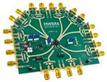
14294-001
PHOTOGRAPH OF EV1HMC6832ALP5L
Figure 1. EV1HMC6832ALP5L Evaluation Board
PLEASE SEE THE LAST PAGE FOR AN IMPORTANT
WARNING AND LEGAL TERMS AND CONDITIONS.
Rev. 0 | Page 1 of 6
�UG-942
EV1HMC6832ALP5L/EV2HMC6832ALP5L User Guide
TABLE OF CONTENTS
Features .............................................................................................. 1
Setting Up Signal Connections ....................................................3
General Description ......................................................................... 1
Bypassing the 5 V LDO Voltage Regulator ................................3
Photograph of EV1HMC6832ALP5L ............................................ 1
Jumper Configurations .....................................................................4
Revision History ............................................................................... 2
Test Equipment Configurations ......................................................5
Getting Started .................................................................................. 3
Powering the Evaluation Board .................................................. 3
REVISION HISTORY
3/16—Revision 0: Initial Version
Rev. 0 | Page 2 of 6
�EV1HMC6832ALP5L/EV2HMC6832ALP5L User Guide
UG-942
GETTING STARTED
SETTING UP SIGNAL CONNECTIONS
For convenience, many of the jumpers are preinstalled on
the evaluation boards as listed in Table 1. The jumper
installation is dependent on the version of the evaluation
board, EV1HMC6832ALP5L or EV2HMC6832ALP5L. Prior
to powering on the evaluation board, it is important to verify
the jumper configuration against Table 1 and Figure 3 for the
physical locations of the jumpers and test points.
There are two ac-coupled inputs to choose from, Input 0 or
Input 1, via the IN_SEL pin of the HMC6832. The input is
determined by J3 on the evaluation board. A signal generator
can be connected to either or both of these inputs and the user
can select between them as follows:
POWERING THE EVALUATION BOARD
•
•
It is important to decide whether to use the on-board voltage
regulator or an external power supply because the jumper
configurations vary accordingly. Refer to Table 1 for the
required jumper configurations.
Connect the output(s) of interest to either an oscilloscope
or a spectrum analyzer for observation and evaluation (see
Figure 4).
BYPASSING THE 5 V LDO VOLTAGE REGULATOR
If using the on-board regulator, apply 5 V to TP3 and ground
either TP1 or TP4. Figure 4 provides an example of this scheme.
In this scenario, install J8 but do not install J7. J6 determines the
output voltage of the regulator and installing J9 allows observation
of the regulator output voltage at TP2. Refer to Table 1 for
additional information about J6 and J9.
VDD
50kΩ
To select Input 0, tie J3 to ground.
To select Input 1, tie J3 to VDD.
To use an external power supply, such as for current measurements, bypass the on-board voltage regulator. To bypass the
regulator, reconfigure the jumpers by installing J7 and not
installing J8. An external supply of either 2.5 V (LVDS or
LVPECL) or 3.3 V (LVPECL only) can then be supplied to TP2
(see Table 2).
IN_SEL
HIGH: IN1
LOW: IN0
OUTP7
INP1
50kΩ
OUTN7
100pF
LVDS
OUTP6
VDD
OUTN6
100pF
50kΩ
INN1
OUTN5
50kΩ
4mA
4mA
4mA
LVDS
OUTP4
OUTN4
4mA
LVDS
OUTP5
4mA
4mA
LVDS
4mA
4mA
OUTP3
VDD
OUTN3
50kΩ
INP0
50kΩ
OUTP2
OUTN2
100pF
OUTN1
100pF
OUTN0
50kΩ
4mA
4mA
4mA
LVDS
OUTP0
50kΩ
INN0
4mA
LVDS
OUTP1
VDD
LVDS
4mA
4mA
LVDS
4mA
4mA
VAC_REF
VDD
100kΩ
CONFIGURATION
CONTROL
LVDS
2mA
LVPECL
Figure 2. Functional Block Diagram
Rev. 0 | Page 3 of 6
14294-002
CONFIG
HIGH: LVDS
LOW: LVPECL
�UG-942
EV1HMC6832ALP5L/EV2HMC6832ALP5L User Guide
JUMPER CONFIGURATIONS
Refer to Figure 3 for jumper and test point locations on the board.
Table 1. Jumper Settings
Jumper
Number
J3
Installed
As needed, depending on input
desired.
J5
Function
Input level for IN_SEL pin. GND
selects Input0 and DUT_VCC selects
Input1.
Determines LVPECL/LVDS mode.
J6
Determines the regulator supply.
Regulator supplies 2.5 V, assuming
it is enabled (J7 not installed) and 5
V is supplied to TP3.
J7
Enables or disables the regulator
output.
Connects or disconnects the
regulator output to the HMC6832
device.
Determines the function of TP2 to
observe the regulator output or to
apply power to the HMC6832
device, depending on the
installation status of J8.
Analog Devices, Inc., use only.
Disables regulator output.
J8
J9
J30
Sets CONFIG pin to proper
configuration mode (LVPECL/LVDS).
Connects the regulator output to
the device.
When J8 is installed, the regulator
output can be observed at TP2.
When J8 is not installed, power can
be applied (2.5 V or 3.3 V) via TP2.
Do not install.
Uninstalled
If not installed, default is
Input0 as IN_SEL has an
internal pull-down
Sets HMC6832 to LVDS
mode due to internal
pull-up on the device.
Regulator supplies 3.3 V,
assuming it is enabled (J7
not installed) and 5 V is
supplied to TP3.
Enables regulator output.
Preinstalled on
Evaluation
Board
No
Yes
Yes
No
Disconnects the
regulator output and the
device.
Power cannot be applied
or observed at TP2.
Yes
Analog Devices use only.
No
Yes
Table 2. Test Points
Test Point
Number
TP1
TP2
TP3
TP4
Function
Ground connection.
When J8 and J9 are installed, TP2 observes the regulator output. When J9 is installed and J8 is not installed, TP2
supplies power (2.5 V or 3.3 V) to the HMC6832.
5 V supply for the on-board regulator.
Ground connection.
Rev. 0 | Page 4 of 6
�EV1HMC6832ALP5L/EV2HMC6832ALP5L User Guide
UG-942
TEST EQUIPMENT CONFIGURATIONS
The test equipment requirements and setup configurations are shown in Figure 3 and Figure 4.
J9
J8
TP2
J5
J6
TP3
J7
J30
J3
TP1
14294-004
TP4
OUTP6
+5V
OUTP7
DC POWER SUPPLY
OUTN6
OUTN7
Figure 3. Test Point and Jumper Labels on EV1HMC6832ALP5L/EV2HMC6832ALP5L
GND
O
TP1
OSCILLOSCOPE/
SIGNAL ANALYZER
TP3
INP1
CLOCK SOURCE/
SIGNAL GENERATOR
N5
UT
P5
UT
O
OUTN4
OUTP4
INN1
OUTN3
INP0
10MHz TO
3500MHz
OUTP3
INN0
OU
TN
2
OU
TP
2
Rev. 0 | Page 5 of 6
14294-005
OUTP1
OUTN1
OUTP0
OUTN0
Figure 4. Block Diagram of the EV1HMC6832ALP5L/EV2HMC6832ALP5L Test Equipment Setup
�UG-942
EV1HMC6832ALP5L/EV2HMC6832ALP5L User Guide
NOTES
ESD Caution
ESD (electrostatic discharge) sensitive device. Charged devices and circuit boards can discharge without detection. Although this product features patented or proprietary protection
circuitry, damage may occur on devices subjected to high energy ESD. Therefore, proper ESD precautions should be taken to avoid performance degradation or loss of functionality.
Legal Terms and Conditions
By using the evaluation board discussed herein (together with any tools, components documentation or support materials, the “Evaluation Board”), you are agreeing to be bound by the terms and conditions
set forth below (“Agreement”) unless you have purchased the Evaluation Board, in which case the Analog Devices Standard Terms and Conditions of Sale shall govern. Do not use the Evaluation Board until
you have read and agreed to the Agreement. Your use of the Evaluation Board shall signify your acceptance of the Agreement. This Agreement is made by and between you (“Customer”) and Analog Devices,
Inc. (“ADI”), with its principal place of business at One Technology Way, Norwood, MA 02062, USA. Subject to the terms and conditions of the Agreement, ADI hereby grants to Customer a free, limited, personal,
temporary, non-exclusive, non-sublicensable, non-transferable license to use the Evaluation Board FOR EVALUATION PURPOSES ONLY. Customer understands and agrees that the Evaluation Board is provided
for the sole and exclusive purpose referenced above, and agrees not to use the Evaluation Board for any other purpose. Furthermore, the license granted is expressly made subject to the following additional
limitations: Customer shall not (i) rent, lease, display, sell, transfer, assign, sublicense, or distribute the Evaluation Board; and (ii) permit any Third Party to access the Evaluation Board. As used herein, the term
“Third Party” includes any entity other than ADI, Customer, their employees, affiliates and in-house consultants. The Evaluation Board is NOT sold to Customer; all rights not expressly granted herein, including
ownership of the Evaluation Board, are reserved by ADI. CONFIDENTIALITY. This Agreement and the Evaluation Board shall all be considered the confidential and proprietary information of ADI. Customer
may not disclose or transfer any portion of the Evaluation Board to any other party for any reason. Upon discontinuation of use of the Evaluation Board or termination of this Agreement, Customer agrees to
promptly return the Evaluation Board to ADI. ADDITIONAL RESTRICTIONS. Customer may not disassemble, decompile or reverse engineer chips on the Evaluation Board. Customer shall inform ADI of any
occurred damages or any modifications or alterations it makes to the Evaluation Board, including but not limited to soldering or any other activity that affects the material content of the Evaluation Board.
Modifications to the Evaluation Board must comply with applicable law, including but not limited to the RoHS Directive. TERMINATION. ADI may terminate this Agreement at any time upon giving written
notice to Customer. Customer agrees to return to ADI the Evaluation Board at that time. LIMITATION OF LIABILITY. THE EVALUATION BOARD PROVIDED HEREUNDER IS PROVIDED “AS IS” AND ADI MAKES NO
WARRANTIES OR REPRESENTATIONS OF ANY KIND WITH RESPECT TO IT. ADI SPECIFICALLY DISCLAIMS ANY REPRESENTATIONS, ENDORSEMENTS, GUARANTEES, OR WARRANTIES, EXPRESS OR IMPLIED,
RELATED TO THE EVALUATION BOARD INCLUDING, BUT NOT LIMITED TO, THE IMPLIED WARRANTY OF MERCHANTABILITY, TITLE, FITNESS FOR A PARTICULAR PURPOSE OR NONINFRINGEMENT OF
INTELLECTUAL PROPERTY RIGHTS. IN NO EVENT WILL ADI AND ITS LICENSORS BE LIABLE FOR ANY INCIDENTAL, SPECIAL, INDIRECT, OR CONSEQUENTIAL DAMAGES RESULTING FROM CUSTOMER’S
POSSESSION OR USE OF THE EVALUATION BOARD, INCLUDING BUT NOT LIMITED TO LOST PROFITS, DELAY COSTS, LABOR COSTS OR LOSS OF GOODWILL. ADI’S TOTAL LIABILITY FROM ANY AND ALL CAUSES
SHALL BE LIMITED TO THE AMOUNT OF ONE HUNDRED US DOLLARS ($100.00). EXPORT. Customer agrees that it will not directly or indirectly export the Evaluation Board to another country, and that it will
comply with all applicable United States federal laws and regulations relating to exports. GOVERNING LAW. This Agreement shall be governed by and construed in accordance with the substantive laws of
the Commonwealth of Massachusetts (excluding conflict of law rules). Any legal action regarding this Agreement will be heard in the state or federal courts having jurisdiction in Suffolk County, Massachusetts,
and Customer hereby submits to the personal jurisdiction and venue of such courts. The United Nations Convention on Contracts for the International Sale of Goods shall not apply to this Agreement and is
expressly disclaimed.
©2016 Analog Devices, Inc. All rights reserved. Trademarks and
registered trademarks are the property of their respective owners.
UG14294-0-3/16(0)
Rev. 0 | Page 6 of 6
�