Evaluation Board User Guide
UG-045
One Technology Way • P.O. Box 9106 • Norwood, MA 02062-9106, U.S.A. • Tel: 781.329.4700 • Fax: 781.461.3113 • www.analog.com
Evaluating the AD1938 Four ADC/Eight DAC with PLL 192 kHz, 24-Bit Codec
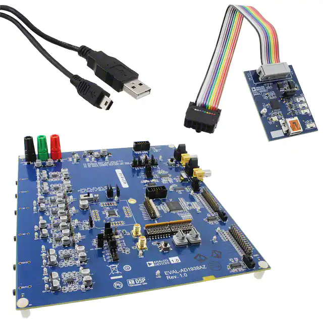
board, EVAL-ADUSB2EBZ (also called USBi), connects to a PC
USB port and provides SPI access to the evaluation board
through a ribbon cable. A graphical user interface (GUI)
program is provided for easy programming of the chip in a
Microsoft® Windows® PC environment. The evaluation board
allows demonstration and performance testing of most AD1938
features, including four ADCs and eight DACs, as well as the
digital audio ports.
EVAL-AD1938AZ PACKAGE CONTENTS
AD1938 evaluation board
USBi control interface board
USB cable
OTHER SUPPORTING DOCUMENTATION
AD1938 data sheet
EVALUATION BOARD OVERVIEW
Additional analog circuitry (ADC input filters, DAC output
filter/buffer) and digital interfaces such as S/PDIF are provided
to ease product evaluation.
This document explains the design and setup of the evaluation
board for the AD1938. The evaluation board must be connected
to an external ±12 V dc power supply and ground. On-board
regulators derive 3.3 V supplies for the AD1938. The AD1938 is
controlled through an SPI interface. A small external interface
All analog audio interfaces are accessible with stereo audio,
3.5 mm TRS connectors.
FUNCTIONAL BLOCK DIAGRAM
POWER SUPPLY
CONTROL
INTERFACE
SPI
S/PDIF
INTERFACE
DAC 1&2
ANALOG
AUDIO
LRCLK, BCLK, SDATA
ADC 1&2
ANALOG
AUDIO
AD1938
SERIAL AUDIO
INTERFACES
DAC 3&4
MCLK ROUTING
CLOCK & DATA ROUTING
08421-001
ANALOG
AUDIO
Figure 1.
PLEASE SEE THE LAST PAGE FOR AN IMPORTANT
WARNING AND LEGAL TERMS AND CONDITIONS.
Rev. 0 | Page 1 of 32
�UG-045
Evaluation Board User Guide
TABLE OF CONTENTS
EVAL-AD1938AZ Package Contents ............................................ 1
Powering the Board.......................................................................3
Other Supporting Documentation ................................................. 1
Setting Up the Master Clock (MCLK)........................................4
Evaluation Board Overview ............................................................ 1
Configuring the PLL Filter ...........................................................5
Functional Block Diagram .............................................................. 1
Connecting Audio Cables ............................................................5
Revision History ............................................................................... 2
Switch and Jumper Settings .........................................................5
Setting Up the Evaluation Board .................................................... 3
Rotary and DIP Switch Settings ......................................................7
Standalone Mode .......................................................................... 3
Schematics and Artwork ..................................................................9
SPI Control .................................................................................... 3
CPLD Code ..................................................................................... 20
Automated Register Window Builder Software Installation .. 3
Ordering Information .................................................................... 26
Hardware Setup, USBi.................................................................. 3
Bill of Materials ........................................................................... 26
REVISION HISTORY
2/10—Revision 0: Initial Version
Rev. 0 | Page 2 of 32
�Evaluation Board User Guide
UG-045
SETTING UP THE EVALUATION BOARD
STANDALONE MODE
It is possible to run the board and the AD1938 codec in standalone mode, which fixes the functionality of the AD1938 into
the I2S data format, running at 256 × fS (default register condition). The ADC BCLK and LRCLK ports are flipped between
slave and master (input and output) by tying SDA/COUT (Pin 24)
to low or high. This is accomplished by moving the J5 jumper to
either 0 or SDA/1 (see Figure 2 and Figure 3 for the correct
settings).
1.
2.
3.
4.
5.
08421-002
1
ADDR1
CLATCH
0
J8
CCLK
ADDR0
0
SCL
1
J7
CIN
0
COUT
0
J6
SDA/1
J5
installation. To install the Automated Register Window
Builder software, follow these steps:
Figure 2. Standalone Slave Mode
J5
J6
J7
J8
At www.analog.com/AD1938, find the Resources & Tools
list.
In the list, find Evaluation Boards & Development Kits
and click Evaluation Boards/Tools to open the provided
ARWBvXX.zip file.
Double-click the provided .msi file to extract the files to an
empty folder on your PC.
Then double-click setup.exe and follow the prompts to
install the Automated Register Window Builder. A
computer restart is not required.
Copy the .xml file for the AD1938 from the extraction
folder into the C:\Program Files\Analog Devices
Inc\AutomatedRegWin folder, if it does not appear in the
folder after installation.
To set up the USBi hardware, follow these steps:
08421-003
ADDR1
CLATCH
1
0
CCLK
0
SCL
ADDR0
CIN
1
0
COUT
0
SDA/1
HARDWARE SETUP, USBi
Figure 3. Standalone Master Mode
With the control jumpers set to standalone slave mode, both
DIP switches, S2 and S3, set to off, and both rotary hex mode
switches, S4 and S5, set to 0, the S/PDIF receiver is the LRCLK,
BCLK, and SDATA source. The default MCLK jumper setting
routes MCLK from the S/PDIF receiver to the AD1938. With a
valid S/PDIF data stream connected to the selected S/PDIF
input port, the board passes audio from the S/PDIF port to all
four stereo outputs and from Stereo IN1 to the S/PDIF output
ports. IN2 can be selected by changing S3, Position 8, to on.
Other serial audio clock and data routing configurations are
described in the Switch and Jumper Settings section.
SPI CONTROL
The evaluation board can be configured for interactive control
of the registers in the AD1938 by connecting the SPI port to the
USBi. The SPI jumper settings are shown in Figure 4.
08421-004
ADDR1
CLATCH
1
0
J8
CCLK
0
SCL
ADDR0
CIN
J7
1
0
COUT
0
J6
SDA/1
J5
Figure 4. SPI Control
The Automated Register Window Builder software controls
the AD1938 and is available at www.analog.com/AD1938.
AUTOMATED REGISTER WINDOW BUILDER
SOFTWARE INSTALLATION
The Automated Register Window Builder is a program that
launches a graphical user interface for direct, live control of the
AD1938 registers. The GUI content for the part is defined in a
part-specific .xml file; this file is included in the software
1.
2.
3.
Plug the USBi ribbon cable into the J1 header.
Connect the USB cable to your computer and to the USBi.
When prompted for drivers, follow these steps:
a. Choose Install from a list or a specific location.
b. Choose Search for the best driver in these locations.
c. Check the box for Include this location in the search.
d. Find the USBi driver in C:\Program Files\Analog
Devices Inc\AutomatedRegWin\USB drivers.
e. Click Next.
f. If prompted to choose a driver, select CyUSB.sys.
g. If the PC is running Windows XP and you receive a
message that the software has not passed Windows
logo testing, click Continue Anyway.
You can now open the Automated Register Window Builder
application and load the .xml file for the part on the evaluation
board.
POWERING THE BOARD
The AD1938 evaluation board requires a power supply input of
±12 V dc and ground to the three binding posts; +12 V draws
~250 mA, and −12 V draws ~100mA. The on-board regulators
provide two 3.3 V rails, one each for AVDD and DVDD for the
AD1938. DVDD also supplies power for the active peripheral
components on the board. Jumpers are provided to allow access
to the power connections of the AD1938. These are convenient
points to insert a current measuring device. The only components on the AD1938 side of the jumper are the part itself and the
local power supply decoupling. The jumper blocks on the
evaluation board are shown in Figure 5.
Rev. 0 | Page 3 of 32
�UG-045
Evaluation Board User Guide
C158
R178
R156
R156
C154 R155
08421-009
R172
EXT CLK IN
JP30
HDR2
JP31
HDR1
R156
OSC
R166
JP24
R175
193X_MCLKO
J23
U22
R174
C168
C170
R175
EXT CLK IN
08421-010
C170
R169
JP28
Figure 10. Passive Crystal; AD1938 Is Master; CPLD Is Slave from
the MCLKO Port
08421-007
C168
R167
JP27
JP29
8416
U18
J22
Y1
JP23
CPLD
U21
JP25
HDR2
EXT CLK
J23
R178
R174
JP20 MCLKO C147
XTAL
OSC DISABLE HDR1
U22
JP28
CLK
R178
193X_MCLKI
DISABLE
MCLKI BUS
R172
EXT CLK IN
JP31
HDR1
C154 R155
08421-006
R169
JP27
OSC DISABLE HDR1
R175
C170
JP30
HDR2
C158
193X_MCLKO
MCLKO BUS
R167
J23
C168
JP18
L7
Y1
JP23
CPLD
U21
JP25
HDR2
MCLKO BUS
R166
JP24
MCLKI BUS
JP29
8416
R160 JP22
J22
R156
C154 R155
MCLKI
XTAL
C153
OSC
U18
193X_MCLKO
U22
R174
1938_MCLKI
JP20 MCLKO C147
XTAL
C158
MCLKI BUS
R172
JP19
1938_MCLKI
R166
R169
C153
MCLKI BUS
EXT CLK IN
C170
193X_MCLKI
DISABLE
JP24
R167
JP27
Figure 6. S/PDIF Receiver as MCLK Master; the AD1938 and CPLD as Slaves
JP31
HDR1
Y1
JP23
CPLD
U21
JP25
HDR2
The MCLK configurations shown in Figure 10 and Figure 11 use
the AD1938 MCLKO port to drive the CPLD and, possibly, the
HDRs. The passive crystal runs the AD1938 at 12.288 MHz.
Figure 11 shows the MCLKI shut off; this is the case when the
PLL is set to LRCLK instead of MCLK.
R175
C168
JP31
HDR1
JP30
HDR2
MCLKI
XTAL
C158
U18
J22
Figure 9. Active On-Board Oscillator as Master; the AD1938 and
CPLD as Slaves
J23
R178
R174
JP30
HDR2
JP29
8416
C153
R160 JP22
L7
MCLKO BUS
JP28
EXT
JP20 MCLKO C147
XTAL
1938_MCLKI
193X_MCLKO
U22
EXT CLK
L7
08421-008
MCLKI BUS
JP19
R178
R172
JP19
JP31
HDR1
MCLKI
XTAL
R169
JP27
OSC DISABLE HDR1
EXT CLK IN
C170
JP30
HDR2
193X_MCLKI
DISABLE
J22
MCLKO BUS
R167
R175
C168
JP18
R156
C154 R155
MCLKI
XTAL
C153
OSC
R166
JP24
U18
J23
Figure 8. External Clock In as Master; the AD1938 and CPLD as Slaves
Y1
JP23
CPLD
U21
JP25
HDR2
R160 JP22
JP29
8416
JP28
C158
JP18
R174
EXT CLK
JP20 MCLKO C147
XTAL
193X_MCLKO
U22
JP28
OSC DISABLE HDR1
1938_MCLKI
JP29
8416
R172
EXT CLK
193X_MCLKI
DISABLE
L7
R169
JP27
OSC DISABLE HDR1
Note that, if the HDR connectors are to be driven with MCLK
from a source on the evaluation board, SW2 and/or SW3 must
be switched from the IN position to the OUT position.
R160 JP22
R167
MCLKO BUS
R166
The evaluation board has a series of jumpers that give the user
great flexibility in the MCLK clock source for the AD1938.
MCLK can come from six different sources: passive crystal,
active oscillator, external clock in, S/PDIF receiver, and two
header connections. Note that the complex programmable logic
device (CPLD) on the board must have a valid clock source; the
frequency is not critical. These jumper blocks can assign the
CPLD clock as well. Most applications of the board use MCLK
from either the S/PDIF receiver or one of the header (HDR)
inputs. Figure 6 to Figure 9 show the on-board active oscillator
disabled so that it does not interfere with the selected clock. The
clock feed to the CPLD comes directly from the clock source.
U18
J22
Y1
JP23
CPLD
U21
JP25
HDR2
JP24
SETTING UP THE MASTER CLOCK (MCLK)
JP19
OSC
R160 JP22
L7
C153
1938_MCLKI
Figure 5. AD1938 Power Jumpers
JP18
JP20 MCLKO C147
XTAL
C154 R155
JP19
OSC
JP7
JP18
08421-005
JP5 JP6
MCLKI
XTAL
193X_MCLKI
DISABLE
DVDD
AVDD1
AVDD2
POWER SELECTION
Figure 7. HDR1 as MCLK Master; the AD1938, CPLD, and HDR2 as Slaves
Rev. 0 | Page 4 of 32
�Evaluation Board User Guide
UG-045
The ADC buffer circuit is designed with a switch (S1) that
allows the user to change the voltage reference for all of the
amplifiers. GND, CM, and FILTR can be selected as a reference;
it is advisable to shut down the power to the board before
changing this switch. The CM and FILTR lines are very
sensitive and do not react well to a change in load while the
AD1938 is active. A series of jumpers allows the user to dccouple the buffer circuit to the ADC analog port when CM and
FILTR are selected (see Figure 14).
MCLK LRCLK
R138
JP15
C131
MCLK LRCLK
JP15
C131
08421-013
C114
PLL SELECT
C120
C125
R138
R87
IN1R
C68
C80
C77
C88
R107
R106
R81
FILTER
CM
VREF SELECT
TP32
C83
C82
U14
C99
GND
JP4
R85
R86
C76
C74
IN1R+
IN1R–
TP34
Figure 14. VREF Selection and DC Coupling Jumpers
There are two types of digital interfacing, S/PDIF and discrete
serial. The input and output S/PDIF ports have optical and
coaxial connectors. The serial audio connectors use 1 × 2 100 mil
spaced headers with pins for both signal and ground. The
LRCLK, BCLK, and SDATA paths are available for both the
ADC and DAC on the HDR1 and HDR2 connectors. Each has a
connection for MCLK; each HDR MCLK interface has a switch
to set the port as an input or output, depending on the master
or slave state of the AD1938.
Figure 12. MCLK Loop Filter Selected
R129
C69
R84
S1
IN1L–
TP28
Digital Audio
08421-012
C114
PLL SELECT
C120
C125
TP25
TP30
The PLL for the AD1938 can run from either MCLK or LRCLK,
according to its setting in the PLL and Clock Control 0 register,
Bits[6:5]. The matching RC loop filter must be connected to LF
(Pin 47) using JP15. See Figure 12 and Figure 13 for the jumper
positions.
U12
IN1L+
08421-014
CONFIGURING THE PLL FILTER
C67
JP12 JP11
Figure 11. LRCLK Is the Master Clock Using the PLL; MCLKI Is Disabled, and
CPLD Is Slave to the MCLKO Port
TP26
C65
C64
R90
IN1L
C61
R76
C60
08421-011
JP31
HDR1
R129
C63
R72
EXT CLK IN
C170
JP30
HDR2
R73
R175
C89
C168
C72
JP29
8416
C105
R178
R174
R101
U22
JP28
EXT CLK
MCLKI BUS
J23
R79R77C62
R172
R93
R97 C79
R169
JP27
OSC DISABLE HDR1
193X_MCLKO
C66
R166
R167
JP13
Y1
JP23
CPLD
U21
JP25
HDR2
JP24
J22
C75
C158
U18
MCLKO BUS
OSC
R160 JP22
L7
C153
1938_MCLKI
R156
JP19
JP20 MCLKO C147
XTAL
C154 R155
MCLKI
XTAL
193X_MCLKI
DISABLE
JP18
SWITCH AND JUMPER SETTINGS
Figure 13. LRCLK Loop Filter Selected
Clock and Control
Normally, the MCLK filter is the default selection; it is also
possible to use the register control window to program the
PLL to run from the LRCLK. In this case, the jumper must
be changed as shown in Figure 13.
CONNECTING AUDIO CABLES
Analog Audio
The analog inputs and outputs use 3.5 mm TRS jacks; they are
configured in the standard configuration: tip = left, ring = right,
sleeve = ground. The analog inputs to IN1 and IN2 generate
0 dBFS from a 1 V rms analog signal. The on-board buffer circuit
creates the differential signal to drive the ADC with 2 V rms at
the maximum level. The DAC puts out a 0.8775 V rms singleended signal at 0 dBFS; this signal is buffered and filtered before
the OUT connectors. There are test points that allow direct
access to the ADC and DAC pins; note that the ADC and DAC
have a common-mode voltage of 1.5 V dc. These test points
require proper care so that improper loading does not drag
down the common-mode voltage, and the headroom and
performance of the part do not suffer.
The AD1938 is designed to run in standalone mode at a sample
rate (fS) of 48 kHz, with an MCLK of 12.288 MHz (256 × fS). In
standalone slave mode, both ADC and DAC ports must receive
valid BCLK and LRCLK. The AD1938 can be clocked from
either the S/PDIF receiver or the HDR1 connector; the ADC
BCLK and LRCK port sources are selected with S2, Position 2
and Position 3. For the S/PDIF master, both switches should be
off. For HDR1, S2, Position 3, should be on (see the detail in
Figure 15 and Figure 16). The DAC BCLK and LRCK port
sources are selected with S2, Position 5 and Position 6. For the
S/PDIF master, both switches should be off. For HDR1, S2,
Position 6, should be on. Note that HDR2 is not implemented
in the CPLD routing code.
It is also possible to configure the AD1938 ADC BCLK and
LRCK ports to run in standalone master mode; moving J5 to
SDA/1, as shown in Figure 3, changes the state of the AD1938.
Setting S2, Position 2 and Position 5, to on selects the proper
routing to both the S/PDIF receiver and the HDR1 connector.
Rev. 0 | Page 5 of 32
�UG-045
Evaluation Board User Guide
In this mode, the AD1938 ADC port generates BCLK and
LRCLK when given a valid MCLK.
For full flexibility of the AD1938, the part can be put in SPI
control mode and programmed with the Automated Register
Window Builder application (see Figure 4 for the appropriate
jumper settings). Changing the registers and setting the DIP
switches allow many possible configurations. In the various
master and slave modes, the AD1938 takes MCLK from a
selected source and can be set to generate or receive either
BCLK or LRCLK to or from either the ADC or the DAC port,
depending on the settings and requirements.
As an example, to set the ADC port as master, switch the ADC
Control 2 register bits for BCLK and LRCLK to master, and
change S2, Position 2 and Position 5, to on. In this mode, the
board is configured so that the ADC BCLK and LRCLK pins are
the clock source for both the ADC destination and the DAC
data source. For the DAC port to be the master, the DAC
Control 1 register bits for BCLK and LRCLK must be changed
to master, and S2, Position 2 and Position 3, and S2, Position 5
and Position 6, must all be on. On this evaluation board, these
settings allow the master port on the AD1938 to drive both the
S/PDIF and the HDR connections. Many combinations of master
and slave are possible (see Figure 15 and Figure 16 for the correct
settings).
S/PDIF Audio
The settings shown in Figure 15 and Figure 16 show the details
of clock routing and control for both the ADC and DAC ports.
The board is shipped with the S/PDIF port selected as the
default; the hex switches are set to 0, and all DIP switches are
set to off. The AD1938 is shipped in standalone mode (see
Figure 2); the BCLK and LRCLK signals run from the S/PDIF
receiver to the ADC and DAC ports of the AD1938.
In this default configuration, the DAC audio path routes the
S/PDIF audio signal to all four stereo AD1938 DSDATA inputs
simultaneously. The rotary switch, S4, allows the user to select
individual stereo pairs for transmission of the analog signal.
Position 0 is the default; Position 1 through Position 4 allow the
S/PDIF input signal to be assigned to Pair 1 to Pair 4, respectively.
Also in this default configuration, the IN1 analog is routed through
the AD1938 ADC ASDATA1 path to the S/PDIF output. IN2 is
selected by changing the S3 DIP switch, Position 8, from 0 to 1.
HDR Connectors—Serial Audio
Routing of serial audio to and from the HDR1 connector is controlled by DIP S3, Position 6 and Position 7, and Rotary S4. For
the DAC audio signal path, S4, Position 8, assigns the data
signal coming into HDR1 DSDATA1 to all four DSDATA ports
on the AD1938. S4, Position 9, assigns the HDR1 labeled ports
to the associated port on the AD1938.
Other Options
It is possible to mute all data going to the DSDATA ports of the
AD1938 by selecting S4, Position 7. This shows the SNR of the
DACs
To use other fS rates, the USBi must be connected and the
AD1938 registers must be programmed accordingly. For
example, adjusting the fS rate to 96 kHz requires that the ADC
and DAC Control 0 registers have sample rates set to 96 kHz
(see Figure 15 and Figure 16 for the complete list of options).
The CPLD code is presented in the CPLD Code section and is
included with the evaluation board; alterations and additions to
the functionality of the CPLD are possible by altering the code
and reprogramming the CPLD.
Rev. 0 | Page 6 of 32
�Figure 15. Settings Chart 1
Rev. 0 | Page 7 of 32
Description
SPDIF_TX_RX RESETB
SPDIF_RX_TX in active mode
SPDIF_RX_TX in reset mode
Position-8
SPDIF_RX_TX /RESET
Off*
On
SPDIF TX - CS8406 Jumpers
JP18
0 = the V pin input determines the s tate of the v alidity bit in the outgoing AES3 transmitted data
1 = the V pin input determines the s tate of the v alidity bit in the outgoing AES3 transmitted data
JP2
0 = NVERR selected
1 = RERR selected
Description
SPDIF_RX_TX MCLK Rate
SPDIF_RX_TX MCLK Rate = 256xfS
SPDIF_RX_TX MCLK Rate = 128xfS
Position-7
SPDIF_RX-TX Clock Rate Selection
Off*
On
SPDIF RX - CS8416 Jumpers
JP1
0 = Normal update rate phase detector, increased clock jitter
1 = High update rate phase detector, low clock jitter
DBCLK Source
SPDIF_RX_8416
HDR1_DBCLK
ADC-ABCLK
DAC-DBCLK
Position-5
Position-6
DAC - DBCL K, DLRCLK Source Selection
Off*
Off*
Off
On
On
Off
On
On
DLRCLK Source
SPDIF_RX_8416
HDR1_DLRCLK
ADC-ALRCLK
DAC-DLRCLK
Enable DAC clocks
Tristate DAC clocks
Description
ALRCLK Source
SPDIF_RX_8416
HDR1_ALRCLK
ADC-ALRCLK
DAC-DLRCLK
Position-4
DAC – DBCLK, DLRCLK Clock Disable
Off*
Enable
On
Disable
Position-2
Position-3
ADC - ABCL K, ALRCLK Source Selection
Off*
Off*
Off
On
On
Off
On
On
ABCLK Source
SPDIF_RX_8416
HDR1_ABCLK
ADC-ABCLK
DAC-DBCLK
Enable ADC clocks
Tristate ADC clocks
Off*
On
Enable
Disable
Description
DIP Switch S2 position:
Position-1
ADC- ABCLK, ALRCLK Clock Disable
SPDIF_Tx Clocks
Slave
Slave
Slave
Slave
SPDIF_Tx Clocks
Slave
Slave
Slave
Slave
HDR1 Clocks
Slave
Master
Slave
Slave
HDR1 Clocks
Slave
Master
Slave
Slave
ADC Cl ocks
N/A
N/A
Master
N/A
ADC Cl ocks
Slave
Slave
Master
Slave
SPDIF_TX CS8406 MCLK Rate Jumper Settings
JP10
JP9
0
0
0
1
JP3
0 = Emphasis audio match off
1 = Emphasis audio match on
SPDIF_TX MCLK Rate = 256xfS
SPDIF_TX MCLK Rate = 128xfS
(Note: This position must be toggled after power-up for proper operation.)
SPDIF_TX CS8406 MCLK Jumper Settings
JP10
JP9
0
0
0
1
SPDIF_Rx Clocks
Master
Slave
Slave
Slave
SPDIF_Rx Clocks
Master
Slave
Slave
Slave
1) DIP Switch S2 controls the AD193x ADC a nd DAC serial clock source selection. One of four clock sources is selected based on the setting. SPDIF Receiver
CS8416, Header Connector HDR1, ADC serial clocks, or DAC serial clock can be the clock source. ADC a nd DAC serial clock selection is controlled independently.
2) The AD193x master clock source should be selected using the JP28, JP29, JP30, and JP31 header jumpers such that the MCLK source is in sync with the DAC/ADC serial clock and data source.
ADC and DAC Serial Clock (BCLK, LRCLK) Source Selection and Routing (Switch S2)
1) DIP Switch S2 Position-8 (SPDIF_RX_TX reset) must be toggled after power-up for proper operation of the SPDIF receiver and transmitter.
2) The AD193x evalution board defaults the AD193x codec to standalone mode preventing SPI/I2C operation. The J5, J6, J7, and J8 he ader jumpers can be changed for SPI/I2C operation.
AD193X/ADAU132X Rev-E Evaluation Board Configuration: (* indicates default setting)
DAC Clocks
Slave
Slave
Slave
Master
DAC Clocks
N/A
N/A
N/A
Master
Evaluation Board User Guide
UG-045
ROTARY AND DIP SWITCH SETTINGS
08421-015
�SPDIF_RX_8416
HDR1_DSDATA2
SPDIF_RX_8416
HDR1_DSDATA2
HDR1_DSDATA2
N/A
N/A
ZERO DATA
HDR1_DSDATA1
HDR1_DSDATA2
DAC_TDM_OUT
DAC_TDM_OUT
Aux ADC1 input
TRISTATE
SPDIF_RX_8416
SPDIF_RX_8416
HDR1_DSDATA1
HDR1_DSDATA1
HDR1_DSDATA1
N/A
N/A
ZERO DATA
HDR1_DSDATA1
HDR1_DSDATA1
HDR1_DSDATA1
HDR1_DSDATA1
HDR1_DSDATA1
TRISTATE
Stereo
Stereo
Stereo
Stereo
Stereo
N/A
N/A
Stereo/TDM
Stereo
Stereo
TDM
Dual- Line TDM
DAC aux mode
Stereo/TDM
TRISTATE
DAC_TDM_OUT
Aux DAC2 output
HDR1_DSDATA3
Aux ADC2 input
TRISTATE
SPDIF_RX_8416
HDR1_DSDATA4
HDR1_DSDATA4
HDR1_DSDATA4
SPDIF_RX_8416
N/A
N/A
ZERO DATA
HDR1_DSDATA1
HDR1_DSDATA4
SPDIF_RX_8416
HDR1_DSDATA3
HDR1_DSDATA3
SPDIF_RX_8416
HDR1_DSDATA3
N/A
N/A
ZERO DATA
HDR1_DSDATA1
HDR1_DSDATA3
0*
1
2
3
4
5
6
7
8
9
A
B
C
D
E
F
Figure 16. Settings Chart 2
Rev. 0 | Page 8 of 32
Input
Input
Input
Output
Output
Input
TRISTATE
Input
Input
Input
Input
Input
Input
TRISTATE
Position-7
Off*
On
Off
On
ADC Serial Format
Stereo
Stereo
TDM
ADC Aux (see note)
HDR1_ ASDATA1
ASDATA1
ASDATA2
ASDATA1
ASDATA1
TRISTATE
Output
Output
Input
Input
TRISTATE
Input
Input
Input
Input
Input
Input
Input
Input
Input
Input
Input
Input
Input
Input
Input
Input
HDR1_ ASDATA1
Output
Output
Output
Output
HDR1_ ASDATA2
Output
Output
Input
Input
DIP Switch S3 Position:
Position-8
Off*
ADC1 Data Stream ASDATA1 is sourced to the SPDIF_Tx_8406.
On
ADC2 Data Stream ASDATA2 is sourced to the SPDIF_Tx_8406.
DIP Switch S3 Position:
Position-6
Position-7
Off*
Off*
Off
On
On
Off
On
On
NOTE: ADC A UX mode overrides the DAC data configuration rotary Switch S2 setting.
Position-6
Off*
Off
On
On
DIP Switch S3 Position:
Input
Input
Input
Input
Input
Input
Input
Input
Input
Input
ADC1 (ASDATA1)
Output
Output
Output
Output
HDR1_ ASDATA2
ASDATA2
ASDATA2
ADC TDM input stream
ADC TDM input stream
Output
Input
Input
Input
Input
Input
N/A
N/A
Input
Input
Input
***** Column content indicates the direction of the DAC data pins and corresponding HDR1 connector DAC data pins *******
DAC2 (DSDATA2)
DAC3 (DSDATA3)
DAC4 (DSDATA4)
HDR 1_DSDATA1
S4 Position DAC1 (DSDATA1)
0*
1
2
3
4
5
6
7
8
9
A
B
C
D
E
F
***** Signal sources to the DAC data lines (DSDATA1/2/3/4) fill the columns, column header is the destination ******
S4 Position DAC Serial Format
DAC1 (DSDATA1)
DAC2 (DSDATA2)
DAC3 (DSDATA3)
DAC4 (DSDATA4)
Input
Input
Output
Input
Input
N/A
Input
Input
N/A
Input
HDR 1_DSDATA3
Output
Output
Output
Input
Input
N/A
Input
Input
Input
N/A
HDR 1_DSDATA4
N/A
Master
Master
Master
Master
Master
SPDIF_Rx Data
N/A
Master
Master
Master
Master
Master
HDR 1 Data
ADC2 (ASDATA2)
Output
Output
Input
Input
Description (HDR1 ADC Data Source Selection)
HDR1 Connector ADC Data Lines ASDATA1 and ASDATA2 receive corresponding ADC data stream
HDR1 Connector ADC Data Line ASDATA1 receive ADC2 data line ASDATA2
HDR1 Connector ADC Data Line ASDATA1 receive ADC TDM out data stream
HDR1 Connector ADC Data Line ASDATA1 receive ADC TDM out data stream
Output
Input
Input
Output
Output
Input
N/A
Input
N/A
Input
Input
HDR 1_DSDATA2
Tristate all DAC data lines, DSDATA1, DSDATA2, DSDATA3, and DSDATA4
Source zero data to all eight DAC channels
HDR1 Connector Signal HDR1_D SDATA1 drives all four DAC pairs
HDR1 Connector Data Lines DSDATA1, DSDATA2... so on drive corresponding DAC data lines
HDR1 Connector Data Lines DSDATA1, DSDATA2... so on drive/receive corresponding DAC data lines in TDM mode
HDR1 Connector Data Lines DSDATA1, DSDATA2... so on drive/receive corresponding DAC data lines in TDM mode
HDR1 Connector Data Lines DSDATA1, DSDATA2... so on drive/receive corresponding DAC data lines in TDM mode
SPDIF_RX_8416 stereo data to all eight DAC channels
SPDIF_RX_8416 stereo data to DAC1 only, rest DACs2/3/4 data from HDR1 connector
SPDIF_RX_8416 data to DAC2 only, rest DACs1/3/4 data from HDR1 connector
SPDIF_RX_8416 data to DAC3 only, rest DACs1/2/4 data from HDR1 connector
SPDIF_RX_8416 data to DAC4 only, rest DACs1/2/3 data from HDR1 connector
Description
08421-016
Rotary hex Switch S4 selects the AD193x DAC serial data source. The DAC data source can be either SPDIF Receiver CS8416 or can be provided by the Header Connector HDR1. It is important to note that the DAC data source should be in sync with the DAC
serial port clock source( set by DIP Switch S2, Positions [5:6]. DIP Switch S3 routes the ADC serial data among AD193x, SPDIF Transmitter CS8406, and Header Connector HDR1 in stereo, TDM, and aux mode.
DAC and ADC Se rial Data (DSDATA/ASDATA) Source Selection and Routing (Switch S4 and S witch S3)
UG-045
Evaluation Board User Guide
�Evaluation Board User Guide
UG-045
SCHEMATICS AND ARTWORK
08421-017
Figure 17. Board Schematics, Page 1—ADC Buffer Circuits
Rev. 0 | Page 9 of 32
�UG-045
Evaluation Board User Guide
08421-018
Figure 18. Board Schematics, Page 2—Serial Digital Audio Interface Headers with MCLK Direction Switching
Rev. 0 | Page 10 of 32
�Evaluation Board User Guide
UG-045
08421-019
Figure 19. Board Schematics, Page 3—S/PDIF Receive and Transmit Interfaces
Rev. 0 | Page 11 of 32
�UG-045
Evaluation Board User Guide
08421-020
Figure 20. Board Schematics, Page 4—Serial Digital Audio Routing and Control CPLD
Rev. 0 | Page 12 of 32
�Evaluation Board User Guide
UG-045
08421-021
Figure 21. Board Schematic, Page 5—AD1938 with MCLK Selection Jumpers
Rev. 0 | Page 13 of 32
�Evaluation Board User Guide
08421-022
UG-045
Figure 22. Board Schematics, Page 6—Daughter Card Interface, Useful as Test Points
Rev. 0 | Page 14 of 32
�Evaluation Board User Guide
UG-045
08421-023
Figure 23. Board Schematics, Page 7—DAC Buffer Circuits
Rev. 0 | Page 15 of 32
�UG-045
Evaluation Board User Guide
08421-024
Figure 24. Board Schematics, Page 8—SPI Control Interface
Rev. 0 | Page 16 of 32
�UG-045
08421-025
Evaluation Board User Guide
Figure 25. Board Schematics, Page 9—Power Supply
Rev. 0 | Page 17 of 32
�Evaluation Board User Guide
08421-026
UG-045
Figure 26. Top Assembly Layer
Rev. 0 | Page 18 of 32
�UG-045
08421-027
Evaluation Board User Guide
Figure 27. Bottom Assembly Layer
Rev. 0 | Page 19 of 32
�UG-045
Evaluation Board User Guide
CPLD CODE
MODULE
TITLE
IF_Logic
'AD1938 EVB Input Interface Logic'
//===================================================================================
//
FILE:
//
REVISION DATE:
AD1938_pld_revE.abl
//
REVISION:
//
DESCRIPTION:
04-16-09 (rev-E)
E
//===================================================================================
LIBRARY 'MACH';
"INPUTS
----------------------------------------------------------------------------
// AD1938 CODEC pins
DSDATA1,DSDATA2
pin 86, 87 istype 'com';
DSDATA3,DSDATA4
pin 91, 92 istype 'com';
DBCLK,DLRCLK
pin 85, 84 istype 'com';
ASDATA1,ASDATA2
pin 80, 81 istype 'com';
ABCLK,ALRCLK
pin
78, 79 istype 'com';
// 25-pin header connector HDR1 pins
HDR1_DSDATA1
pin 20 istype 'com';
HDR1_DSDATA2
pin 19 istype 'com';
HDR1_DSDATA3
pin 17 istype 'com';
HDR1_DSDATA4
pin 16 istype 'com';
HDR1_DBCLK
pin 21 istype 'com';
HDR1_DLRCLK
pin 22 istype 'com';
HDR1_ASDATA1
pin 29 istype 'com, buffer';
HDR1_ASDATA2
pin
28 istype 'com, buffer';
HDR1_ABCLK
pin
30 istype 'com';
HDR1_ALRCLK
pin
31 istype 'com';
// 25-pin header connector HDR2 pins
HDR2_DSDATA1
pin
HDR2_DSDATA2
pin 36 istype 'com';
37 istype 'com';
HDR2_DSDATA3
pin 35 istype 'com';
HDR2_DSDATA4
pin 34 istype 'com';
HDR2_DBCLK
pin
41 istype 'com';
HDR2_DLRCLK
pin
42 istype 'com';
HDR2_ASDATA1
pin 44 istype 'com';
HDR2_ASDATA2
pin 43 istype 'com, buffer';
HDR2_ABCLK
pin
47 istype 'com';
HDR2_ALRCLK
pin
48 istype 'com';
// S/PDIF Rx CS8414 pins
SDATA_8416
pin 61 istype 'com';
Rev. 0 | Page 20 of 32
�Evaluation Board User Guide
UG-045
BCLK_8416
pin 60 istype 'com';
LRCLK_8416
pin 59 istype 'com';
SOMS_RX,SFSEL1_RX,SFSEL0_RX,RMCKF_RX
pin 66,67,64,65 istype 'com';
// S/PDIF Tx CS8404 pins
SDATA_8406
'com';
pin 50 istype
BCLK_8406,LRCLK_8406
pin 53, 54 istype 'com';
MCLK_8406
'com';
pin 49 istype
APMS_TX,SFMT1_TX,SFMT0_TX
pin 55,56,58 istype 'com';
CPLD_MCLK
'com';
pin
89 istype
// AD1938 SPI port pins
//CCLK,CDATA,CLATCH
pin 84, 83, 85 istype 'com';
//COUT
pin 82 istype 'com';
//CLATCH2,CLATCH3,CLATCH4
pin 86, 56, 4 istype 'com';
//CONTROL_ENB
'com';
pin 81 istype
S/PDIF_RESET_OUT
'com';
pin 69 istype
// Switch S1, S2, S3 and S4 pins
ADC_CLK_OFF
'com';
pin 93 istype
// S2-1
ADC_CLK_SRC1
pin 94 istype 'com';
// S2-2
ADC_CLK_SRC0
pin 97 istype 'com';
// S2-3
DAC_CLK_OFF
'com';
pin 98 istype
// S2-4
DAC_CLK_SRC1
pin 99 istype 'com';
DAC_CLK_SRC0
pin 100 istype 'com';
S/PDIF_MCLK_RATE
pin 3 istype 'com';
// S2-7
S/PDIF_RESET_IN
pin 4 istype 'com';
MODE11,MODE12,MODE13,MODE14
STAND_ALONE,MODE22,MODE23,MODE24
// S2-8
pin 5,6,8,9 istype 'com'; // S4
pin 10,11,14,15 istype 'com'; // S5
"NODES
I_DSDATA1, I_DSDATA2, I_DSDATA3, I_DSDATA4
node istype 'com';
I_DBCLK, I_DLRCLK
node istype 'com';
I_ASDATA1, I_ASDATA2
node istype 'com, buffer';
I_ABCLK, I_ALRCLK
node istype 'com';
Qdivide
// S2-5
// S2-6
node istype 'reg, buffer';
Rev. 0 | Page 21 of 32
�UG-045
Evaluation Board User Guide
//================================================================================
"MACROS
// Switch S3, DIP POSITIONS 6 AND 7
ADC_HDR_NORMAL
= ( MODE22 &
MODE23);
ADC_HDR_DATA2_DATA1 = ( MODE22 & !MODE23);
ADC_HDR_TDM
= (!MODE22 &
MODE23);
ADC_HDR_AUX
= (!MODE22 & !MODE23);
S/PDIF_OUT_MUX = MODE24;
// HEX Switch S4
// S4 position 0,
DAC_RX_ALL
=
( MODE14 & MODE13 &
MODE12 &
MODE11);
// S4 position 1,
DAC_RX_1
=
( MODE14 & MODE13 &
MODE12 &
!MODE11);
// S4 position 2,
DAC_RX_2
=
( MODE14 & MODE13 &
DAC_RX_3
=
( MODE14 & MODE13 &
!MODE12 &
MODE11);
// S4 position 3,
!MODE12 &
!MODE11);
// S4 position 4,
DAC_RX_4 =
( MODE14 & !MODE13 &
MODE12 &
MODE11);
// S4 position 5,
NA1
=
( MODE14 & !MODE13 &
NA2
=
( MODE14 & !MODE13 &
MODE12 &
!MODE11);
// S4 position 6,
!MODE12 &
MODE11);
// S4 position 7,
DAC_DATA_ZERO
=
( MODE14 & !MODE13 &
!MODE12 &
!MODE11);
// S4 position 8,
DAC_HDR1_ALL
=
( !MODE14 & MODE13 &
DAC_HDR1_IND
=
( !MODE14 & MODE13 &
MODE12 &
MODE11);
// S4 position 9,
MODE12 &
!MODE11);
// S4 position A,
DAC_HDR1_TDM
=
( !MODE14 & MODE13 &
!MODE12 &
MODE11);
Rev. 0 | Page 22 of 32
�Evaluation Board User Guide
UG-045
// S4 position B,
DAC_DUAL_TDM
=
( !MODE14 & MODE13 &
DAC_HDR1_AUX
=
( !MODE14 & !MODE13 &
!MODE12 &
!MODE11);
// S4 position C,
MODE12 &
MODE11);
// S4 position D,
NA3
=
( !MODE14 & !MODE13 &
MODE12 &
!MODE11);
// S4 position E,
NA4
=
( !MODE14 & !MODE13 &
!MODE12 &
MODE11);
// S4 position F,
DAC_DATA_HIZ
=
( !MODE14 & !MODE13 &
!MODE12 &
!MODE11);
// Switch S2
DAC_S/PDIF = (DAC_CLK_SRC1 & DAC_CLK_SRC0);
DAC_HDR1
= (DAC_CLK_SRC1 & !DAC_CLK_SRC0);
DAC_ADC
= (!DAC_CLK_SRC1 & DAC_CLK_SRC0);
DAC_DAC
= (!DAC_CLK_SRC1 & !DAC_CLK_SRC0);
ADC_S/PDIF = (ADC_CLK_SRC1 & ADC_CLK_SRC0);
ADC_HDR1
= (ADC_CLK_SRC1 & !ADC_CLK_SRC0);
ADC_ADC
= (!ADC_CLK_SRC1 & ADC_CLK_SRC0);
ADC_DAC
= (!ADC_CLK_SRC1 & !ADC_CLK_SRC0);
"====================================================================================
EQUATIONS
S/PDIF_RESET_OUT = S/PDIF_RESET_IN;
// Configuration of the CS8416, changes active on reset, BCLK_8416 and LRCLK_8416 are bidirectional signals.
SOMS_RX
=
DAC_S/PDIF;
// SOMS = Serial Output Master/Slave Select
SFSEL1_RX
=
0; //DIR_RJ # DIR_RJ16;
// SFSEL1 = Serial Format Select 1
SFSEL0_RX
=
1; //DIR_I2S # DIR_DSP;
// SFSEL0 = Serial Format Select 0
RMCKF_RX
=
!S/PDIF_MCLK_RATE;
// RMCKF =
Receive Master Clock Frequency
//
M0_8414 = (0 # !DAC_S/PDIF);
//
M1_8414 = 1;
//
M2_8414 = 0;
Rev. 0 | Page 23 of 32
�UG-045
//
Evaluation Board User Guide
M3_8414 = 0;
// CS8404 Tx interface mode select
APMS_TX = 0; // Tx serial port is always slave in this application
SFMT1_TX = 0;
// Tx data format is I2S always
SFMT0_TX = 1;
//
M0_8404 = 0;
//
M1_8404 = 0;
//
M2_8404 = 1;
// I2S format only
// divide 256Fs clock by 2 for 128Fs clock to the the S/PDIF Tx
//
Qdivide.clk =
CPLD_MCLK;
//
Qdivide.d = !Qdivide;
//
MCLK_8406 = Qdivide;
MCLK_8406 = CPLD_MCLK;
BCLK_8406 = I_ABCLK;
LRCLK_8406 = I_ALRCLK;
SDATA_8406 = (ASDATA1 & S/PDIF_OUT_MUX) # (ASDATA2 & !S/PDIF_OUT_MUX);
// For SPI mode, let external port drive the SPI port
DBCLK.oe
= (DAC_S/PDIF
# DAC_HDR1 # DAC_ADC # !DAC_DAC) & (DAC_CLK_OFF);
DLRCLK.oe = (DAC_S/PDIF
# DAC_HDR1 # DAC_ADC # !DAC_DAC) & (DAC_CLK_OFF);
ABCLK.oe
= (ADC_S/PDIF
# ADC_HDR1 # !ADC_ADC # ADC_DAC) & (ADC_CLK_OFF);
ALRCLK.oe = (ADC_S/PDIF
# ADC_HDR1 # !ADC_ADC # ADC_DAC) & (ADC_CLK_OFF);
HDR1_DBCLK.oe
= (DAC_S/PDIF
# !DAC_HDR1 # DAC_ADC # DAC_DAC);
HDR1_DLRCLK.oe = (DAC_S/PDIF
# !DAC_HDR1 # DAC_ADC # DAC_DAC);
HDR1_ABCLK.oe
= (ADC_S/PDIF
# !ADC_HDR1 # ADC_ADC # ADC_DAC);
HDR1_ALRCLK.oe = (ADC_S/PDIF
# !ADC_HDR1 # ADC_ADC # ADC_DAC);
BCLK_8416.oe
= (!DAC_S/PDIF);
LRCLK_8416.oe = (!DAC_S/PDIF);
BCLK_8416
= I_DBCLK;
LRCLK_8416
= I_DLRCLK;
DSDATA1.oe
= (!DAC_DATA_HIZ);
DSDATA2.oe = (!(DAC_HDR1_TDM # DAC_DUAL_TDM # DAC_DATA_HIZ));
TDM-daisy chain mode
DSDATA3.oe
//DSDATA2 is output in DAC
= (!DAC_DATA_HIZ);
DSDATA4.oe = (!(DAC_DUAL_TDM # ADC_HDR_AUX # DAC_HDR1_AUX # DAC_DATA_HIZ));
TDM-OUT IN DUAL LINE DAC TDM MODE
ASDATA2.oe
= (ADC_HDR_TDM);
//ASDATA2 is input in ADC TDM mode
HDR1_DSDATA2.oe = (DAC_HDR1_TDM # DAC_DUAL_TDM);
Rev. 0 | Page 24 of 32
// SECOND
�Evaluation Board User Guide
UG-045
HDR1_DSDATA4.oe = (DAC_DUAL_TDM # ADC_HDR_AUX # DAC_HDR1_AUX);
HDR1_ASDATA2.oe = (!ADC_HDR_TDM);
DBCLK
= I_DBCLK;
DLRCLK
= I_DLRCLK;
ABCLK
= I_ABCLK;
ALRCLK
= I_ALRCLK;
DSDATA1 = (HDR1_DSDATA1 & (DAC_HDR1_ALL # DAC_HDR1_IND # DAC_RX_2 # DAC_RX_3 # DAC_RX_4 #
DAC_HDR1_TDM # DAC_DUAL_TDM # ADC_HDR_AUX))
# (SDATA_8416 & (DAC_RX_ALL # DAC_RX_1)) # (0 & DAC_DATA_ZERO);
DSDATA2 = (HDR1_DSDATA1 & DAC_HDR1_ALL) # (HDR1_DSDATA2 & (DAC_HDR1_IND # ADC_HDR_AUX #
DAC_HDR1_AUX # DAC_RX_1 # DAC_RX_3 # DAC_RX_4))
# (SDATA_8416 & (DAC_RX_ALL # DAC_RX_2)) # (0 & DAC_DATA_ZERO);
DSDATA3 = (HDR1_DSDATA1 & (DAC_HDR1_ALL)) # (HDR1_DSDATA3 & (DAC_HDR1_IND # DAC_DUAL_TDM #
ADC_HDR_AUX # DAC_HDR1_AUX # DAC_RX_1 # DAC_RX_2 # DAC_RX_4))
# (SDATA_8416 & (DAC_RX_ALL # DAC_RX_3)) # (0 & DAC_DATA_ZERO);
DSDATA4 = (HDR1_DSDATA1 & (DAC_HDR1_ALL)) # (HDR1_DSDATA4 & (DAC_HDR1_IND # DAC_RX_1 #
DAC_RX_2 # DAC_RX_3))
# (SDATA_8416 & (DAC_RX_ALL # DAC_RX_4)) # (0 & DAC_DATA_ZERO);
HDR1_DBCLK
= I_DBCLK;
HDR1_DLRCLK = I_DLRCLK;
HDR1_ABCLK
= I_ABCLK;
HDR1_ALRCLK = I_ALRCLK;
HDR1_ASDATA1 = (ASDATA1 & (ADC_HDR_NORMAL # ADC_HDR_TDM # ADC_HDR_AUX # DAC_HDR1_AUX )) #
(ASDATA2 & ADC_HDR_DATA2_DATA1);
HDR1_ASDATA2 = ASDATA2;
ASDATA2 = HDR1_ASDATA2;
HDR1_DSDATA2 = DSDATA2;
HDR1_DSDATA4 = DSDATA4;
// Internal node signals
I_DBCLK
= (BCLK_8416 & DAC_S/PDIF) # (HDR1_DBCLK & DAC_HDR1) # (DBCLK & DAC_DAC) #
(I_ABCLK & DAC_ADC);
I_DLRCLK = (LRCLK_8416 & DAC_S/PDIF) # (HDR1_DLRCLK & DAC_HDR1) # (DLRCLK & DAC_DAC) #
(I_ALRCLK & DAC_ADC);
I_ABCLK
= (BCLK_8416 & ADC_S/PDIF) # (HDR1_ABCLK & ADC_HDR1) # (ABCLK & ADC_ADC) #
(I_DBCLK & ADC_DAC);
I_ALRCLK = (LRCLK_8416 & ADC_S/PDIF) # (HDR1_ALRCLK & ADC_HDR1) # (ALRCLK & ADC_ADC) #
(I_DLRCLK & ADC_DAC);
"====================================================================================
END IF_Logic
Rev. 0 | Page 25 of 32
�UG-045
Evaluation Board User Guide
ORDERING INFORMATION
BILL OF MATERIALS
Table 1.
Qty
18
46
9
12
8
16
1
32
3
12
Designator
C85, C90 to C94, C101 to C103,
C107, C108, C110, C115, C116,
C121, C127, C132, C134
C2, C5, C8 to C10, C20, C21, C28,
C29, C38, C42, C48 to C51, C58 to
C60, C62, C64, C69, C73, C76, C79,
C82, C99, C112, C118, C128, C135,
C146, C147, C149, C151, C155,
C156, C158, C162, C168, C174,
C176, C177, C193, C194, C197,
C203
C37, C65, C67, C83, C88, C124,
C129, C157, C160
R28, R30, R51, R59, R166, R167,
R169, R172, R185, R189, R212,
R214
C68, C71, C87, C89, C130, C138,
C159, C161
R24, R31, R44, R60, R77, R84, R93,
R106, R136, R149, R159, R170,
R180, R191, R207, R217
C84
R6, R7, R13, R14, R18, R20, R40,
R43, R47 to R49, R54, R55, R63,
R64, R74, R78, R80, R82, R102,
R117, R158, R164, R173, R176,
R177, R184, R186, R224 to R227
C6, C39, C40
2
C15 to C17, C81, C86, C95, C98,
C170, C175, C178, C180, C183
C104, C106, C109, C111, C117,
C123, C140 to C145
C4, C74
4
C61, C77, C113, C150
3
9
1
D1, D3, D4
C23, C33, C43, C55, C114, C166,
C184, C188, C200
C36
2
C153, C154
8
R76, R81, R90, R101, R134, R141,
R157, R168
R4
12
2
10
R91, R94, R98, R99, R108, R109,
R114, R115, R118, R123
Description
Multilayer ceramic capacitor,16 V, X7R
(0402)
Manufacturer
Panasonic EC
Part Number
ECJ-0EX1C104K
Multilayer ceramic capacitor, 50 V, X7R
(0603)
Panasonic EC
ECJ-1VB1H104K
Multilayer ceramic capacitor, 50 V, NP0
(0603)
Chip resistor, 100 kΩ, 1%, 125 mW, thick
film (0603)
Panasonic EC
ECJ-1VC1H102J
Panasonic EC
ERJ-3EKF1003V
Panasonic EC
ECJ-1VC1H101J
Panasonic EC
ERJ-3EKF1000V
Panasonic EC
EEE-FC1C101P
Panasonic EC
ERJ-3EKF1002V
TDK Corp
C1608C0G1E103J
Panasonic EC
ECJ-1VC2A100D
Kemet
C0402C100J5GACTU
Panasonic EC
EEE-FC1C100R
Panasonic EC
ECJ-1VC1H121J
ON Semiconductor
Murata Electronics
1SMB15AT3G
GRM1885C1H222JA01D
Murata ENA
GRM21B5C1H223JA01L
Panasonic EC
ECJ-1VC1H220J
Panasonic EC
ERJ-3EKF2370V
Panasonic EC
ERJ-3EKF2430V
Rohm
MCR01MZPF24R9
Multilayer ceramic capacitor, 50 V, NP0
(0603)
Chip resistor, 100 kΩ, 1%, 100 mW, thick
film (0603)
Aluminum electrolytic capacitor, 100 μF,
16 V, FC, 105 deg, SMD_E
Chip resistor, 10 kΩ, 1%, 125 mW, thick film
(0603)
Multilayer ceramic capacitor, 25 V, NP0
(0603)
Multilayer ceramic capacitor, 100 V, NP0
(0603)
Multilayer ceramic capacitor, 50 V, NP0
(0402)
Aluminum electrolytic capacitor, 16 V, FC,
105 deg, SMD_B
Multilayer ceramic capacitor, 50 V, NP0
(0603)
TVS Zener, 15 V, 600 W, SMB
Multilayer ceramic capacitor, 50 V, NP0
(0603)
Multilayer ceramic capacitor, 25 V, NP0
(0805)
Multilayer ceramic capacitor, 50 V, NP0
(0603)
Chip resistor, 237 Ω, 1%, 125 mW, thick film
(0603)
Chip resistor, 243 Ω, 1%, 100 mW, thick film
(0603)
Chip resistor, 24.9 Ω, 1%, 63 mW, thick film
(0402)
Rev. 0 | Page 26 of 32
�Evaluation Board User Guide
Qty
16
3
Designator
R56, R57, R65, R66, R88, R89, R140,
R154, R179, R183, R213, R216,
R228 to R231
C25, C31, C45, C53, C169, C181,
C190, C198
R3, R11, R58
1
C125
4
R5, R52, R53, R75
1
C120
33
R38
1
R129
8
3
C24, C34, C44, C56, C167, C185,
C189, C201
C11, C14, C22, C26, C27, C30, C32,
C35, C41, C46, C47, C52, C54, C57,
C63, C66, C72, C75, C80, C105,
C119, C133, C139, C148, C152,
C164, C172, C179, C191, C196
C12, C18, C19
4
R83, R96, R148, R163
20
1
R103, R104, R110 to R112, R116,
R119, R124, R126 to R128, R130 to
R132, R142 to R147
R8 to R10, R15 to R17, R19, R92,
R95, R100, R105, R113, R120, R125,
R133, R135, R139, R153, R155,
R156, R160, R174, R175, R178,
R187, R188, R190, R194, R196,
R200, R201, R203, R206, R210,
R215
R25, R26, R32, R34, R45, R46, R61,
R68, R181, R182, R192, R195, R208,
R209, R218, R220
R21 to R23, R27, R33, R35 to R37,
R39, R41, R42, R50, R62, R69 to
R71
C131
1
R138
16
4
R72, R73, R79, R85 to R87, R97,
R107, R121, R122, R137, R150 to
R152, R165, R171
C78, C137, C171, C195
1
2
1
U11
U19, U26
R29
1
R67
8
30
35
16
16
UG-045
Description
Chip resistor, 24.9 Ω, 1%, 100 mW, thick film
(0603)
Manufacturer
Rohm
Part Number
MCR03EZPFX24R9
Multilayer ceramic capacitor, 50 V, NP0
(0603)
Chip resistor, 374 Ω, 1%, 100 mW, thick film
(0603)
Multilayer ceramic capacitor, 50 V, NP0
(0603)
Chip resistor, 392 Ω, 1%, 100 mW, thick film
(0603)
Multilayer ceramic capacitor, 16 V, ECH-U
(1206)
Chip resistor, 3.01 kΩ, 1%, 100 mW, thick
film (0603)
Chip resistor, 3.32 kΩ, 1%, 100 mW, thick
film (0603)
Multilayer ceramic capacitor, 50 V, NP0
(0603)
Aluminum electrolytic capacitor, 16 V,
FC, 105 deg, SMD_D
Rohm
MCH185A271JK
Rohm
MCR03EZPFX3740
Panasonic EC
ECJ-1VC1H391J
Rohm
MCR03EZPFX3920
Panasonic EC
ECH-U1C393JB5
Rohm
MCR03EZPFX3011
Rohm
MCR03EZPFX3321
Murata ENA
GRM1885C1H431JA01D
Panasonic EC
EEE-FC1C470P
Panasonic EC
EEE-FC1E470P
Panasonic EC
ERJ-3EKF4992V
Rohm
MCR01MZPF49R9
Chip resistor, 49.9 kΩ, 1%, 100 mW, thick
film (0603)
Panasonic EC
ERJ-3EKF49R9V
Chip resistor,49.9 kΩ, 1%, 100 mW, thick
film (0603)
Panasonic EC
ERJ-3EKF4641V
Chip resistor,49.9 kΩ, 1%, 100 mW, thick
film (0603)
Panasonic EC
ERJ-3EKF4751V
Multilayer ceramic capacitor, 25 V, NP0
(0603)
Chip resistor, 562 Ω, 1%, 125 mW, thick film
(0603)
Chip resistor, 5.76 kΩ, 1%, 125 mW, thick
film (0603)
TDK Corp
C1608C0G1E562J
Panasonic EC
ERJ-3EKF5620V
Panasonic EC
ERJ-3EKF5761V
Panasonic EC
ECJ-1VC2A680J
NXP Semi
Texas Instruments
Panasonic EC
74HC04D-T
SN74LV125AD
ERJ-3EKF75R0V
Rohm
MCR03EZPFX90R9
Aluminum electrolytic capacitor, FC,
105 deg, SMD_E
Chip resistor, 49.9 kΩ, 1%, 100 mW, thick
film (0603)
Chip resistor, 49.9 kΩ, 1%, 63 mW, thick film
(0402)
Multilayer ceramic capacitor, 100 V, NP0
(0603)
IC inverter hex ,TTL/LSTTL, 14 SOIC
IC buffer, quad three-state ,14 SOIC
Chip resistor, 75 Ω, 1%, 100 mW, thick film
(0603)
Chip resistor, 90.9 Ω, 1%, 100 mW, thick film
(0603)
Rev. 0 | Page 27 of 32
�UG-045
Evaluation Board User Guide
Qty
1
Designator
Y1
Description
Crystal, 12.288 MHz, SMT, 10 pF
Manufacturer
Abracon Corp
1
U15
Analog Devices
1
1
1
U23
U1
J2
1
J3
1
J4
2
1
J22, J23
U8
1
U13
2
1
1
6
1
2
4
1
D2, D5
S1
SW1
L2 to L7
L1
J1, J14
J15 to J18
J19
Four ADC/eight DAC with PLL, 192 kHz, 24bit CODEC
Microprocessor voltage supervisor
Voltage regulator low dropout
5-way binding post, black, uninsulated,
base TH
5-way binding post, mini, green,
uninsulated, base TH
5-way binding post, mini, red, uninsulated,
base TH
SMA receptacle, straight PCB mount
192 kHz digital audio receiver (DGTL RCVR
28-TSSOP)
192 kHz digital audio interface (S/PDIF
transmitter)
Passivated rectifier, 1 A, 50 V, MELF
Switch slide DP3T PC MNT, L = 4 mm
DPDT slide switch, vertical
Chip ferrite bead, 600 Ω at 100 MHz
Chip ferrite bead, 600 Ω at 100 MHz
10-way shrouded polarized header
16-way unshrouded, not populated
Connector header, 0.100 dual STR, 72 POS
2
J20, J26
Connector header, 0.100 dual STR, 72 POS
Sullins
4
J5 to J8
Connector header, 0.100 dual STR, 72 POS
Sullins
2
19
16-position rotary switch, hex
2-pin header, unshrouded jumper, 0.10";
use shunt Tyco 881545-2
APEM
Sullins
3-position SIP header
Sullins
1
S4, S5
JP4 to JP7, JP11 to JP14, JP17,
JP18, JP20 to JP22, JP24, JP26,
JP28 to JP31
JP1 to JP3, JP8 to JP10, JP15, JP19,
JP23, JP25, JP27
U16
1
D11
Lattice
Semiconductor
Lumex Opto
SML-LX1206GW-TR
2
D6, D9
Lumex Opto
SML-LX1206IW-TR
2
D7, D10
1
U2, U3
J10, J11, J13, J21, J27, J28
R161, R162
U6, U9, U12, U14, U17, U20, U24,
U25
U21
CML Innovative
Tech
STMicroelectronics
CUI
CTS
Analog Devices
CMD15-21VYD/TR8
2
6
2
8
Complex programmable logic devices
(CPLD), HI PERF E2CMOS PLD
Green diffused, 10 millicandela, 565 nm
(1206)
Red diffused, 6.0 millicandela, 635 nm
(1206)
Yellow diffused, 4.0 millicandela, 585 nm
(1206)
3-term adjustable voltage regulator, DPak
Sterero mini jack ,SMT
Resistor network, bussed 9 res
Dual bipolar/JFET audio op amp.
Abracon Corp
AP3S-12.288MHz-F-J-B
2
J9, J12
12.288 MHz, fixed SMD oscillator ,1.8 V dc to
3.3 V dc
RCA jack, PCB, TH mount, R/A, yellow
CTP-021A-S-YEL
1
U10
110 Ω AES/EBU transformer
2
1
U18, U22
U4
Buffer, three-state single gate
Octal, three-state buffer/driver
Connect-Tech
Products
Scientific
Conversion
Texas Instruments
Texas Instruments
11
Rev. 0 | Page 28 of 32
Part Number
ABM3B-12.288MHZ-101-U-T
AD1938YSTZ
Analog Devices
Analog Devices
Deltron
Components
Deltron
Components
Deltron
Components
Amp-RF Division
Cirrus Logic
ADM811RARTZ-REEL7
ADP3303ARZ-3.3
552-0100 BLK
Cirrus Logic
CS8406-CZZ
Micro Commercial
E-Switch
E-Switch
TDK
Steward
3M
3M
Sullins
DL4001-TP
EG2305
EG2207
MPZ1608S601A
HZ0805E601R-10
N2510-6002RB
N/A
PBC10DAAN; or cut
PBC36DAAN
PBC13DAAN; or cut
PBC36DAAN
PBC06DAAN; or cut
PBC36DAAN
PT65503
PBC02SAAN; or cut
PBC36SAAN
552-0400 GRN
552-0500 RED
901-144-8RFX
CS8416-CZZ
PBC03SAAN; or cut
PBC36SAAN
LC4128V-75TN100C
LM317MDT-TR
SJ-3523-SMT
773091103
OP275GSZ
SC937-02
SN74LVC1G125DRLR
SN74LVC541ADBR
�Evaluation Board User Guide
Qty
2
2
1
1
Designator
SW2, SW3
S2, S3
S6
U5
1
60
U7
TP1 to TP6, TP8 to TP10, TP12 to
TP15, TP17, TP19 to TP23, TP25 to
TP52, TP54 to TP60, TP62, TP64 to
TP68
UG-045
Description
SPDT slide switch, PC mount
8-position SPST SMD switch, flush, actuated
Tact switch, 6 mm, gull wing
15 Mb/sec fiber optic receiving module
with shutter
Fiber optic transmit module, 15 Mb/sec
Mini test point white, 0.1 inch, OD
Rev. 0 | Page 29 of 32
Manufacturer
E-Switch
CTS Corp
Tyco/Alcoswitch
Toshiba
Part Number
EG1218
219-8LPST
FSM6JSMA
TORX147L(FT)
Toshiba
Keystone
Electronics
TOTX147L(FT)
5002
�UG-045
Evaluation Board User Guide
NOTES
Rev. 0 | Page 30 of 32
�Evaluation Board User Guide
UG-045
NOTES
Rev. 0 | Page 31 of 32
�UG-045
Evaluation Board User Guide
NOTES
ESD Caution
ESD (electrostatic discharge) sensitive device. Charged devices and circuit boards can discharge without detection. Although this product features patented or proprietary protection
circuitry, damage may occur on devices subjected to high energy ESD. Therefore, proper ESD precautions should be taken to avoid performance degradation or loss of functionality.
Legal Terms and Conditions
By using the evaluation board discussed herein (together with any tools, components documentation or support materials, the “Evaluation Board”), you are agreeing to be bound by the terms and conditions
set forth below (“Agreement”) unless you have purchased the Evaluation Board, in which case the Analog Devices Standard Terms and Conditions of Sale shall govern. Do not use the Evaluation Board until you
have read and agreed to the Agreement. Your use of the Evaluation Board shall signify your acceptance of the Agreement. This Agreement is made by and between you (“Customer”) and Analog Devices, Inc.
(“ADI”), with its principal place of business at One Technology Way, Norwood, MA 02062, USA. Subject to the terms and conditions of the Agreement, ADI hereby grants to Customer a free, limited, personal,
temporary, non-exclusive, non-sublicensable, non-transferable license to use the Evaluation Board FOR EVALUATION PURPOSES ONLY. Customer understands and agrees that the Evaluation Board is provided
for the sole and exclusive purpose referenced above, and agrees not to use the Evaluation Board for any other purpose. Furthermore, the license granted is expressly made subject to the following additional
limitations: Customer shall not (i) rent, lease, display, sell, transfer, assign, sublicense, or distribute the Evaluation Board; and (ii) permit any Third Party to access the Evaluation Board. As used herein, the term
“Third Party” includes any entity other than ADI, Customer, their employees, affiliates and in-house consultants. The Evaluation Board is NOT sold to Customer; all rights not expressly granted herein, including
ownership of the Evaluation Board, are reserved by ADI. CONFIDENTIALITY. This Agreement and the Evaluation Board shall all be considered the confidential and proprietary information of ADI. Customer may
not disclose or transfer any portion of the Evaluation Board to any other party for any reason. Upon discontinuation of use of the Evaluation Board or termination of this Agreement, Customer agrees to
promptly return the Evaluation Board to ADI. ADDITIONAL RESTRICTIONS. Customer may not disassemble, decompile or reverse engineer chips on the Evaluation Board. Customer shall inform ADI of any
occurred damages or any modifications or alterations it makes to the Evaluation Board, including but not limited to soldering or any other activity that affects the material content of the Evaluation Board.
Modifications to the Evaluation Board must comply with applicable law, including but not limited to the RoHS Directive. TERMINATION. ADI may terminate this Agreement at any time upon giving written notice
to Customer. Customer agrees to return to ADI the Evaluation Board at that time. LIMITATION OF LIABILITY. THE EVALUATION BOARD PROVIDED HEREUNDER IS PROVIDED “AS IS” AND ADI MAKES NO
WARRANTIES OR REPRESENTATIONS OF ANY KIND WITH RESPECT TO IT. ADI SPECIFICALLY DISCLAIMS ANY REPRESENTATIONS, ENDORSEMENTS, GUARANTEES, OR WARRANTIES, EXPRESS OR IMPLIED, RELATED
TO THE EVALUATION BOARD INCLUDING, BUT NOT LIMITED TO, THE IMPLIED WARRANTY OF MERCHANTABILITY, TITLE, FITNESS FOR A PARTICULAR PURPOSE OR NONINFRINGEMENT OF INTELLECTUAL
PROPERTY RIGHTS. IN NO EVENT WILL ADI AND ITS LICENSORS BE LIABLE FOR ANY INCIDENTAL, SPECIAL, INDIRECT, OR CONSEQUENTIAL DAMAGES RESULTING FROM CUSTOMER’S POSSESSION OR USE OF
THE EVALUATION BOARD, INCLUDING BUT NOT LIMITED TO LOST PROFITS, DELAY COSTS, LABOR COSTS OR LOSS OF GOODWILL. ADI’S TOTAL LIABILITY FROM ANY AND ALL CAUSES SHALL BE LIMITED TO THE
AMOUNT OF ONE HUNDRED US DOLLARS ($100.00). EXPORT. Customer agrees that it will not directly or indirectly export the Evaluation Board to another country, and that it will comply with all applicable
United States federal laws and regulations relating to exports. GOVERNING LAW. This Agreement shall be governed by and construed in accordance with the substantive laws of the Commonwealth of
Massachusetts (excluding conflict of law rules). Any legal action regarding this Agreement will be heard in the state or federal courts having jurisdiction in Suffolk County, Massachusetts, and Customer hereby
submits to the personal jurisdiction and venue of such courts. The United Nations Convention on Contracts for the International Sale of Goods shall not apply to this Agreement and is expressly disclaimed.
©2010 Analog Devices, Inc. All rights reserved. Trademarks and
registered trademarks are the property of their respective owners.
UG08421-0-2/10(0)
Rev. 0 | Page 32 of 32
�


 工商网监
湘ICP备2023018690号
工商网监
湘ICP备2023018690号

