Easy to Use AD4000 Series 16-/18-/20-Bit
Precision SAR ADCs User Guide
UG-1042
One Technology Way • P.O. Box 9106 • Norwood, MA 02062-9106, U.S.A. • Tel: 781.329.4700 • Fax: 781.461.3113 • www.analog.com
Evaluation Board for the AD4000 Series 16-/18-/20-Bit Precision SAR ADCs
FEATURES
Fully featured evaluation board for 10-lead precision ADCs
Versatile analog signal conditioning circuitry
On-board reference, reference buffers, and ADC drivers
PC software for control and data analysis of time and
frequency domain
System demonstration platform-compatible (SDP-H1)
EVALUATION BOARD KIT CONTENTS
AD4000/AD4001/AD4002/AD4003/AD4020 evaluation board
(see Table 7)
12 V wall adapter power supply
EQUIPMENT NEEDED
PC running Windows 7 or Windows 10
SDP-H1 board (EVAL-SDP-CH1Z) or FMC-compatible
controller board
Precision signal source
Cable (SMA input to evaluation board)
One end of cable is standard USB A and other end of cable is
mini-B USB
Band-pass filter suitable for 16-bit, 18-bit, and 20-bit testing
(value based on signal frequency)
AD40XX evaluation software
GENERAL DESCRIPTION
The AD4000/AD4001/AD4002/AD4003/AD4020 family of
evaluation boards enable quick, simplified evaluation of the
AD4000 family of 16-/18-/20-bit, precision successive approximation register (SAR) analog-to-digital converters (ADCs). The
AD4000/AD4001/AD4002/AD4003/AD4020 are low power,
16-bit/18-bit/20-bit, precision SAR ADCs that offer high
performance with throughputs up to 2 MSPS (1.8 MSPS for the
AD4020). The evaluation board demonstrates the performance of
the AD4000/AD4001/AD4002/AD4003/AD4020 family of
PLEASE SEE THE LAST PAGE FOR AN IMPORTANT
WARNING AND LEGAL TERMS AND CONDITIONS.
ADCs and provides a simplified interface for a variety of system
applications.
The EVAL-AD4000FMCZ/EVAL-AD4001FMCZ/EVALAD4002FMCZ/EVAL-AD4003FMCZ/EVAL-AD4020FMCZ
evaluation boards, accessible from the EVAL-AD400x-FMCZ
product page, (see Figure 1) are ideal for use with the Analog
Devices, Inc., high speed system demonstration platform (SDPH1). These evaluation boards interface to the SDP-H1 board via
a field-programmable gate array (FPGA) mezzanine card
(FMC) low pin count (LPC) connector.
On-board components include a high precision buffered band
gap 5.0 V reference (ADR4550), a reference buffer (ADA4807-1),
a common-mode buffer (ADA4807-1), a signal conditioning
circuit with two op amps (ADA4807-1), and a power supply to
derive the necessary voltage levels to supply all voltage needs.
The EVAL-AD4000FMCZ, EVAL-AD4001FMCZ, EVALAD4002FMCZ, EVAL-AD4003FMCZ, and EVALAD4020FMCZ are populated with the AD4000, AD4001,
AD4002, AD4003, and AD4020, respectively. However, these
boards can be used to evaluate the performance of the AD4004,
AD4005, AD4006, AD4007, AD4008, AD4010, AD4011,
AD4021, and AD4022 by limiting the sample rate in the evaluation
software to the maximum sample rate of the specific ADC.
For example, the AD4000 on the EVAL-AD4000FMCZ can be
used to evaluate the performance of the AD4004 if the sample
rate is limited to 1 MSPS. See the data sheet of each product for
the corresponding evaluation board.
Full descriptions of these products are available in their
respective data sheets, which must be consulted when using the
corresponding evaluation board. Table 7 shows the models of
the AD4000/AD4001/AD4002/AD4003/AD4020 evaluation
boards.
Rev. I | Page 1 of 30
�UG-1042
Easy to Use AD4000 Series 16-/18-/20-Bit Precision SAR ADCs User Guide
TABLE OF CONTENTS
Features .............................................................................................. 1
Establishing Hardware Connection ......................................... 12
Evaluation Board Kit Contents ....................................................... 1
Overview of the Front Panel ..................................................... 12
Equipment Needed ........................................................................... 1
Configure Tab ............................................................................. 13
General Description ......................................................................... 1
Waveform Tab View ................................................................... 15
Revision History ............................................................................... 2
Histogram Tab View .................................................................. 16
Evaluation Board Photograph......................................................... 4
FFT Tab View .............................................................................. 17
Evaluation Board Hardware ............................................................ 5
Summary Tab View .................................................................... 18
Setting Up the Evaluation Board ................................................ 5
Graph Viewing Controls ........................................................... 19
Power Supplies .............................................................................. 5
Saving and Loading Sessions .................................................... 19
Reference, Reference Buffer, and Common-Mode Buffer ...... 5
Offline Mode ............................................................................... 19
SDP-H1 Controller Board ............................................................. 6
Troubleshooting .............................................................................. 20
Solder Links................................................................................... 6
Software ....................................................................................... 20
Analog Inputs ................................................................................ 7
Hardware ..................................................................................... 20
Getting Started .................................................................................. 8
Evaluation Board Schematics and Artwork ................................ 21
Software Installation Procedures ................................................ 8
Ordering Information .................................................................... 28
Evaluation Hardware Setup Procedures .................................. 11
Evaluation Board Bill of Materials ........................................... 28
Software Operation ........................................................................ 12
Running the Evaluation Software............................................. 12
REVISION HISTORY
11/2019—Rev. H to Rev. I
Changes to General Description Section ...................................... 1
Changes to Table 4 ............................................................................ 7
8/2019—Rev. G to Rev. H
Changed EVAL-SDP-CH1Z to SDP-H1 ....................... Throughout
Changes to Equipment Needed Section and General
Description Section .......................................................................... 1
Added Figure 1 Caption................................................................... 4
Added Identifying the Evaluation Board Section ........................ 5
Changes to Power Supplies Section................................................ 5
Deleted Evaluation Board Software Section, Installing the
Software Section, and Installation Steps Section .......................... 6
Changes to SDP-H1 Controller Board Section, and Table 2 ....... 6
Added Endnote 1 to Table 2 ............................................................ 6
Changes to Table 4 and Analog Inputs Section ............................. 7
Deleted Board Operation/Connection Sequence Section,
Running the Software with the Hardware Connected Section,
and Figure 16 to Figure 18; Renumbered Sequentially ............... 8
Added Getting Started Section, Software Installation
Procedures Section, and Installing the AD40XX Evaluation
Software Section ............................................................................... 8
Changes to Figure 4 to Figure 6 ...................................................... 8
Added Installing the SDP-H1 Board Drivers Section, Figure 12;
Renumbered Sequentially................................................................ 9
Changes to Figure 7 to Figure 9, Figure 10 Caption, and
Figure 11 .............................................................................................9
Deleted Figure 20............................................................................ 10
Changes to Figure 13, Figure 14, Figure 15, and Figure 16
Caption ............................................................................................ 10
Deleted Waveform Capture Section............................................. 11
Added Uninstalling the Software Section, Evaluation Hardware
Setup Procedures Section, Connecting the Evaluation Hardware to
a PC Section, and Verifying Hardware Connection Section .... 11
Deleted AC Testing—Histogram Section and DC Testing—
Histogram Section .......................................................................... 12
Added Running the Evaluation Software Section, Establishing
Hardware Connection Section, and Overview of the Front Panel
Section, and Figure 18.................................................................... 12
Changes to Software Operation Section, Figure 17, and File
Menu Section .................................................................................. 12
Deleted AC Testing—FFT Capture Section ................................ 13
Added Edit Menu Section, Help Menu Section, Display Tabs
Section, Single Capture Button Section, Continuous Capture
Button Section, Samples Dropdown List Section, Status Bar
Section, and Configure Tab Section............................................. 13
Deleted Summary Tab Section ..................................................... 14
Added Waveform Tab View Section ............................................ 15
Changes to Figure 19...................................................................... 15
Added Histogram Tab View Section............................................ 16
Changes to Figure 20...................................................................... 16
Rev. I | Page 2 of 30
�Easy to Use AD4000 Series 16-/18-/20-Bit Precision SAR ADCs User Guide
Added FFT Tab View Section ........................................................17
Changes to Figure 21 ......................................................................17
Added Summary Tab View Section ..............................................19
Changes to Figure 22 ......................................................................19
Moved Table 5 and Figure 23 ...........................................................20
Added Graph Viewing Controls Section, Saving and Loading
Sessions Section, Offline Mode Section .......................................20
Changes to Software Section .........................................................21
Changes to Figure 24 ......................................................................22
Changes to Figure 25 ......................................................................23
Changes to Figure 26 ......................................................................24
Deleted Related Links Table ...........................................................25
Changes to Figure 27 Caption .......................................................25
Changes to Figure 28 Caption and Figure 29 Caption ...............26
Changes to Figure 30 Caption and Figure 31 Caption ...............27
Changes to Figure 32 Caption .......................................................28
Changed Products on this Evaluation Board Section to
Ordering Information Section and AD4000/AD4001/AD4002/
AD4003/AD4020 Evaluation Board Bill of Materials Section to
Evaluation Board Bill of Materials Section ..................................29
Changes to Table 7 ..........................................................................30
12/2018—Rev. F to Rev. G
Change to Solder Links Section ...................................................... 5
Added Figure 3 and Table 4; Renumbered Sequentially .............. 5
6/2018—Rev. E to Rev. F
Change to Figure 2 ............................................................................ 4
Changes to Table 5 ..........................................................................23
1/2018—Rev. D to Rev. E
Added AD4002, AD4006, AD4010............................. Throughout
Changes to Figure 2 and Setting Up the Evaluation Board
Section ................................................................................................ 4
Changes to Table 6 ..........................................................................26
UG-1042
9/2017—Rev. C to Rev. D
Change to General Description Section......................................... 1
7/2017—Rev. B to Rev. C
Added AD4020 ................................................................... Universal
Added EVAL-AD4020FMCZ ........................................... Universal
Changes to User Guide Title and Subject, Evaluation Board Kit
Contents Section, and General Description Section .................... 1
Moved Evaluation Board Photograph Section .............................. 3
Changes to Figure 2 and Setting Up the Evaluation Board
Section ................................................................................................ 4
Changes to Table 3 ............................................................................ 5
Changes to Figure 18 ........................................................................ 9
Changes to Description of the User Panel Section ..................... 10
Changes to Table 6 .......................................................................... 25
1/2017—Rev. A to Rev. B
Added AD4001 ................................................................... Universal
Changes to User Guide Title .........................................Throughout
Changes to User Guide Subject Line .............................................. 1
Changes to Figure 2 .......................................................................... 3
Changes to Table 3 ............................................................................ 4
Moved Troubleshooting Section ................................................... 15
Changes to Table 5 .......................................................................... 22
Changes to Table 6 .......................................................................... 23
11/2016—Rev. 0 to Rev. A
Added Figure 1, Renumbered Sequentially ................................... 1
Changes to General Description Section ....................................... 1
Changes to Setting Up the Evaluation Board ................................ 3
10/2016—Revision 0: Initial Version
Rev. I | Page 3 of 30
�UG-1042
Easy to Use AD4000 Series 16-/18-/20-Bit Precision SAR ADCs User Guide
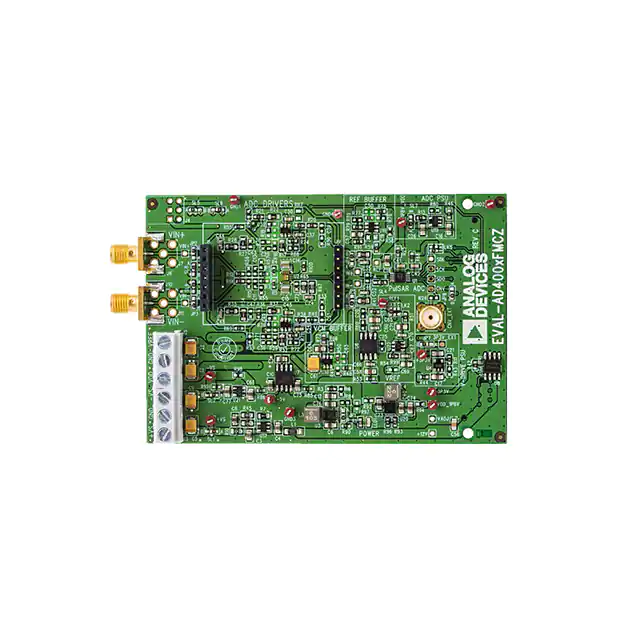
14981-055
EVALUATION BOARD PHOTOGRAPH
Figure 1. EVAL-AD400x-FMCZ
Rev. I | Page 4 of 30
�Easy to Use AD4000 Series 16-/18-/20-Bit Precision SAR ADCs User Guide
UG-1042
EVALUATION BOARD HARDWARE
12V
WALL WART
(OPTIONAL)
–VS
GND
POWER SUPPLY CIRCUITRY
ADP7118, ADP2370, ADM660, ADP7182
+VS
+7V/+5V/–2.5
+1.8V
+7V
+3.3V
(OPTIONAL)
12V
12V
USB PORT
ADR4550
5V
VDD
GND
POWER
SUPPLY
CIRCUITRY
VCM
VREF
ADA4807-1
ADA4807-1
ADA4807-1
+7V
VDD REF VIO
AD4000/ SDI
VIN+
IN+
ADA4807-1
IN–
VIN–
A B
AD4001/
AD4002/
AD4003/
AD4020
SCK
SDO
ADSP-BF527
CNV
SPARTAN-6
FPGA
XC6SLX25
SPI
INTERFACE
GND
–2.5V
EASY TO USE AD4000 SERIES 16-BIT/18-BIT/20-BIT
PRECISION SAR ADCs EVALUATION BOARD
SDP-H1
14981-001
–2.5V
+7V
160-PIN
FMC CONNECTOR
Figure 2. Simplified Evaluation Board Block Diagram
SETTING UP THE EVALUATION BOARD
Figure 2 shows the simplified evaluation board block diagram.
Figure 24 shows the evaluation board schematic. The board
consists of the ADC, U1, with a reference, U6 (ADR4550), and
ADC drivers, U12 and U14, the ADA4807-1 for the AD4001/
AD4002/AD4003/AD4020, and the ADA4805-1 for the
AD4000 (see Table 6). The user also has an option to populate
U2 with a low power, fully differential ADC driver, such as the
ADA4940-1, when evaluating the AD4001/AD4003/AD4020.
The evaluation board is a flexible design that enables the user to
select components in addition to operating from an adjustable
bench top power supply.
Each supply is decoupled where it enters the board and at each
device. A single ground plane is used on this board to minimize
the effect of high frequency noise interference.
In addition, the board can be powered from a benchtop power
supply. The screw terminals, J2 and J3, are provided for this
function. When bench power is used, the on-board power
supplies are no longer required. The solder links also must be
changed as follows: SL1 = SL2 = SL5 = SL6 = SL7 = SL8 = SL9 = B.
Table 1. Power Supplies Provided on the Board
Power Supply (V)
5, 7 (Default)1
−5, −2.5 (Default)1
Function
Positive rail
Negative rail
A sticker label included on the bottom side (not pictured) of the
EVAL-AD4000FMCZ/EVAL-AD4001FMCZ/EVALAD4002FMCZ/EVAL-AD4003FMCZ/EVAL-AD4020FMCZ
indicates evaluation board options. For example, the EVALAD4020FMCZ evaluation board includes a sticker labeled
EVAL-AD4020FMCZ.
1.8
3.3
ADC power
VDRIVE (digital power)
POWER SUPPLIES
An external 5 V reference (U6, ADR4550) is used by default to
supply the ADCs directly. The user can also use one of the 2.5 V,
3.3 V, and 4.096 V references by changing the on-board reference
device U6 (ADR4525/ADR4533/ADR4540). There is an option to
use a lower power reference, U22 (ADR3450). Note that the
ADR3450 cannot accept input voltages beyond 5.5 V. The
ADA4807-1 is used as a reference buffer (U16) and common-mode
buffer (U18) by default. However, U16 can also be replaced by
the AD8031 if required without compromising the
performance.
Identifying the Evaluation Board
The system demonstration platform (SDP-H1) board supplies
12 V to power the necessary rails for the EVAL-AD400x-FMCZ
evaluation boards.
The 7 V amplifier positive rail (+VS) is generated from U17
(ADP7118). The −2.5 V negative amplifier rail (−VS) is
generated by a combination of U3 (ADP2370), U7 (ADM660),
and U21 (ADP7182).
1
Components Used
ADP7118
ADP2370, ADM660,
ADP7182
ADP7118, ADP5300
ADP7118
See Table 2.
REFERENCE, REFERENCE BUFFER, AND COMMONMODE BUFFER
Rev. I | Page 5 of 30
�UG-1042
Easy to Use AD4000 Series 16-/18-/20-Bit Precision SAR ADCs User Guide
SDP-H1 CONTROLLER BOARD
SOLDER LINKS
The evaluation board uses a serial port interface (SPI) and is
connected to the system demonstration platform (SDP-H1)
controller board. The SDP-H1 board requires power from a 12 V
wall adapter (included with the SDP-H1). The SDP-H1 has a
Xilinx® Spartan 6 and an ADSP-BF527 processor with connectivity
to the PC through a USB 2.0 high speed port. The SDP-H1
allows the configuration and capture of data on the evaluation
boards from the PC via USB.
The three solder link options on the evaluation board are
configured depending on the generic of the ADC on the
specific evaluation board, as described in Table 3.
The evaluation board supports any amplifier mezzanine card
(AMC). Insert this add on card on the 7-pin headers. Figure 3
shows the AMC mounted on the evaluation board. The AMC
ADC driver settings are required to use this option, described
in Table 4.
14981-103
The SDP-H1 has an FMC LPC connector with full differential low
voltage differential signaling (LVDS) and singled-ended low voltage
complementary metal-oxide semiconductor (LVCMOS) support.
The SDP-H1 also has a 120-pin connector that exposes the
Blackfin® processor peripherals. This connector provides a
configurable serial, parallel I2C and SPI, and general-purpose
input/output (GPIO) communications lines to the attached
daughter board.
Figure 3. AMC Installed on the EVAL-AD400x-FMCZ
Table 2. Jumper Detail with Factory Default Setting
Link
SL1
SL2
SL5
SL6
SL7
LK2
LK51
JP1
Default Position
A
A
A
A
A
A
B
B
Function
+VS
−VS
+VS
−VS
VDD for ADC
VREF
SDI
FSEL (U3)
JP2
JP3
JP4
JP5
JP7
JP8
B
B
B
B
B
B
ADC drivers
ADC drivers
ADC drivers
ADC drivers
V_DRIVE
Stop (U20)
1
Comments
Change to Position B if using bench supplies
Change to Position B if using bench supplies
Change to Position B if using bench supplies
Change to Position B if using bench supplies
Change to Position B if using bench supplies
Change to Position B if using the ADR3450
Change to Position A if using connecting SDI to the VIO voltage (V_DRIVE)1
Change to Position A if selecting a 600 kHz switching frequency for the
ADP2370 (U3)
Change to Position A if using the ADA4940-1 fully differential ADC
Change to Position A if using the ADA4940-1 fully differential ADC
Change to Position A if using the ADA4940-1 fully differential ADC
Change to Position A if using the ADA4940-1 fully differential ADC
Change to Position A if using external 3.3 V for V_DRIVE (VIO voltage)
Change to Position A if synchronizing ADP5300 (U20) STOP input with
CNV_FMC from SDP-H1 connector
Setting LK5 to Position A prevents access to the configuration register of the connected device and does not allow features including turbo mode, high-Z mode, and
so on, to be enabled.
Table 3. Jumpers Specific to 10-Lead Precision ADCs
Link
SL4
SL4
Default Position
A
B
Configuration
Differential input
Single-ended or pseudo differential
Rev. I | Page 6 of 30
Generic
AD4001, AD4003, AD4020
AD4000, AD4002
�Easy to Use AD4000 Series 16-/18-/20-Bit Precision SAR ADCs User Guide
UG-1042
Table 4. EVAL-AD400x-FMCZ Configuration Settings for Amplifier Mezzanine Card ADC Driver
Component
SL8
SL9
JP4, JP5
Default Position/Values
A
A
B
Function
−VS
+VS
ADC driver outputs
R20, R40
0Ω
ADC driver outputs
R69, R95
0Ω
ADC driver inputs
R28, R35
590 Ω
Provides dc common-mode
voltage to ADC driver inputs
ANALOG INPUTS
The analog inputs to the evaluation board are SMA connectors,
J6 and J10. These inputs are buffered with dedicated amplifier
circuitry (U12 and U14), as shown in Figure 26. The circuit
allows different configurations, input range scaling, filtering,
addition of a dc component, and use of different op amp and
supplies. The analog input amplifiers are set as unity-gain
buffers at the factory.
The optional fully differential amplifier (FDA) can be used with the
fully differential AD4000 devices on the EVAL-AD4001FMCZ,
EVAL-AD4003FMCZ, and EVAL-AD4020FMCZ boards. Table 2
lists the necessary jumper positions for using the FDA (U2).
The AD4000 family devices require the inputs to be biased at
midscale. The default configuration also sets both U12 and U14
at midscale, generated from a buffered reference voltage divider
(VCM). The noninverting inputs of both U12 and U14 are
connected to the 590 Ω resistor dividers by default. These resistor
Comments
Change to Position B if using bench supplies for AMC power
Change to Position B if using bench supplies for AMC power
Must be set to Position B to connect the ADC inputs to the AMC
outputs
Must not be installed in order to disconnect the on-board ADC
driver outputs (U12 and U14)
Must not be installed in order to disconnect the on-board ADC
driver inputs (U12 and U14)
Must not be installed in order to disconnect the dc common-mode
voltage from the on-board ADC driver inputs (U12 and U14)
dividers, R27, R28, R34, and R35, divide the reference voltage in
half. The 590 Ω resistor dividers must be taken into account when
interfacing with an external source via J6 and J10. The FDA
(U2) outputs are biased to midscale with a 10 kΩ resistor
divider (R65 and R67).
The EVAL-AD400x-FMCZ evaluation boards are factory
configured to provide the appropriate input signal type, singleended or fully differential, with the SL4 link. See Table 2 and
Figure 26 for more information.
To evaluate dynamic performance, a fast Fourier transform
(FFT) test can be performed by applying a very low distortion
ac source.
For low frequency testing, the audio precision source (such as the
SYS-2700 series) can be used directly because the outputs on these
are isolated. Set the outputs for balanced and floating ground.
Different precision sources can be used with additional filtering.
Rev. I | Page 7 of 30
�UG-1042
Easy to Use AD4000 Series 16-/18-/20-Bit Precision SAR ADCs User Guide
GETTING STARTED
The EVAL-AD400x-FMCZ evaluation boards can be controlled
with the AD40XX Evaluation Software Installer. The following
sections provide instructions for installing the supporting
software and an overview for connecting the hardware to the PC.
4.
Choose the installation directory and click Next. The default
location is C:\Program Files (x86)\Analog Devices\.
SOFTWARE INSTALLATION PROCEDURES
The AD40XX Evaluation Software Installer installs the
AD40XX Evaluation Software Installer and accompanying
drivers for the SDP-H1 board. Install this software installer
package before connecting the SDP-H1 board to the PC USB port
to ensure that the SDP-H1 board is recognized when it connects
to the PC.
Installing the AD40XX Evaluation Software Installer
Figure 5. Destination Directory Window
5.
Installing the AD40XX Evaluation Software Installer
requires users to accept the license agreement shown in
Figure 6. Read the agreement before clicking Next to
proceed.
14981-106
2.
3.
Start the Windows® operating system and download the
software from the EVAL-AD400x-FMCZ product page.
Unzip the downloaded file. Run the setup.exe file.
Begin installing the evaluation software by clicking the
setup.exe file. The software installation window opens as
shown in Figure 4.
14981-104
1.
14981-105
To install the AD40XX Evaluation Software Installer, adhere to
the following steps:
Figure 6. License Agreement Window
Figure 4. AD40XX Evaluation Software Install Window
Rev. I | Page 8 of 30
�Easy to Use AD4000 Series 16-/18-/20-Bit Precision SAR ADCs User Guide
The window shown in Figure 7 provides a summary of the
software installation. Click Next to install the software
listed in the window.
Installing the SDP-H1 Board Drivers
The AD40XX Evaluation Software Installer uses the ADI SDP
drivers (Version 2.3.0.207) to interface with the SDP-H1 controller
board. Following the successful software installation, the installer
automatically begins installing the ADI SDP drivers (indicated by
the pop-up shown in Figure 10).
14981-008
6.
UG-1042
Figure 10. SDP-H1 Driver Installation
The ADI SDP Drivers 2.3.0.207 Setup wizard opens the
window, as shown in Figure 11. Click Next to install the
SDP-H1 drivers.
14981-107
1.
Figure 7. Start Installation Window
A pop-up window opens and displays a bar showing the
installation progress, as shown in Figure 8.
14981-111
7.
Figure 11. ADI SDP Drivers 2.3.0.207 Setup Window
14981-108
2.
Installing the ADI SDP Drivers 2.3.0.207 requires the user
to accept the license agreement that appears in Figure 12.
Read the agreement before clicking I Agree to proceed.
Figure 8. Overall Progress
14981-112
Click Next to complete the installation and launch the
SDP-H1 driver installation, as shown in Figure 9.
Figure 12. ADI SDP Drivers (v2.3.0.207) License Agreement Window
14981-109
8.
Figure 9. Installation Complete Window
Rev. I | Page 9 of 30
�UG-1042
Choose the destination folder for the ADI SDP drivers and
click Install. The default folder is shown in Figure 13.
5.
Click the Close button shown in Figure 15 when the
installation is complete.
14981-115
14981-113
3.
Easy to Use AD4000 Series 16-/18-/20-Bit Precision SAR ADCs User Guide
Figure 13. Choose Install Location
When plugging in the SDP-H1 board via the provided USB cable,
allow the Found New Hardware Wizard to run. Check that the
drivers are installed and the SDP-H1 board are connected properly
by checking the Device Manager of the PC. If the drivers and
board are connected, Analog Devices System Development
Platform (32MB) appears under ADI Development Tools (see
Figure 16).
Figure 14. Installing
Rev. I | Page 10 of 30
14981-013
The installation begins, and a progress bar shown in Figure 14
is displayed.
14981-114
4.
Figure 15. Installation Complete
Figure 16. Device Manager Menu
�Easy to Use AD4000 Series 16-/18-/20-Bit Precision SAR ADCs User Guide
UG-1042
Uninstalling the Software
Connecting the Evaluation Hardware to a PC
To uninstall the AD40XX Evaluation Software Installer, take the
following steps:
To connect the EVAL-AD400x-FMCZ evaluation board and
SDP-H1 board to a PC:
1.
1.
2.
Launch the uninstall wizard by navigating to Start >
Control Panel > Programs and Features > AD40XX
Customer Evaluation Software to open a window with the
Uninstall button.
Click Yes in the confirmation window that appears.
3.
To uninstall the SDP drivers, adhere to the following steps:
1.
2.
2.
Before connecting power, connect the FMC connector of
the EVAL-AD400x-FMCZ evaluation board (J5) to the
FMC connector on the SDP-H1 board (J4).
Power the SDP-H1 with the appropriate supply, as
described in the Power Supplies section.
Connect the SDP-H1 to the PC with the USB cable.
Verifying Hardware Connection
Launch the uninstall wizard by navigating to Start >
Control Panel > Programs and Features > ADI SDP
Drivers 2.3.0.207 to open a window with the Uninstall
button.
Click Yes in the confirmation window that appears.
To verify the AD4000 family evaluation board is properly
connected to the PC, take the following steps:
1.
Allow the Found New Hardware Wizard to finish running
after the SDP-H1 board is connected to the PC via the USB
cable. Choose the automatically search for the appropriate
drivers option for the SDP drivers if prompted.
2.
Verify the hardware to PC connection by navigating to the
Device Manager via the Control Panel. If the hardware is
properly connected, Analog Devices SDP-H1 appears
under ADI Development Tools.
EVALUATION HARDWARE SETUP PROCEDURES
The EVAL-AD400x-FMCZ evaluation boards connect to the
SDP-H1 via the FMC connector (J5). The SDP-H1 is the
controller board and functions as the communication link between
the PC and connected EVAL-AD400x-FMCZ evaluation board.
Rev. I | Page 11 of 30
�UG-1042
Easy to Use AD4000 Series 16-/18-/20-Bit Precision SAR ADCs User Guide
SOFTWARE OPERATION
1
3
2
4
5
7
11
8
9
10
12
13
14
14981-117
6
Figure 17. AD40XX Evaluation Software Front Panel (Configure Tab View)
RUNNING THE EVALUATION SOFTWARE
After installing the AD40XX Evaluation Software Installer (see
the Software Installation Procedures section), run the software
with either of the following methods:
•
Navigate to the destination folder of the AD40XX
Evaluation Software Installer selected during the
installation procedure and run the EVAL-AD40xx.exe file.
Click Start > All Programs > Analog Devices > AD40XX
Evaluation Software > AD40xx Evaluation Software.
14981-118
•
Figure 18. Connectivity Error Dialog Box
ESTABLISHING HARDWARE CONNECTION
After the AD40XX Evaluation Software Installer initializes, the
software front panel appears, and the software automatically
connects to any EVAL-AD400x-FMCZ evaluation board
connected to the PC. The detected evaluation board is displayed
in the Eval Board Connected indicator on the front panel (see
Label 7 in Figure 17).
If the software does not detect a valid EVAL-AD400x-FMCZ
evaluation board, a connectivity error dialog box appears (see
Figure 18). Clicking the Rescan button instructs the software to
try to detect the hardware again. Clicking the Offline Mode
button causes the software to boot in offline mode. See the
Saving and Loading Sessions section for the functions provided
in offline mode.
OVERVIEW OF THE FRONT PANEL
The AD40XX Evaluation Software Installer front panel is
shown in Figure 17. The following sections describe the various
software controls accessible on the front panel.
File Menu
The File menu (Label 1 in Figure 17) provides the following
options:
•
Rev. I | Page 12 of 30
Save Captured Data (Ctrl + S): saves the current AD40XX
Evaluation Software Installer session in a .csv file. The user
is prompted to either choose or enter the path of the file in
the Save As dialog box. This saved file can be loaded by the
software at a future time to display previously captured data.
�Easy to Use AD4000 Series 16-/18-/20-Bit Precision SAR ADCs User Guide
•
•
•
•
Load Captured Data (Ctrl + O): opens the Load File dialog
box and the user is prompted to load the previously saved
evaluation software session files (.csv).
Take Screenshot: saves the current front panel display as
an image file (.jpg). The user is prompted to either choose
or enter the path of the file in a Save As dialog box.
Print Screenshot: sends a screenshot of the current front
panel display directly to the default printer identified by
the operating system for printing.
Exit: closes the AD40XX Evaluation Software Installer
front panel and exits the software.
Edit Menu
•
Status Bar
The status bar (Label 6 in Figure 17) displays information about
the current process being completed by the AD40XX Evaluation
Software Installer. The Status Bar includes a Busy indicator, which
displays if the software is busy performing a task such as
performing conversions, analyzing results, and so on.
CONFIGURE TAB
Figure 17 shows the Configure tab view. The Configure tab
provides controls for configuring the connected AD4000 family
device and software settings. The Configure tab view contains
the following controls and indicators:
•
The Edit (Label 1 in Figure 17) menu provides the following
option:
•
Reinitialize Default Values: resets a subset of the
AD40XX Evaluation Software Installer front panel controls
to the default state.
Help Menu
The Help menu (Label 1 in Figure 17) provides the following
options:
•
•
•
•
•
Analog Devices Website: opens the Analog Devices webpage
(www.analog.com) in the default browser of the PC.
AD4000 Evaluation Hardware Info: opens the AD4000
family evaluation board EVAL-AD400x-FMCZ product
page in the default browser of the PC.
Context Help (Ctrl + H): displays a context help dialog
box, which displays information about the various software
controls when the mouse hovers over them.
About (Ctrl + A): displays version and copyright information
of the AD40XX Evaluation Software Installer in a dialog box.
Display Tabs
The following five tabs are located at the top of the front panel
(Label 2 in Figure 17): Configure, Waveform, Histogram, FFT,
and Summary. These tabs select various front panel views.
•
•
Single Capture Button
Click Single Capture (Label 3 in Figure 17) to perform a single
set of conversions. The number of conversions performed is set
with the Samples dropdown list, which is located to the left of
the Single Capture control.
Continuous Capture Button
Click Continuous Capture (Label 4 in Figure 17) to perform
repeated sets of conversions. The number of conversions
performed per set is set with the Samples dropdown list.
•
Samples Dropdown List
The Samples dropdown list (Label 5 in Figure 17) sets the
number of conversions that are performed when Single Capture is
clicked. The button also sets the number of conversions per set
when Continuous Capture is clicked.
UG-1042
•
Rev. I | Page 13 of 30
Eval Board Connected (Label 7 in Figure 17): indicates that
the EVAL-AD400x-FMCZ board is connected to the software.
Reference Voltage (VREF) (Label 8 in Figure 17): sets the
VREF used in data analysis such as when calculating LSB
Size (see Label 2 in Figure 19), or measured voltage in the
waveform graph (see the Waveform Tab View section. This
control must be set to match the VREF used on the
connected AD4000 family evaluation board.
Oversampling Ratio (Label 9 in Figure 17): sets the
oversampling ratio applied to the captured data. After this
control is set to any value other than None, the software
sums up the consecutive conversion results together to
increase effective resolution. The number of conversions
summed together is set by the Oversampling Ratio control.
Throughput (kSPS) (Label 10 in Figure 17): sets the
throughput of the connected AD4000 family device. The
maximum value of this control is automatically set to reflect
the maximum achievable throughput of the connected
device, given the state of the Status Bits and Turbo Mode
controls. See the relevant AD4000 family device data sheet
for more information on maximum achievable throughput.
Device Config Settings (Label 11 in Figure 17): configures
the connected AD4000 family device user configuration
register settings. See the relevant AD4000 family device data
sheet for a detailed description of the user configuration
register and the device features.
• Status Bits: enables or disables the status bits for the
connected device.
• Span Compression: enables or disables span
compression for the connected device.
• High-Z Mode: enables or disables high-Z mode.
• Turbo Mode: enables or disables turbo mode for the
connected device.
Read Register (Label 12 in Figure 17): reads the AD4000
family device user register. When Read Register is clicked,
the contents of the connected AD4000 family device register
are read to update the Device Config Settings items
accordingly.
Device configuration settings display (Label 13 in
Figure 17): displays the status of the user register when
Read Register is clicked. Each of the following indicators
displays the state of the corresponding settings:
�UG-1042
Easy to Use AD4000 Series 16-/18-/20-Bit Precision SAR ADCs User Guide
•
•
Status Bits, Span Compression, High-Z Mode, and
Turbo Mode status indicators indicate whether the
corresponding AD4000 family device are reported as
enabled or disabled in the user configuration register
of the connected AD4000 family device.
• Overvoltage Clamp Flag: indicates the status of the OV
clamp flag in the user configuration register of the
connected device. When this indicator is red, the OV flag
is low, indicating the presence of an overvoltage event.
Status Bits Indicators (Label 14 in Figure 17): displays the
configuration settings of the device as indicated by the
status bits. The status bits are enabled with the Status Bits
control in the Device Config Settings pane (Label 11 in
Figure 17). The Status Bits Indicators are only updated
after conversions are performed with the Single Capture
or Continuous Capture controls when the status bits are
enabled on the connected AD4000 family device. The
Rev. I | Page 14 of 30
status bit functionality is described in the relevant AD4000
family device data sheet.
• The Span Compression, High-Z Mode, and Turbo
Mode status indicators indicate whether features of
the corresponding AD4000 family device is reported
as enabled or disabled by the status bits of the
connected AD4000 family device.
• Overvoltage Clamp Flag: displays whether the OV
clamp flag in the status bits indicated an overvoltage
event in any of the conversions in the most recently
displayed results. When this indicator is red, the OV
flag is low, indicating the presence of an overvoltage
event. See the AD4000 family data sheets for more
details on the OV clamp flag.
�Easy to Use AD4000 Series 16-/18-/20-Bit Precision SAR ADCs User Guide
UG-1042
WAVEFORM TAB VIEW
1
3
14981-119
2
Figure 19. Waveform Tab View
•
Figure 19 shows the Waveform tab view. The Waveform tab
view shows the time domain representation of the conversion
results from the connected AD4000 family device, as well as
several analysis items. The Waveform tab view contains the
following controls and indicators:
•
•
Waveform graph (Label 1 in Figure 19): displays the time
domain plot of the most recently captured or loaded
conversion results. The scale and range of the waveform
graph can be set in the Waveform Analysis box by double
clicking on the Minimum Value and Maximum Value
fields and entering the desired values. The waveform graph
also includes viewing tools that are described in Table 5.
Waveform Analysis (Label 2 in Figure 19): shows the
following analysis items for the currently displayed data.
• Number of Samples: displays the number of captured
samples in the data displayed in the waveform graph.
The displayed value factors in the oversampling ratio
that is set with the OSR control.
• Pk-Pk Amplitude: displays the peak-to-peak
amplitude of the captured data (the difference
between the Maximum Value and the Minimum
Value).
• Maximum Value: displays the maximum value
measured in the captured data.
• Minimum Value: displays the minimum value
measured in the captured data.
• OSR: displays the oversampling ratio applied to the
captured data. The OSR can be changed using the
Oversampling Ratio control in the Configure tab view.
•
Rev. I | Page 15 of 30
LSB Size: displays the effective size (in μV) of each
LSB given the resolution of the connected AD4000
family device, the Reference Voltage (VREF), and the
Oversampling Ratio values selected in the Configure
tab view.
• Mean: displays the arithmetic mean of the captured data.
• Standard Deviation: displays the standard deviation
of the captured data.
Graph Configuration pane (Label 3 in Figure 19): sets the
following waveform graph axis properties.
• X units: sets the x-axis units of the waveform graph.
The x-axis units can be either set to samples or seconds.
The time step size, when Seconds is selected, is calculated
from the selected Throughput and Oversampling
Ratio controls in the Configure tab view.
• Y units: sets the y-axis units of the waveform graph.
The y-axis units can be either set to codes or volts.
The voltage values, displayed when Volts is selected, is
calculated from the LSB Size in the Waveform
Analysis items.
• X-axis: autoscale: sets whether the x-axis range of the
waveform graph autoscales as new data is plotted or
remains at a fixed scale.
• Y-axis: autoscale: sets whether the y-axis range of the
waveform graph autoscales or remains at a fixed scale
as new data is plotted.
�UG-1042
Easy to Use AD4000 Series 16-/18-/20-Bit Precision SAR ADCs User Guide
HISTOGRAM TAB VIEW
1
14981-120
2
Figure 20. Histogram Tab View
Figure 20 shows the Histogram tab view. The Histogram tab is
useful for performing statistical analysis of the AD4000 family
device conversion results, especially when measuring dc signals.
The histogram graph shows the distribution of the conversion
results as well as various statistical analysis items. The Histogram
tab contains the following controls and indicators:
•
•
Histogram graph (Label 1 in Figure 20): displays histogram of
the most recently captured or loaded conversion results.
The scale and range of the histogram graph can be set by
double-clicking on the minimum and maximum axis
values and entering the desired values. The histogram
graph also includes viewing tools, described in Table 5.
Histogram Analysis (Label 2 in Figure 20): shows the
following analysis items for the currently displayed data.
• Number of Samples: displays the number of captured
samples in the data displayed in the histogram graph.
The displayed value factors in the oversampling ratio
shown in the OSR indicator.
Rev. I | Page 16 of 30
•
•
•
•
•
•
•
Pk-Pk Amplitude: displays the peak-to-peak
amplitude of the captured data (the difference between
the Maximum Value and the Minimum Value).
Maximum Value: displays the maximum value
measured in the captured data.
Minimum Value: displays the minimum value
measured in the captured data.
OSR: displays the oversampling ratio applied to the
captured data. The OSR can be changed using the
Oversampling Ratio control in the Configure tab view.
LSB Size: displays the effective size (in μV) of each LSB
given the resolution of the connected AD4000 family
device, and the Reference Voltage (VREF) and
Oversampling Ratio values selected in the Configure tab.
Mean: displays the arithmetic mean of the captured data.
Standard Deviation: displays the standard deviation
of the captured data.
�Easy to Use AD4000 Series 16-/18-/20-Bit Precision SAR ADCs User Guide
UG-1042
FFT TAB VIEW
1
4
3
14981-121
2
Figure 21. FFT Tab View
•
Figure 21 shows the FFT tab view. The FFT tab displays the
calculated FFT representation of the conversions results from the
connected AD4000 family device and common ac performance
metrics. The FFT tab contains the following controls and
indicators:
•
•
FFT graph (Label 1 in Figure 21): displays an FFT of the
most recently captured or loaded conversion results. Set
the scale and range of the FFT graph by double clicking on
the minimum and maximum values along the x-axis and yaxis and entering the desired values. The FFT graph also
includes viewing tools that described in Table 5.
FFT Analysis (Label 2 in Figure 21): displays common ac
performance metrics of the captured data. Results are
calculated from the FFT spectrum, typically ignoring the
first six frequency bins.
• Throughput: displays the effective throughput (sample
rate) of the captured data. The displayed value factors in
the oversampling ratio displayed in the OSR indicator.
• Bin Width: displays the size of the frequency bins in the
FFT graph x-axis. The bin width is a function of both the
Throughput (kSPS) control (Label 10 in Figure 17) and
the number of samples in the captured data.
• OSR: displays the oversampling ratio applied to the
captured data. The OSR can be changed using the
Oversampling Ratio control in the Configure tab.
• LSB Size: displays the effective size (in μV) of each
LSB. The LSB size is a function of the resolution of the
connected AD4000 family device, the Reference
Voltage (VREF), and the Oversampling Ratio values
selected in the Configure tab view.
• Dynamic Range: displays the calculated dynamic range.
• SNR: displays the calculated signal-to-noise ratio (SNR).
•
•
Rev. I | Page 17 of 30
THD: displays calculated total harmonic distortion
(THD), up to the fifth harmonic.
• SINAD: displays the calculated single-to-noise and
distortion ratio (SINAD).
• SFDR: displays the calculated spurious-free dynamic
range (SFDR).
• Fund. Frequency: displays the frequency identified as
fundamental, the frequency bin with the largest signal.
• Fund. Amplitude: displays amplitude of the fundamental
frequency, the frequency bin with the largest signal.
• RMS Noise: displays the measured rms voltage noise.
• Avg. Noise Floor: displays the average amplitude of noise
frequency bins, more specifically, bins not identified as
fundamental or harmonic.
Show Harmonic Content: contains Frequency and
Amplitude information for the fundamental and harmonic
tones identified in the FFT. These displays are only visible
when toggled by the Show Harmonic Content control and
are not displayed in Figure 21.
• Frequency: frequency bins identified as fundamental and
harmonic.
• Amplitude: amplitude of the fundamental and harmonic
frequencies.
Graph Configuration: sets the following FFT graph axis
properties.
• X-axis: autoscale: sets whether the FFT graph x-axis range
autoscales as new data is plotted or remains at a fixed scale.
• Y-axis: autoscale: sets whether the FFT graph y-axis range
autoscales as new data is plotted or remains at a fixed
scale.
• X-axis scale: sets whether the FFT graph x-axis scaling
is linear or logarithmic.
�UG-1042
Easy to Use AD4000 Series 16-/18-/20-Bit Precision SAR ADCs User Guide
SUMMARY TAB VIEW
1
3
4
14981-122
2
Figure 22. AD40XX Evaluation Software Summary Tab View
Figure 22 shows the Summary tab view. The Summary tab
simultaneously displays the waveform, histogram, and FFT
graphs and analysis for the AD4000 family device conversion
results on the screen. The Summary tab contains the following
controls and indicators:
•
•
•
•
•
•
Waveform graph (Label 1 in Figure 22): displays the time
domain plot of the most recently captured or loaded
conversion results. The scale and range of the waveform
graph can be set by double-clicking on the minimum and
maximum axis values along the x-axis and y-axis and
entering the desired values. The waveform graph also
includes viewing tools that are described in Table 5.
Histogram graph (Label 2 in Figure 22): displays the
histogram of the most recently captured or loaded conversion
results. The scale and range of the histogram graph can be
set by double-clicking on the minimum and maximum
values along the x-axis and y-axis and entering the desired
values. The histogram graph also includes viewing tools
that are described in Table 5.
FFT graph (Label 3 in Figure 22): displays an FFT of the
most recently captured or loaded conversion results. The
scale and range of the FFT graph can be set by double
clicking on the minimum and maximum axis values and
entering the desired values. The FFT graph also includes
viewing tools that are described in Table 5.
Analysis Summary (Label 4 in Figure 22): shows the
following analysis items for the currently displayed data.
• Pk-Pk Amp: displays the peak-to-peak amplitude of
the captured data.
• Mean: displays the arithmetic mean of the captured data.
• Standard Deviation: displays the standard deviation
of the captured data.
Rev. I | Page 18 of 30
•
•
•
•
•
•
•
Fund. Freq.: displays frequency identified as the
fundamental (the frequency bin with the largest signal).
Fund. Amp.: displays the amplitude of the Fund. Freq.
RMS Noise: displays the measured rms voltage noise
of the captured data.
LSB Size: displays the effective size (in μV) of each
LSB. The LSB size is a function of the resolution of the
connected AD4000 family device, the Reference
Voltage (VREF), and Oversampling Ratio values
selected in the Configure tab.
Dynamic Range: displays the calculated dynamic
range of the captured data.
SNR: displays the calculated SNR of the captured data.
THD: displays the calculated THD of the captured
data (up to the fifth harmonic).
SINAD: displays the calculated SINAD of the
captured data.
SFDR: displays the calculated SFDR of the captured data.
�Easy to Use AD4000 Series 16-/18-/20-Bit Precision SAR ADCs User Guide
UG-1042
GRAPH VIEWING CONTROLS
The tools described in Table 5 allow users to control the
different chart displays within any of the chart panels in the
graphical user interface (GUI) tabs.
Table 5. GUI Tools
Symbol
Description
This tool controls the cursor, if present.
This tool zooms in and out of the data on the
graph.
This tool is used for panning.
SAVING AND LOADING SESSIONS
Clicking File > Save Captured Data or using the shortcut
Ctrl + S saves the capture data and relevant sampling parameters
for the currently displayed AD4000 family device in a .csv file.
These saved files can be loaded at a later time by clicking
File > Load Captured Data or using the shortcut Ctrl + O.
Upon loading these .csv files, the evaluation software displays
the data in the Waveform, Histogram, FFT, and Summary tabs.
The evaluation software also allows the user to export the raw
data of any of the graphs into a generic text file by right clicking
them and selecting Export > Export Data to Excel, as shown in
Figure 23. The exported data can be used for additional
postprocessing, but the generated text file cannot be loaded back
into the AD40XX Evaluation Software Installer.
14981-051
The AD40XX Evaluation Software Installer allow users to save
and load data to quickly recall previous results.
Figure 23. Export Raw Data
OFFLINE MODE
The AD40XX Evaluation Software Installer can be operated
without an accompanying EVAL-AD400x-FMCZ evaluation
board. If no EVAL-AD400x-FMCZ evaluation board is detected
when the software initializes, the dialog box in Figure 18 is
displayed. Clicking Offline Mode causes the evaluation
software to boot in offline mode.
In offline mode, new conversion results cannot be captured, but
previously saved AD40XX Evaluation Software Installer
sessions can be loaded to view previously captured data. See the
Saving and Loading Sessions section for instructions on loading
previously saved data.
Rev. I | Page 19 of 30
�UG-1042
Easy to Use AD4000 Series 16-/18-/20-Bit Precision SAR ADCs User Guide
TROUBLESHOOTING
SOFTWARE
HARDWARE
To troubleshoot the software, take the following steps:
To troubleshoot the hardware, take the following steps:
1.
1.
2.
3.
4.
5.
Always install the software before connecting the hardware to
the PC.
Always allow the install to fully complete (the software is a
two-part installation, the ADC evaluation software and the
SDP-H1 drivers). A restart is recommended after installation
is finished.
When the user first plugs in the SDP-H1 board via the
provided USB cable, allow the Found New Hardware
Wizard to run, which can take several seconds. However,
allow this to happen before starting the software.
If the EVAL-AD400x-FMCZ evaluation boards or SDP-H1
board are connected to the PC via the USB port but are not
being detected by the AD40XX Evaluation Software
Installer, ensure that the board is being recognized in the
Device Manager, as shown in Figure 16.
If connected to a slower USB port where the SDP-H1 cannot
read as quickly as it needs to, a timeout error can result. In
this case, it is advised not to read continuously, or
alternatively, to lower the number of samples taken.
2.
Rev. I | Page 20 of 30
If the software does not read back any data, do the following:
a. Check that the power is applied within the power
ranges described in the Power Supplies section.
b. Using a voltmeter, measure the voltage present at each
of the test points: +VS, −VS, 1P8V_VDD, VDD_1P8V,
+3P3V, +5V, and REF1, and common-mode voltages
(REF/2) at IN+ and IN− to ensure that they are accurate.
The SDP-H1 board LED1 must be illuminated.
c. Launch the software and read the data. If nothing
happens, exit the software.
d. Power down the board and relaunch the software.
e. If no data is read back, confirm that the ADC evaluation
board is connected to the SDP-H1 board and that the
board is being recognized in the Device Manager, as
shown in Figure 16.
When the user is working with the software in standalone/
offline mode (no hardware connected) and later chooses to
connect hardware, close and relaunch the software.
�Easy to Use AD4000 Series 16-/18-/20-Bit Precision SAR ADCs User Guide
UG-1042
14981-023
EVALUATION BOARD SCHEMATICS AND ARTWORK
Figure 24. EVAL-AD400x-FMCZ, Power Supplies
Rev. I | Page 21 of 30
�Easy to Use AD4000 Series 16-/18-/20-Bit Precision SAR ADCs User Guide
14981-024
UG-1042
Figure 25. EVAL-AD400x-FMCZ, Voltage Reference, Common-Mode and Reference Buffers
Rev. I | Page 22 of 30
�Easy to Use AD4000 Series 16-/18-/20-Bit Precision SAR ADCs User Guide
UG-1042
14981-025
Figure 26. EVAL-AD400x-FMCZ, ADC Drivers, and ADC
Rev. I | Page 23 of 30
�Easy to Use AD4000 Series 16-/18-/20-Bit Precision SAR ADCs User Guide
14981-026
UG-1042
Figure 27. EVAL-AD400x-FMCZ, EVAL-SDP-CH1Z Connector
Rev. I | Page 24 of 30
�UG-1042
14981-027
Easy to Use AD4000 Series 16-/18-/20-Bit Precision SAR ADCs User Guide
14981-028
Figure 28. EVAL-AD400x-FMCZ Silkscreen, Top Layer
Figure 29. EVAL-AD400x-FMCZ, Layer 1
Rev. I | Page 25 of 30
�14981-029
Easy to Use AD4000 Series 16-/18-/20-Bit Precision SAR ADCs User Guide
Figure 30. EVAL-AD400x-FMCZ, Layer 2
14981-030
UG-1042
Figure 31. EVAL-AD400x-FMCZ, Layer 3
Rev. I | Page 26 of 30
�UG-1042
14981-031
Easy to Use AD4000 Series 16-/18-/20-Bit Precision SAR ADCs User Guide
Figure 32. EVAL-AD400x-FMCZ, Layer 4
Rev. I | Page 27 of 30
�UG-1042
Easy to Use AD4000 Series 16-/18-/20-Bit Precision SAR ADCs User Guide
ORDERING INFORMATION
EVALUATION BOARD BILL OF MATERIALS
Table 6. Bill of Materials
Reference Designator
U1
U2
U3
U4
U6
U7
U8
U12, U14 (only for
AD4001/AD4002/
AD4003/AD4020)
U12, U14 (only for AD4000)
U16, U18
U17
U19
U20
U21
U22
C1, C2, C5, C9, C61
C3, C4, C16, C17, C21, C26
C6
C7, C10, C12, C18, C40, C68,
C73, C74, C75, C76, C77
C8, C57, C64, C69, C71
C14, C15
C24, C30, C37, C41, C42, C44,
C45, C48, C54, C60, C66, C67,
C70
C35, C52
C11, C13, C19, C20, C25, C29,
C32, C36, C38, C39, C43, C46,
C47, C49, C50, C51, C55, C63,
C72
C56
C58, C65
C186
L1
L3
L4
Description
16-/18-bit, 2 MSPS or 20-bit, 1.8 MSPS
precision SAR ADC in 10-lead mini small
outline package (MSOP)
Ultralow power, low distortion ADC
driver, 4 nV/√Hz
High voltage, 1.2 MHz/600 kHz, 800 mA,
low quiescent current buck regulator
Linear regulator, 3.3 V, ultralow noise,
complementary metal–oxide
semiconductor (CMOS)
Ultralow noise, high accuracy voltage
reference
CMOS, switched capacitor voltage
converter
IC EEPROM, 2 kb, 400 kHz, 8-lead small
outline integrated circuit (SOIC)
Low noise, high speed amplifier
Manufacturer
Analog Devices
Part Number
See Table 7
Stock Code
See Table 7
Analog Devices
ADA4940-1
Do not place
Analog Devices
ADP2370
ADP2370ACPZ-5.0-R7
Analog Devices
ADP7118
ADP7118AUJZ-3.3-R7
Analog Devices
ADR4550
ADR4550BRZ
Analog Devices
ADM660
ADM660ARZ
ST
M24C02-WMN6TP
Digi-Key 497-8552-1-ND
Analog Devices
ADA4807-1
ADA4807-1ARJZ
Low noise, high speed amplifier
Low noise, high speed amplifier
Linear regulator, 3.3 V, ultralow noise,
CMOS
Linear regulator, 1.8 V, ultralow noise,
CMOS
Ultralow power step-down regulator
–28 V, −200 mA, low noise, linear
regulator
Micropower, high accuracy, 5 V voltage
reference
10 µF, 20 V tantalum capacitor
2.2 µF, X7R, 16 V, 0805 capacitor,
multilayer ceramic capacitor (MLCC)
4.7 µF, 16 V, X7R, 0805 ceramic capacitor
10 µF, 16 V, 0805 capacitor
Analog Devices
Analog Devices
Analog Devices
ADA4805-1
ADA4807-1
ADP7118
ADA4805-1ARJZ
ADA4807-1ARJZ
ADP7118AUJZ-3.3-R7
Analog Devices
ADP7118
ADP7118AUJZ-1.8-R7
Analog Devices
Analog Devices
ADP5300
ADP7182
ADP5300ACPZ-1-R7
ADP7182AUJ-2.5-R7
Analog Devices
ADR3450
ADR3450ARJZ-R2
AVX
Murata
TAJB106K020RNJ
GRM21BR71C225KA12L
FEC 197427
FEC 1828829
Taiyo Yuden
Murata
EMK212B7475KG-T
GRM219R61C106KA73D
FEC 1853520
FEC 1845747
1 µF, X7R, 50 V, 0805 capacitor
100 nF, X7R, 25 V, 0805 capacitor
0.1 µF, X7R, 50 V ceramic capacitor
Murata
Murata
Murata
GRM21BR71H105KA12L
LLL216R71E104MA01L
GRM188R71H104KA93D
FEC 1735541
FEC 1294646
FEC 8820023
180 pF, 50 V, 0603, C0G/NP0 capacitor
YAGEO
(Phycomp)
Not applicable
CC0603JRNPO9BN181
FEC 3019494
Not applicable
Do not place
Murata
TDK
EPCOS
Wurth
GRM219R61E106KA12D
C2012X7R1H225K125AC
B37921C9104K60
742792141
FEC 2426961
FEC 2346945
Digi-Key 495-3265-1-ND
Wurth 742792141
Coilcraft
XAL4040-103ME
XAL4040-103ME
Coilcraft
XAL4020-222MEB
Coilcraft XAL4020222MEB
SMD capacitor
10 µF, X5R, 25 V, 0805, MLCC capacitor
2.2 µF, 50 V, 0805, X7R capacitor
SMD capacitor
1000 Ω at 100 MHz, 1206, WE-CBF SMD,
EMI suppression ferrite
10 µH, inductor, shielded power, XAL40
series
2.2 µH, inductor, shielded power, XAL40
series
Rev. I | Page 28 of 30
�Easy to Use AD4000 Series 16-/18-/20-Bit Precision SAR ADCs User Guide
UG-1042
Reference Designator
LED1
R1
R2
R3, R11, R12, R13, R14, R20, R21,
Description
LED, SMD, green
2.4 kΩ, 0.063 W, 1%, 0603 resistor
100 kΩ, 0.1 W, 1%, 0805 resistor
0 Ω, SMD resistor
Manufacturer
OSRAM
Multicomp
Multicomp
Multicomp
Part Number
LGQ971
MC0063W060312K4
MC01W08051100K
MC 0.063W 0603 0R
Stock Code
Digi-Key 475-1409-1-ND
FEC 9330879
FEC 9332405
FEC 9331662
R4, R5, R8, R9
R7
R10
R17, R22, R32, R37
R24, R41
R27, R28, R34, R35
R45, R65, R67
R93
R6, R15, R16, R18, R19, R26,
R29, R30, R31, R33, R39, R43,
R49, R54, R55, R56, R57, R58,
R60, R70, R71, R72, R76, R80,
R84, R87, R88, R89, R92, R94,
R97, R98, R101
J2, J3
J5
J6, J10
J8
J9
1 kΩ, 0.063 W, 1%, 0603 resistor
88.7 kΩ, 1%, 0805 resistor
1%, 0805 resistor
49.9 Ω, 0.1 W, 0.1%, 0805 resistor
200 Ω, 0.1 W, 1%, 0805 resistor
Thick film, chip, resistor
10 kΩ, 0.1 W, 1%, 0805 resistor
20 kΩ, 0.063 W, 1%, 0603 resistor
SMD resistor, 0603
Multicomp
Vishay Draloric
Multicomp
Panasonic
Multicomp
Vishay Draloric
Multicomp
Multicomp
Not applicable
MC0063W060311K
CRCW080588K7FKEA
MC01W08050R
RN73C2A49R9BTG
MC01W08051200R
CRCW0805590RFKEA
MC01W0805110K
MC0063W0603120K
Not applicable
FEC 9330380
FEC 2139026
FEC 9333681
FEC 1140694
FEC 9332758
FEC 1653021
FEC 9332391
FEC 9330771
Do not place
3-pin terminal block (5 mm pitch)
160-pin, 10 mm male, VITA 57 connector
Connector, jack end launch PC gold SMA
7-way, SSW, 2.54 mm, vertical socket
7-way, SIP, 2.54 mm, TH header
CamdenBoss
Samtec
Emerson
Samtec
Samtec
CTB5000/3
ASP-134604-01
142-0701-851
SSW-107-01-T-S
TLW-107-05-G-S
FEC 151790
Samtec ASP-134604-01
Digikey J658-ND
FEC 1803478
FEC 1668499
R23, R25, R36, R38, R40, R42,
R44, R46, R48, R50, R51, R52,
R53, R59, R66, R68, R69, R73,
R74, R75, R77, R78, R79, R85,
R86, R90, R91, R95, R96, R99,
R100
Table 7. Evaluation Board Models
Product
AD4000BRMZ
AD4001BRMZ
AD4002BRMZ
AD4003BRMZ
AD4020BRMZ
Ordering Model
EVAL-AD4000FMCZ
EVAL-AD4001FMCZ
EVAL-AD4002FMCZ
EVAL-AD4003FMCZ
EVAL-AD4020FMCZ
Maximum
Throughput
(MSPS)
2
2
2
2
1
Input Type
Pseudo differential
Fully differential
Pseudo differential
Fully differential
Fully differential
Sample Rate
(MSPS)
2
2
2
2
1.8
Rev. I | Page 29 of 30
Resolution (Bits)
16
16
18
18
20
Package Used on
Evaluation Board
10-lead MSOP
10-lead MSOP
10-lead MSOP
10-lead MSOP
10-lead MSOP
�UG-1042
Easy to Use AD4000 Series 16-/18-/20-Bit Precision SAR ADCs User Guide
NOTES
I2C refers to a communications protocol originally developed by Philips Semiconductors (now NXP Semiconductors).
ESD Caution
ESD (electrostatic discharge) sensitive device. Charged devices and circuit boards can discharge without detection. Although this product features patented or proprietary protection
circuitry, damage may occur on devices subjected to high energy ESD. Therefore, proper ESD precautions should be taken to avoid performance degradation or loss of functionality.
Legal Terms and Conditions
By using the evaluation board discussed herein (together with any tools, components documentation or support materials, the “Evaluation Board”), you are agreeing to be bound by the terms and conditions
set forth below (“Agreement”) unless you have purchased the Evaluation Board, in which case the Analog Devices Standard Terms and Conditions of Sale shall govern. Do not use the Evaluation Board until you
have read and agreed to the Agreement. Your use of the Evaluation Board shall signify your acceptance of the Agreement. This Agreement is made by and between you (“Customer”) and Analog Devices, Inc.
(“ADI”), with its principal place of business at One Technology Way, Norwood, MA 02062, USA. Subject to the terms and conditions of the Agreement, ADI hereby grants to Customer a free, limited, personal,
temporary, non-exclusive, non-sublicensable, non-transferable license to use the Evaluation Board FOR EVALUATION PURPOSES ONLY. Customer understands and agrees that the Evaluation Board is provided
for the sole and exclusive purpose referenced above, and agrees not to use the Evaluation Board for any other purpose. Furthermore, the license granted is expressly made subject to the following additional
limitations: Customer shall not (i) rent, lease, display, sell, transfer, assign, sublicense, or distribute the Evaluation Board; and (ii) permit any Third Party to access the Evaluation Board. As used herein, the term
“Third Party” includes any entity other than ADI, Customer, their employees, affiliates and in-house consultants. The Evaluation Board is NOT sold to Customer; all rights not expressly granted herein, including
ownership of the Evaluation Board, are reserved by ADI. CONFIDENTIALITY. This Agreement and the Evaluation Board shall all be considered the confidential and proprietary information of ADI. Customer may
not disclose or transfer any portion of the Evaluation Board to any other party for any reason. Upon discontinuation of use of the Evaluation Board or termination of this Agreement, Customer agrees to
promptly return the Evaluation Board to ADI. ADDITIONAL RESTRICTIONS. Customer may not disassemble, decompile or reverse engineer chips on the Evaluation Board. Customer shall inform ADI of any
occurred damages or any modifications or alterations it makes to the Evaluation Board, including but not limited to soldering or any other activity that affects the material content of the Evaluation Board.
Modifications to the Evaluation Board must comply with applicable law, including but not limited to the RoHS Directive. TERMINATION. ADI may terminate this Agreement at any time upon giving written
notice to Customer. Customer agrees to return to ADI the Evaluation Board at that time. LIMITATION OF LIABILITY. THE EVALUATION BOARD PROVIDED HEREUNDER IS PROVIDED “AS IS” AND ADI MAKES NO
WARRANTIES OR REPRESENTATIONS OF ANY KIND WITH RESPECT TO IT. ADI SPECIFICALLY DISCLAIMS ANY REPRESENTATIONS, ENDORSEMENTS, GUARANTEES, OR WARRANTIES, EXPRESS OR IMPLIED,
RELATED TO THE EVALUATION BOARD INCLUDING, BUT NOT LIMITED TO, THE IMPLIED WARRANTY OF MERCHANTABILITY, TITLE, FITNESS FOR A PARTICULAR PURPOSE OR NONINFRINGEMENT OF
INTELLECTUAL PROPERTY RIGHTS. IN NO EVENT WILL ADI AND ITS LICENSORS BE LIABLE FOR ANY INCIDENTAL, SPECIAL, INDIRECT, OR CONSEQUENTIAL DAMAGES RESULTING FROM CUSTOMER’S
POSSESSION OR USE OF THE EVALUATION BOARD, INCLUDING BUT NOT LIMITED TO LOST PROFITS, DELAY COSTS, LABOR COSTS OR LOSS OF GOODWILL. ADI’S TOTAL LIABILITY FROM ANY AND ALL CAUSES
SHALL BE LIMITED TO THE AMOUNT OF ONE HUNDRED US DOLLARS ($100.00). EXPORT. Customer agrees that it will not directly or indirectly export the Evaluation Board to another country, and that it will
comply with all applicable United States federal laws and regulations relating to exports. GOVERNING LAW. This Agreement shall be governed by and construed in accordance with the substantive laws of the
Commonwealth of Massachusetts (excluding conflict of law rules). Any legal action regarding this Agreement will be heard in the state or federal courts having jurisdiction in Suffolk County, Massachusetts, and
Customer hereby submits to the personal jurisdiction and venue of such courts. The United Nations Convention on Contracts for the International Sale of Goods shall not apply to this Agreement and is
expressly disclaimed.
©2016–2019 Analog Devices, Inc. All rights reserved. Trademarks and
registered trademarks are the property of their respective owners.
UG14981-0-11/19(I)
Rev. I | Page 30 of 30
�