AD7327/AD7328 Evaluation Board User Guide
UG-419
One Technology Way • P.O. Box 9106 • Norwood, MA 02062-9106, U.S.A. • Tel: 781.329.4700 • Fax: 781.461.3113 • www.analog.com
Evaluating the AD7327/AD7328
FEATURES
EVALUATION BOARD DESCRIPTION
Full-featured evaluation board for the AD7327/AD7328
PC control in conjunction with the system demonstration
platform (EVAL-SDP-CB1Z)
PC software for control and data analysis (time and
frequency domain)
Standalone capability
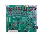
The EVAL-AD7327SDZ/EVAL-AD7328SDZ is a full-featured
evaluation board, designed to allow the user to easily evaluate
all features of the AD7327/AD7328. The evaluation board can
be controlled via the SDP connector (J2). The EVAL-SDP-CB1Z
board allows the evaluation board to be controlled via the USB
port of a PC using the AD7327/AD7328 evaluation software.
EVAL-AD7327SDZ/EVAL-AD7328SDZ KIT
CONTENTS
The EVAL-AD7327SDZ/EVAL-AD7328SDZ generates all required
power supplies on-board and supplies power to the EVAL-SDPCB1Z controller board.
EVAL-AD7327SDZ/EVAL-AD7328SDZ evaluation board
Evaluation software CD for the AD7327/AD7328
9 V mains power supply adapter
ADDITIONAL EQUIPMENT NEEDED
System demonstration platform (EVAL-SDP-CB1Z)
Precision analog signal source
SMB cables
USB cables
On-board components include the following:
•
•
•
•
•
•
•
•
AD8597: ultralow noise op amp
ADP1613: step-up PWM dc-to-dc switching converter
ADP3303-5: high accuracy anyCAP® 200 mA low dropout
linear regulator
ADP2301: 1.2 A, 20 V, 1.4 MHz nonsynchronous step-down
switching regulator
ADM1185: quad voltage monitor and sequencer
ADP190: logic controlled, high-side power switch
ADG3308: low voltage, 1.15 V to 5.5 V, 8-channel
bidirectional logic level translator
AD780: 5 V/3.0 V ultrahigh precision band gap voltage
reference
Various link options are described in the Evaluation Board
Hardware section.
PLEASE SEE THE LAST PAGE FOR AN IMPORTANT
WARNING AND LEGAL TERMS AND CONDITIONS.
Rev. 0 | Page 1 of 28
�UG-419
AD7327/AD7328 Evaluation Board User Guide
TABLE OF CONTENTS
Features .............................................................................................. 1
Evaluation Board Software ...............................................................9
EVAL-AD7327SDZ/EVAL-AD7328SDZ Kit Contents ............... 1
Software Installation .....................................................................9
Additional Equipment Needed ....................................................... 1
Launching the Software ............................................................. 11
Evaluation Board Description......................................................... 1
Software Operation .................................................................... 11
Revision History ............................................................................... 2
Description of User Software Panel ......................................... 12
Functional Block Diagram .............................................................. 3
Register Controls ........................................................................ 13
EVAL-AD7327SDZ/EVAL-AD7328SDZ Quick Start Guide ..... 4
Data Capture/WaveForm Tab ................................................... 14
Recommended Quick Start Guide ............................................. 4
AC Testing—Data Capture/Histogram Tab ............................ 15
Evaluation Board Hardware ............................................................ 5
DC Testing—Data Capture/Histogram Tab ........................... 15
AD7327 Device Description ....................................................... 5
AC Testing—Data Capture/FFT Tab ....................................... 16
AD7328 Device Description ....................................................... 5
Data Capture/Summary Tab ..................................................... 17
Hardware Link Options ............................................................... 5
Save File ....................................................................................... 18
Power Supplies .............................................................................. 7
Load File ...................................................................................... 18
Serial Interface .............................................................................. 8
Evaluation Board Schematics and Artwork ................................ 19
Analog Inputs ................................................................................ 8
Reference Options ........................................................................ 8
Sockets/Connectors...................................................................... 8
EVAL-AD7327SDZ/EVAL-AD7328SDZ Basic Hardware
Setup ............................................................................................... 8
REVISION HISTORY
10/12—Revision 0: Initial Version
Rev. 0 | Page 2 of 28
�AD7327/AD7328 Evaluation Board User Guide
UG-419
FUNCTIONAL BLOCK DIAGRAM
VCC
ON-BOARD
POWER SUPPLIES
GND
ADM1185
POWER
SEQUENCER
VSS
GND
OP AMP
SUPPLIES
VIN
GND
+
–
ADP1613
±15V
ADP2301
SDP 5V
ADP3303
+5V
ADP190
3.3V
VIN
7-9V
DC
INPUT
JACK
5V
VDD
BF527
DSP
VDRIVE
GND
VSS
VDD
VCC
VDRIVE
VIN0... 7IN7
AD7327/AD7328
BIPOLAR
INPUT SIGNALS
×8
INPUT
BUFFERS
×8
CS
SCLK
DIN
DOUT
ADG3308
LEVEL
SHIFTER
SERIAL
INTERFACE
REFIN/OUT
AD8597
AD780
EVAL-AD7327SDZ/EVAL-AD7328SDZ
Figure 1.
Rev. 0 | Page 3 of 28
EVAL-SDP-CB1Z
CONTROLLER
BOARD
10732-001
REF
�UG-419
AD7327/AD7328 Evaluation Board User Guide
EVAL-AD7327SDZ/EVAL-AD7328SDZ QUICK START GUIDE
4.
RECOMMENDED QUICK START GUIDE
To install the software, do the following:
2.
3.
Install the AD7327/AD7328 software from the enclosed CD.
When installing the software, ensure that the EVAL-SDPCB1Z board is disconnected from the USB port of the PC.
After installation, restart the PC.
Connect the EVAL-SDP-CB1Z board to the EVALAD7327SDZ/EVAL-AD7328SDZ board, as shown in
Figure 2.
Screw the EVAL-SDP-CB1Z board to the EVAL-AD7327SDZ/
EVAL-AD7328SDZ board together with the enclosed nylon
screw-nut set to ensure that the boards connect firmly
together.
5.
6.
9V PSU
EVAL-SDP-CB1Z
USB TO PC
Figure 2. Setting Up the EVAL-AD7327SDZ/EVAL-AD7328SDZ
Rev. 0 | Page 4 of 28
10732-002
1.
Connect the 9 V power supply adapter included in the kit
to the J702 connecter on the EVAL-AD7327SDZ/EVALAD7328SDZ board.
Connect the EVAL-SDP-CB1Z board to the PC via the
USB cable. For Windows® XP, searching for the EVALSDP-CB1Z drivers may be needed. If prompted by the
operating system, choose to automatically search for the
drivers for the EVAL-SDP-CB1Z board.
Launch the AD7327/AD7328 software from the Analog
Devices, Inc., subfolder in the All Programs menu.
�AD7327/AD7328 Evaluation Board User Guide
UG-419
EVALUATION BOARD HARDWARE
AD7327 DEVICE DESCRIPTION
The AD7327 is an 8-channel, 12-bit plus sign, successive
approximation analog-to-digital converter (ADC) designed
on the industrial CMOS (iCMOS) process. iCMOS is a process
that combines high voltage silicon with submicron CMOS and
complementary bipolar technologies. It enables the development
of a wide range of high performance analog ICs capable of 33 V
operation in a footprint that no previous generation of high voltage
parts could achieve. Unlike analog ICs using conventional CMOS
processes, iCMOS components can accept bipolar input signals
while providing increased performance, dramatically reduced
power consumption, and reduced package size.
The AD7327 can accept true bipolar analog input signals. The
AD7327 has four software-selectable input ranges: ±10 V, ±5 V,
±2.5 V, and 0 V to +10 V. Each analog input channel can be
independently programmed to one of the four input ranges.
The analog input channels on the AD7327 can be programmed
to be single-ended, true differential, or pseudo differential.
The ADC contains a 2.5 V internal reference. The AD7327 also
allows external reference operation. If a 3 V reference is applied
to the REFIN/OUT pin, the AD7327 can accept a true bipolar
±12 V analog input. Minimum ±12 V VDD and VSS supplies are
required for the ±12 V input range. The ADC has a high speed
serial interface that can operate at throughput rates up to 500 kSPS.
AD7328 DEVICE DESCRIPTION
The AD7328 is an 8-channel, 12-bit plus sign, successive
approximation ADC designed on the industrial CMOS (iCMOS)
process. iCMOS is a process that combines high voltage silicon
with submicron CMOS and complementary bipolar technologies.
It enables the development of a wide range of high performance
analog ICs capable of 33 V operation in a footprint that no
previous generation of high voltage parts could achieve. Unlike
analog ICs using conventional CMOS processes, iCMOS
components can accept bipolar input signals while providing
increased performance, dramatically reduced power consumption,
and reduced package size.
The AD7328 can accept true bipolar analog input signals. The
AD7328 has four software-selectable input ranges: ±10 V, ±5 V,
±2.5 V, and 0 V to +10 V. Each analog input channel can be
independently programmed to one of the four input ranges.
The analog input channels on the AD7328 can be programmed
to be single-ended, true differential, or pseudo differential.
The ADC contains a 2.5 V internal reference. The AD7328 also
allows for external reference operation. If a 3 V reference is applied
to the REFIN/OUT pin, the AD7328 can accept a true bipolar
±12 V analog input. Minimum ±12 V VDD and VSS supplies are
required for the ±12 V input range. The ADC has a high speed
serial interface that can operate at throughput rates up to 1 MSPS.
Complete specifications for the AD7327/AD7328 are provided
in the AD7327/AD7328 data sheet, available from Analog Devices,
which should be consulted in conjunction with this user guide
when using the EVAL-AD7327SDZ/EVAL-AD7328SDZ
evaluation board.
HARDWARE LINK OPTIONS
Before using the evaluation board, the required operating setup
has 23 link options that must be set. The functions of these options
are outlined in Table 1. Table 1 lists the position in which all the
links are set when the evaluation board is packaged. Before using
the evaluation board, set the jumper and solder link (LKx) options
correctly to select the appropriate operating setup. The default
link positions are listed in Table 2, and the functions of these
options are outlined in Table 1.
Table 1. Link Options
Link No.
LK1
LK2
LK3
LK4
LK5
LK6
LK7
LK8
LK9
LK10
Function
Sets Input A0 load to 51 Ω when inserted
Sets Input A1 load to 51 Ω when inserted
Sets Input A2 load to 51 Ω when inserted
Sets Input A3 load to 51 Ω when inserted
Sets Input A4 load to 51 Ω when inserted
Sets Input A5 load to 51 Ω when inserted
Sets Input A6 load to 51 Ω when inserted
Sets Input A7 load to 51 Ω when inserted
A0 signal selection
Position A: input signal passed to input buffer amplifiers
Position B: 0 V passed to input buffer amplifiers
A1 signal selection
Position A: input signal passed to input buffer amplifiers
Position B: 0 V passed to input buffer amplifiers
Rev. 0 | Page 5 of 28
�UG-419
Link No.
LK11
LK12
LK13
LK14
LK15
LK16
LK17
LK18
LK19
LK20
LK21
LK22
LK23
LK101 1
LK1021
AD7327/AD7328 Evaluation Board User Guide
Function
A2 signal selection
Position A: input signal passed to input buffer amplifiers
Position B: 0 V passed to input buffer amplifiers
A3 signal selection
Position A: input signal passed to input buffer amplifiers
Position B: 0 V passed to input buffer amplifiers
A4 signal selection
Position A: input signal passed to input buffer amplifiers
Position B: 0 V passed to input buffer amplifiers
A5 signal selection
Position A: input signal passed to input buffer amplifiers
Position B: 0 V passed to input buffer amplifiers
A6 signal selection
Position A: input signal passed to input buffer amplifiers
Position B: 0 V passed to input buffer amplifiers
A7 signal selection
Position A: input signal passed to input buffer amplifiers
Position B: 0 V passed to input buffer amplifiers
VREF voltage selection (0 Ω)
Inserted: VREF = 3.0 V
Removed: VREF = 2.5 V
VDRIVE selection
Position A: VDRIVE = 3.3 V
Position B: VDRIVE = VCC
Position C: VDRIVE set externally via Socket J3, Pin 2
CS selection
Position A: CS sourced from the EVAL-SDP-CB1Z
Position B: CS sourced externally via J7, Pin 1
SCLK selection
Position A: SCLK sourced from the EVAL-SDP-CB1Z
Position B: SCLK sourced externally via J7, Pin 8
DIN selection
Position A: DIN sourced from the EVAL-SDP-CB1Z
Position B: DIN sourced externally via J7, Pin 4
DOUT Selection
Position A: DOUT sourced from the EVAL-SDP-CB1Z
Position B: DOUT sourced externally via J7, Pin 3
REFIN/REFOUT selection
Position A: REFIN/REFOUT supplied from the on-board precision reference AD780
Position B: REFIN/REFOUT supplied externally via J7, Pin 2
Open: internal reference used; must be enabled over SPORT
VSS selection
Position A: VSS supplied from on-board supply
Position B: VSS supplied from external source via J100 Terminal 1
VDD selection
Position A: VDD supplied from on-board supply
Position B: VDD supplied from external source via J100 Terminal 3
Rev. 0 | Page 6 of 28
�AD7327/AD7328 Evaluation Board User Guide
Link No.
LK103, LK104, LK105, LK106
LK701
SL1 to SL4
1
UG-419
Function
Sets the VDD and VSS levels when using the on-board supplies
Link
±12V
±15V
LK103 POP (place both 0 Ω resistors)
NOPOP (neither 0 Ω resistor is placed)
LK104 NOPOP (neither 0 Ω resistor is placed)
POP (place both 0 Ω resistors)
LK105 NOPOP(neither 0 Ω resistor is placed)
POP (place both 0 Ω resistors)
LK106 POP (place both 0 Ω resistors)
NOPOP (neither 0 Ω resistor is placed)
VCC selection
Position A: VCC supplied from on-board 5 V supply
Position B: VDD supplied from external source via J703 Terminal 1
Not used
Both LK101 and LK102 should always be in matching positions.
Table 2. Link Options—Setup Conditions
Link No.
LK1 to LK8
LK9 to LK16
LK17
LK18
LK19
LK20
LK21
LK22
LK23
LK101
LK102
LK103
LK104
LK105
LK106
LK701
Position
Inserted
A
A
A
A
A
A
A
A
A
A
POP
NOPOP
NOPOP
POP
A
Function
Signal inputs, A0 to A7, set to 51 Ω
Input signals passed to input buffer amplifiers
Output from AD780 set to 3.0 V
VDRIVE pin on AD7327/AD7328 set to 3.3 V
CS pin on the AD7327/AD7328 is connected to the EVAL-SDP-CB1Z board
SCLK pin on the AD7327/AD7328 is connected to the EVAL-SDP-CB1Z board
DIN pin on the AD7327/AD7328 is connected to the EVAL-SDP-CB1Z board
DOUT pin on the AD7327/AD7328 is connected to the EVAL-SDP-CB1Z board
VREF is supplied from the AD780 precision voltage reference
VSS supplied from on-board supply
VDD supplied from on-board supply
Both 0 Ω resistors placed VDD = 15 V; VSS = −15 V
Neither 0 Ω resistors placed VDD = 15 V; VSS = −15 V
Neither 0 Ω resistors placed VDD = 15 V; VSS = −15 V
Both 0 Ω resistors placed VDD = 15 V; VSS = −15 V
VCC supplied from on-board 5 V supply
POWER SUPPLIES
Table 3. External Power Supply Required
Take care before applying power and signals to the evaluation
board to ensure that all link positions are as required by the
operating mode.
When using the EVAL-AD7327SDZ/EVAL-AD7328SDZ in
conjunction with the EVAL-SDP-CB1Z board, connect the
ac transformer to the J702 connector. VCC, VDD, VSS, and
VDRIVE are generated on board.
Each supply is decoupled on the EVAL-AD7327SDZ/EVALAD7328SDZ using the 10 µF and 0.1 µF capacitors. A single
ground plane is used on this board to minimize the effect of
high frequency noise interference.
Power Supply
VIN 1, J8 or
J702
VDD, J100
VSS, J100
VCC, J703
VDRIVE, J3
1
Voltage
Range (V)
+7 to +9
+12 to +16.5
−12 to −16.5
+2.7 to +5.25
+2.7 to +5.25
Purpose
Supplies all on-board power
supplies that generate all the
required voltages to run the
evaluation board
Amplifier +VDD
Amplifier −VSS
ADC supply
Supply voltage for the digital
interface circuitry
When this is supplied, all other power supplies are available on-board. If this
supply is not used, all other supplies must be sourced from an external source.
Rev. 0 | Page 7 of 28
�UG-419
AD7327/AD7328 Evaluation Board User Guide
SERIAL INTERFACE
The AD7327/AD7328 uses a high speed serial interface that
allows sampling rates up to 500 kSPS for the AD7327 and 1 MSPS
for the AD7328. For details on the operation of the serial bus,
refer to the AD7327 data sheet and the AD7328 data sheet.
The EVAL-AD7327SDZ/EVAL-AD7328SDZ communicates
with the EVAL-SDP-CB1Z board using level shifters. The
EVAL-SDP-CB1Z operates at a 3.3 V logic level. The level shifters
allow the VDRIVE voltages to exceed 3.3 V and be used without
damaging the SDP interface.
Details of the serial interface can be found in the AD7327 data
sheet and the AD7328 data sheet.
ANALOG INPUTS
The analog inputs on the EVAL-AD7327SDZ/EVAL-AD7328SDZ
are filtered and buffered by the AD8597 ultralow distortion, ultralow noise op amp. The EVAL-AD7327SDZ/EVAL-AD7328SDZ
is configured for single-ended input mode.
The A0 and A1 inputs allow a signal to be connected to the board
via the SMB connectors. Alternatively, all signals can be connected
via Header J1.
For performance evaluation, using the SMB connections is
recommended for the best signal quality on the A0 and A1 inputs.
Each analog input to the EVAL-AD7327SDZ/EVAL-AD7328SDZ
allows a 51 Ω load to be placed on the input, if required. LK1
to LK8 are placed to connect the inputs to the 51 Ω loads.
REFERENCE OPTIONS
The reference source can be from the AD7327/AD7328 REFIN/
OUT pin or from an AD780, 5 V/3.0 V, ultrahigh, precision band
gap, voltage reference (U12). An external reference voltage may
also be applied to Pin 2 of J7.
SOCKETS/CONNECTORS
EVAL-AD7327SDZ/EVAL-AD7328SDZ BASIC
HARDWARE SETUP
The AD7327/AD7328 evaluation board connects to the SDP
board (EVAL-SDP-CB1Z). The EVAL-SDP-CB1Z board is the
controller board, which is the communication link between the
PC and the main evaluation board. Figure 2 shows a photograph
of the connections made between the AD7327/AD7328 daughter
board and the EVAL-SDP-CB1Z board.
Before connecting power, connect the EVAL-AD7327SDZ/
EVAL-AD7328SDZ board to Connector A or Connector B on
the EVAL-SDP-CB1Z board. Use the nylon screws included in
the EVAL-AD7327SDZ/EVAL-AD7328SDZ evaluation kit and
to ensure the EVAL-AD7327SDZ/EVAL-AD7328SDZ board
and the EVAL-SDP-CB1Z board are connected firmly together.
When the EVAL-AD7327SDZ/EVAL-AD7328SDZ board and
the EVAL-SDP-CB1Z board are connected securely, connect the
power supplies on the EVAL-AD7327SDZ/EVAL-AD7328SDZ
board. The EVAL-AD7327SDZ/EVAL-AD7328SDZ requires an
external power supply, which is included in the evaluation board
kit. Connect this power supply to the J702 connector on the
EVAL-AD7327SDZ/EVAL-AD7328SDZ board. Alternatively, a
bench power supply can be used to power the EVAL-AD7327SDZ/
EVAL-AD7328SDZ via J8. Further details on the required power
supplies connections and options are detailed in Table 4.
Before connecting the EVAL-SDP-CB1Z board to a PC, ensure
that the AD7327/AD7328 software has been installed from the
enclosed CD. The full software installation procedure is detailed
in the Evaluation Board Software section.
Finally, connect the EVAL-SDP-CB1Z board to the PC via the
USB cable enclosed in the EVAL-SDP-CB1Z kit. If using the
Windows XP® platform, the EVAL-SDP-CB1Z drivers may need to
be searched for. If prompted by the operating system, choose to
automatically search for the drivers for the EVAL-SDP-CB1Z board.
Table 4. Socket Connection Functions
Socket
J1
J2
J3
J4
J5
J6
J7
J8
J100
J702
J703
Function
A0 to A7 inputs with ground pins adjacent to each
signal pin
SDP1Z socket for evaluation control board
External screw connection for VDRIVE
Analog A0 input; buffered to VIN0, AD7327/AD7328
Test point access to VIN0 to VIN7 signals
Analog A1 input; buffered to VIN0, AD7327/AD7328
External connection for serial interface and reference
voltage
7 V to 9 V bench supply screw terminal connector
VSS and VDD screw terminal connectors
7 V to 9 V dc transformer power connector
AVCC screw terminal connector
Rev. 0 | Page 8 of 28
�AD7327/AD7328 Evaluation Board User Guide
UG-419
EVALUATION BOARD SOFTWARE
SOFTWARE INSTALLATION
The EVAL-AD7327SDZ/EVAL-AD7328SDZ evaluation kit
includes software on a CD. Click the setup.exe file from the CD
to run the install. The default location for the software is the
following: C:\Program Files\Analog Devices\AD7327_28.
Install the evaluation software before connecting the evaluation
board and the EVAL-SDP-CB1Z board to the USB port of the
PC to ensure that the evaluation system is correctly recognized
when connected to the PC.
•
•
10732-006
There are two parts to the installation
AD7327/AD7328 evaluation board software install
EVAL-SDP-CB1Z SDP board drivers install
Figure 5. Install Window 3
10732-007
Figure 3 to Figure 7 show the separate stages of the AD7327/
AD7328 evaluation software. Figure 8 to Figure 12 show the
separate steps to install the EVAL-SDP-CB1Z drivers. Proceed
through all of the installation steps allowing the software and
drivers to be placed in the appropriate locations. Only after the
software and drivers have been installed should the EVAL-SDPCB1Z board be connected to the PC.
10732-004
Figure 6. AD7327/AD7328 Install Window 4
10732-008
Figure 3. AD7327/AD7328 Install Window 1
10732-005
Figure 7. AD7327/AD7328 Install Window 5
Figure 4. AD7327/AD7328 Install Window 2
Rev. 0 | Page 9 of 28
�AD7327/AD7328 Evaluation Board User Guide
10732-013
UG-419
When the EVAL-SDP-CB1Z board is first plugged in via the
USB cable provided, allow the Found New Hardware Wizard
to run. Once the drivers are installed, ensure that the board has
connected correctly by looking at the Device Manager of the
PC. When the EVAL-SDP-CB1Z board appears under ADI
Development Tools, the installation is completed.
10732-010
Figure 8. EVAL-SDP-CB1Z Drivers Setup Window 1
After installation from the CD is complete, connect the EVALAD7327SDZ/EVAL-AD7328SDZ board to the EVAL-SDP-CB1Z
board as described in the Evaluation Board Hardware section.
10732-014
10732-009
Figure 12. EVAL-SDP-CB1Z Drivers Setup Window 5
Figure 13. Device Manager
10732-011
Figure 9. EVAL-SDP-CB1Z Drivers Setup Window 2
10732-012
Figure 10. EVAL-SDP-CB1Z Drivers Setup Window 3
Figure 11. EVAL-SDP-CB1Z Drivers Setup Window 4
Rev. 0 | Page 10 of 28
�AD7327/AD7328 Evaluation Board User Guide
UG-419
LAUNCHING THE SOFTWARE
SOFTWARE OPERATION
When the EVAL-AD7327SDZ/EVAL-AD7328SDZ and EVALSDP-CB1Z are correctly connected to the PC, the AD7327/
AD7328 software can be launched.
When the software is launched, the panel opens and the software
looks for hardware connected to the PC. The software detects
the generic attached to the PC and returns this in a user dialog
box. The user software panel then launches as shown in Figure 15.
10732-015
To launch the software, complete the following steps:
1. From the Start menu, select Programs/Analog Devices/
AD7327/AD7328. The main window of the software then
displays.
2. If the AD7327/AD7328 evaluation system is not connected
to the USB port via the EVAL-SDP-CB1Z when the software
is launched, a connectivity error displays (see Figure 14).
Connect the evaluation board to the USB port of the PC,
wait a few seconds, click Rescan, and follow the instructions.
Figure 14. Connectivity Error Alert
Rev. 0 | Page 11 of 28
�AD7327/AD7328 Evaluation Board User Guide
10732-016
UG-419
Figure 15. User Software Panel, Setup Screen
DESCRIPTION OF USER SOFTWARE PANEL
The user software panel, as shown in Figure 15, has the following
features:
1.
2.
3.
File menu with the choice of the following:
a. Load data: load previously captured data in .tsv (tab
separated values) format for analysis
b. Save Data as .tsv: save captured data in .tsv) format
for future analysis
c. Print Front Panel Picture: use to print the front panel
to the default printer.
d. Save Picture: use to save the current screen capture
e. EXIT
Use this drop-down menu to select the generic, AD7327 or
AD7328.
Sampling Rate: The default sampling frequency matches
the maximum sample rate of the ADC selected from the
drop-down menu. User can adjust the sampling frequency;
however, there are limitations around the sample frequency,
where unusable sample frequencies are input, and the software
automatically adjusts the sample frequency accordingly.
Units can be entered such as 10k for 10,000 Hz. As the
4.
5.
6.
7.
Rev. 0 | Page 12 of 28
maximum sample frequency possible is device dependent,
with some of the ADCs capable of operating up to 250 kSPS,
while others can run to 1.3 MSPS, the software matches the
particular ADC ability. If the user enters a value larger than
the ability of the existing device, the software indicates this
and reverts to the maximum sample frequency.
Sample: to perform a single capture.
Continuous: to perform a continuous capture from the
ADC. Press a second time to stop sampling.
Select the number of samples (# Samples) to analyze.
There are four tabs available displaying the data in different
formats, these are listed here and described in more detail in
the Data Capture/WaveForm Tab, AC Testing—Data
Capture/Histogram Tab, DC Testing—Data
Capture/Histogram Tab, AC Testing—Data Capture/FFT
Tab, and Data Capture/Summary Tab sections.
a. Waveform
b. Histogram
c. FFT
d. Summary
�AD7327/AD7328 Evaluation Board User Guide
EXIT button. Use this button to exit the software.
Alternatively, go to File/Exit.
9. Channel display buttons. Use these to display multiple channel
reads on the display. For FFT analysis, select only one channel.
10. Registers (Control Register, Sequence Register, Range
Register 1, and Range Register 2). Use these buttons to
access the register settings dialog boxes. See the Register
Controls section for more details.
Within any of the chart panels, the following tools allow user
control of the different chart displays.
is used for controlling the cursor. if present.
The Control Register sets up the addressing, modes, and power
management, as well as setting the sequence, coding, and reference
source (see Figure 16).
10732-019
8.
UG-419
Figure 17. Sequence Register Dialog Box
The Sequence Register selects which channels are included in
the channel sequencing (see Figure 17).
is used for zooming in and out.
10732-020
is used for panning.
Click Save Plot to save plots.
Figure 18. Range Register1 Dialog Box
REGISTER CONTROLS
10732-021
There are four registers used to control the operations of the
AD7327/AD7328. For detailed settings of these registers, refer
to the relevant data sheet.
10732-018
Figure 19. Range Register2 Dialog Box
Range Register 1 and Range Register 2 allow the range of each
channel to be individually selected (Figure 18 and Figure 19).
Figure 16. Control Register Dialog Box
Rev. 0 | Page 13 of 28
�AD7327/AD7328 Evaluation Board User Guide
10732-022
UG-419
Figure 20. Data Capture/Waveform Tab
DATA CAPTURE/WAVEFORM TAB
Figure 20 illustrates the Data Capture/Waveform tab. The input
signal here is a 50 kHz sine wave.
Number 1 in Figure 20 shows that the waveform analysis reports
back the amplitudes recorded from the captured signal in addition
to the frequency of the signal tone (see Figure 20).
Rev. 0 | Page 14 of 28
�UG-419
10732-023
AD7327/AD7328 Evaluation Board User Guide
Figure 21. Data Capture/Histogram Tab
AC TESTING—DATA CAPTURE/HISTOGRAM TAB
DC TESTING—DATA CAPTURE/HISTOGRAM TAB
Figure 21 shows the Data Capture/Histogram tab. This tab
allows the user to test the ADC for the code distribution for ac
input and computes the mean and standard deviation, or
transition noise of the converter, and displays the results.
More commonly, the histogram is used for dc testing, where the
ADC is tested for the code distribution for dc input and computes
the mean and standard deviation, or transition noise of the
converter, and displays the results. Raw data is captured and
passed to the PC for statistical computations. To perform a
histogram test, select the Histogram tab click Sample.
Raw data is captured and then passed to the PC for statistical
computations. To perform a histogram test, select the Histogram
tab and click Sample.
An ac histogram needs a quality signal source applied to the
input of the SK1/SK3 connectors. Figure 21 shows the histogram
for a 50 kHz sine wave applied to the ADC input and the results
calculated.
A histogram test can be performed without an external source
because the evaluation board has a buffered VREF/2 source at the
ADC input. To test other dc values, apply a source to the J3 and
J4 inputs. To make the dc source noise compatible with that of
the ADC, it may be required to filter the signal.
Number 1 in Figure 21 illustrates the different measured values
for the data captured.
Rev. 0 | Page 15 of 28
�AD7327/AD7328 Evaluation Board User Guide
10732-024
UG-419
Figure 22. Data Capture/FFT Tab
AC TESTING—DATA CAPTURE/FFT TAB
Figure 22 shows the Data Capture/FFT tab This tests the
traditional ac characteristics of the converter and displays a Fast
Fourier Transform (FFT) of the results. As in the histogram test,
raw data is captured and passed to the PC, where the FFT is
performed displaying the signal-to-noise ratio (SNR), signal-tonoise-and-distortion ratio (SINAD), total harmonic distortion
(THD), and spurious-free dynamic range (SFDR). To perform
an ac test, apply a sinusoidal signal to the evaluation board at the
SMB inputs, J4 and J6. Low distortion, better than 115 dB, is
required to allow true evaluation of the part. One possibility is to
filter the input signal from the ac source. There is no suggested
band-pass filter; however, take consideration in the choice.
Furthermore, if using a low frequency, band-pass filter when
the full-scale input range is more than a few volts peak-to-peak,
use the on-board amplifiers to amplify the signal, thus preventing
the filter from distorting the input signal.
Figure 22 displays the results of the captured data.
1.
2.
3.
Rev. 0 | Page 16 of 28
Shows the input signal information
Displays the fundamental frequency (Fund) and amplitude
in addition to the second (2nd) to fifth (5th) harmonics.
Displays the performance data: SNR, THD, SINAD, Peak
Spurious, Pk Noise Freq, and Bin.
�UG-419
10732-025
AD7327/AD7328 Evaluation Board User Guide
Figure 23. Data Capture/Summary Tab
DATA CAPTURE/SUMMARY TAB
Figure 23 shows the Data Capture/Summary tab. It captures all
the display information and provides it in one panel with a synopsis
of the information, including key performance parameters, such
as SNR and THD.
Rev. 0 | Page 17 of 28
�UG-419
AD7327/AD7328 Evaluation Board User Guide
LOAD FILE
The software can save the current captured data for later
analysis to a .tsv file (see Figure 24). Window users are
prompted to save to an appropriate folder location.
In the Choose file to read. window, users are prompted to load
the file (see Figure 25). User may have to navigate to find these
example files. The default location for the example files is:
C:\Program Files\Analog Devices\AD7327_28\examples.
10732-027
10732-026
SAVE FILE
Figure 24. Save File Dialog Box (Choose file to write.)
Figure 25. Load File Dialog Box (Choose file to read.)
Rev. 0 | Page 18 of 28
�VDD_VSS_EN
5V_LOCAL
V_IN
IN
IN
OUT
OUT
IN
LK 1 0 5
LK 1 0 6
1uF
C116
1uF 9mR
C112
1uF 9mR
1uF 9mR
8 SS
SGND
FB 2
COMP 1
SGND
GND
4
7 FREQ
3 EN
U100
ADP1613ARMZ
6 VIN
SW 5
C114
C113
C111
1uF
Join at U100.4
1uF 9mR
C115
IN = > bo th A & B 0 R P la ce d.
O U T => A & B 0R rem oved
OUT
IN
6.8nF
C109
R100
150k
R112
309k
1
DNP
R118
A
B
D100
B0540W-7-F
5.6nF
15V divider
Q100
SI2304DDS-T1-GE3
C125
2
3
1uF 9mR
C101
1uF 5.5mR
C108
D101
B0540W-7-F
C117
-12/-15V
+ 12/15V
LK106B
LK106A
1uF 11mR
Select output voltage with these LK103 and LK104 0R resistors
10pF
C110
DNP
C124
15uH
L101
L102
15uH
LK103
OUT
2
2
LK 1 0 4
A
4
3
1
4
3
1
LK 1 0 3
B
+ /-1 5 V
LK104
LK106B
1
L104
2R2
R104
8R2
R105
2
14R
R117
1uF 11mR
B
A
LK106
L103
2R2
R106
2
8R2
R107
14R
R103
1.0uH 60mR
1
1.0uH 60mR
C100
12V divider
71k5
+ /-1 2 V
47k5
4k22
LK106A
R114
L IN K
R116
R115
Rev. 0 | Page 19 of 28
8k25
Figure 26. Schematic Page 1
R113
C107
C102
C118
C103
C119
C104
C105
C120
LK105
C121
B
A
LINK-2-R0603
LK105
10uF 14mR
C106
J100-3
J100-2
LK105
10uF 14mR
C122
10uF 14mR
C123
V DDVDD
GND
VSS
J100-1
10uF 14mR
VSS
10uF 14mR 10uF 14mR
10uF 14mR
10uF 14mR
10uF 14mR
10uF 14mR
10uF 14mR
10uF 14mR
LK101
A
B
LK102
B
A
P o w e r su pply fo r A m plifie r s
VDD
VSS
10732-028
O u tpu t v o lta ge
Ju m p e r se ttin gs
AD7327/AD7328 Evaluation Board User Guide
UG-419
EVALUATION BOARD SCHEMATICS AND ARTWORK
�Figure 27. Schematic Page 2
Rev. 0 | Page 20 of 28
J702-2
J702-1
J702-4
J702-3
J8-1
J8-2
PW R IN
VDD
DNP
C714
DNP
C713
DNP
C710
R708
18k
R707
68k
V_IN
VSDP
VCC
DNP
C715
GREEN
LED1
R715
2k4
T_AGND
R706
10k
R703
68k
R702
18k
R704
68k
R705
18k
R701
68k
C700
1uF
VIN
VOUT
1
U 7 0 6 N/C 4
VIN4
VIN3
VIN2
VIN1
OUT3
OUT2
OUT1
PWRGD
10
VDD
6
7
8
9
C701
1uF
R716
10k
VIN_GND
SDP_GND
AGND
R717
10k
R718
10k
1
R719
10k
5V_LOCAL
VSDP_EN
VCC_EN
2
3
V_IN
Q701
2N7002
GREEN
LED2
VSDP_EN
V_IN
PW R G D
R713
2k4
VDD_VSS_EN
G round Star point. Place near to V_in jack plug J4/ J1
C160-C163 placed only if specific delays needed
GND
1
ADM1185ARMZ
5
4
3
2
U703
SENSE 2
5
EN/UVLO
7
PG
GND EP GND
3 9 6
8
A D P 7 1 0 2 A R D Z - 5 .0
+
C721
1uF
C722
10nF
ADP3303-5
1
8
7 IN1 OUT1 2
5 IN2 OUT2 6
SD ERROR 3
GND NR
4 U704
C712
10uF
4
EN
GND
2
FB
SW
3
6
SDP_GND
C725
0.1uF
L1
30V, 2A
6.8uH
SDP_GND
D700
1
P o w e r su pply fo r S D P bo a r d
U705
A D P 2 3 0 1 A U JZ
1
BST
5
VIN
2
R711
10k2
R714
53k6
VSDP
10uF 14mR
C724
R0402
330k
C720
10nF
R712
A n a lo g po w e r su pply
J703-2
AGND
J703-1
P o w e r su pply fo r S D P bo a r d
V_IN
VCC_EN
AGND
VCC
V C C P o w e r S u pply
C723
10nF
+
C711
10uF
VCC
R741
18k
R740
68k
SDP_VIO_3.3V
B1
A1
U741
A2
EN
GND
ADP190ACBZ
VIN VOUT
VDRIVE_3V3
S u pply fo r V -D R IV E
LK701
B
A
V_IN
B2
P o w e r S e qu e n cin g
10732-029
UG-419
AD7327/AD7328 Evaluation Board User Guide
�SCLK_SW
DOUT_SW
17
11
12
13
14
15
16
18
19
20
DIN_SW
0.1uF
C64
CS_SW
VDRIVE
U3
ADG3308
A8
EN
Y8
GND
A7
A6
A5
A4
A3
A2
A1
VCCA
Y7
Y6
Y5
Y4
Y3
Y2
Y1
VCCY
10
9
8
7
6
5
4
3
2
1
R11
68k
SPORT_TSCLK
VDRIVE_3V3
SPORT_RSCLK
SPORT_DR0
SPORT_RFS
SPORT_TFS
SPORT_DT0
Figure 28. Schematic Page 3
Rev. 0 | Page 21 of 28
VSDP
SDP_GND
U se S D P _ G N D a s r e tu r n fo r V S D P
0.1uF
C63
VDRIVE_3V3
J2
RESET_IN
BMODE1
UART_RX
UART_TX
GND
GND
NC
NC
SDP
EEPROM_A0
NC
STANDARD
NC
NC
CONNECTOR
NC
NC
NC
NC
GND
GND
NC
NC
NC
NC
TMR_C*
TMR_D
TIMERS
TMR_A
TMR_B
GPIO6
GPIO7
GND
GND
GENERAL
GPIO4
GPIO5
INPUT/OUTPUT
GPIO2
GPIO3
GPIO0
GPIO1
SCL_1
SCL_0
I2C
SDA_1
SDA_0
GND
GND
SPI_SEL1/SPI_SS
SPI_CLK
SPI_SEL_C
SPI_MISO
SPI
SPI_SEL_B
SPI_MOSI
GND
SPI_SEL_A
SPORT_INT
GND
*
SPORT_DT3
SPORT_TSCLK
*
SPORT_DT2
SPORT_DT0
SPORT_DT1 SPORT
SPORT_TFS
SPORT_DR1
SPORT_RFS
*
SPORT_DR2
SPORT_DR0
*
SPORT_DR3
SPORT_RSCLK
GND
GND
PAR_FS1
PAR_CLK
PAR_FS3
PAR_FS2
PAR_A1
PAR_A0
PAR_A3
PAR_A2
GND
GND
PAR_CS
PAR_INT
PAR_WR
PAR_RD
PAR_D0
PAR_D1
PARALLEL
PAR_D2
PAR_D3
PORT
PAR_D4
PAR_D5
GND
GND
PAR_D7
PAR_D6
PAR_D9
PAR_D8
PAR_D11
PAR_D10
PAR_D13
PAR_D12
PAR_D14
GND
GND
PAR_D15
*
PAR_D17*
PAR_D16
*
PAR_D19*
PAR_D18
*
PAR_D21*
PAR_D20
*
*
PAR_D23
PAR_D22
GND
GND
USB_VBUS
VIO(+3.3V)
GND
GND
GND
GND
NC
NC
*NC on BLACKFIN SDP
VIN
NC
61
62
63
64
65
66
67
68
69
70
71
72
73
74
75
76
77
78
79
80
81
82
83
84
85
86
87
88
89
90
91
92
93
94
95
96
97
98
99
100
101
102
103
104
105
106
107
108
109
110
111
112
113
114
115
116
117
118
119
120
VIN: Use this pin to power the SDP requires 5V 200mA
60
59
58
57
56
55
54
53
52
51
50
49
48
47
46
45
44
43
42
41
40
39
38
37
36
35
34
33
32
31
30
29
28
27
26
25
24
23
22
21
20
19
18
17
16
15
14
13
12
11
10
9
8
7
6
5
4
3
2
1
R29
100K
R28
24LC32A-I/MS
U2
1
8
VCC 7
2 A0
WP 6
3 A1
SCL 5
4 A2
VSS SDA
SDP_VIO_3.3V
VIO: USE to set IO voltage max draw 20mA
SPORT_RFS
SPORT_DR0
SPORT_RSCLK
SPORT_TSCLK
SPORT_DT0
SPORT_TFS
Main I2C bus (Connected to blackfin TWI - Pull up resistors not required)
R63
100K
Board ID EEPROM (24LC32) must be on I2C bus 0,
Board ID EEPROM (24LC32) must be on I2C bus 0,
SDP_VIO_3.3V
SDP_VIO_3.3V
10732-030
I2C bus 1 is common across both connectors on SDP - Pull up resistors required
BMODE1: Pull up with a 10K resistor to set SDP to boot from a SPI FLASH on the daughter board
AD7327/AD7328 Evaluation Board User Guide
UG-419
�J6
R2
51r
LK2
J1-6
B
A
LK10
R1
LK1
A1
J1-4
51r
J1-7
R6
51r
LK6
J1-8
A 5 _G ND A 5
J1-5
B
A
LK14
R13
B
A
LK13
B
A
LK9
R22
51r
R5
LK5
A 4_ G ND A 4
J1-3
A 1 _ G ND
J4
J1-2
C5
100pF
DNP
C45 R23
DNP
R25
1K
DNP
100pF
C40
1K
U4
-
U6
7
C3
C2
C70
R16
R15
R14
R9
C20
C22
4
C44
U9
C42
7
C47
C46
C71
R24
R27
R26
R20
C69
VSS
6
0.1uF
10uF
18pF
1K
DNP
DNP
1K
18pF
0.1uF
10uF
6
0.1uF
C43
DNP
0.1uF
C4
6
0.1uF
10uF
18pF
1K
DNP
DNP
1K
18pF
0.1uF
10uF
6
0.1uF
C48
0.1uF
10uF
C49
V+
AD8597ARZ
3
V+
4
2
-
SL2
+
U8
10uF
R4
C29
VAD8597ARZ
V+
7
C41
VDD
2
3
VSS
VSS
10uF
V+
AD8597ARZ
3
V+
4
2
VDD
SL1
VDD
+
C24
C23
DNP
10uF
4
VAD8597ARZ
2
V+
7
C1
3
VDD
DNP
R21
R19
100pF
DNP
R17
R18
DNP
1K
100pF
C68
1K
R10
R3
VSS
R12
+
J1-1
+
+
+
R32
0R
R35
0R
R34
0R
R33
0R
VIN5
VIN4
VIN1
VIN0
J1-13
LK4
J1-9
R39
LK8
J1-10
A7_GND A7
A 6 _G ND
J1-11
R8
J1-14
A 3 _G ND A 3
J1-15
B
A
LK16
R56
R31
LK7
B
A
LK15
A6
B
A
LK11
R47
J1-12
B
A
LK12
R7
51r
LK3
J1-16
A 2 _G ND A 2
1K
1K
100pF
C94
DNP
R59
DNP
R57
DNP
100pF
C92
1K
100pFDNP
C90 R52
DNP
DNP
R55
R53
R49
R44
100pF
C89
1K
R45
DNP
C34
10uF
-
U7
C31
C7
C91
R48
R51
R50
R40
C88
C32
C8
VSS
3
2
VDD
U11
0.1uF
C38
6
C52
7
C57
C56
C95
R58
R61
R60
R54
C93
C59
10uF
0.1uF
C58
6
0.1uF
10uF
18pF
1K
DNP
DNP
1K
18pF
0.1uF
10uF
6
0.1uF
C53
DNP
0.1uF
10uF
18pF
1K
DNP
DNP
1K
18pF
0.1uF
10uF
6
0.1uF
10uF
C54
V+
AD8597ARZ
V+
4
-
SL4
VDD
+
U10
R62
C39
C6
4
VAD8597ARZ
2
V+
7
C51
3
VSS
VSS
10uF
7
V+
AD8597ARZ
3
V+
4
2
VDD
SL3
VDD
+
U5
R46
4
VAD8597ARZ
2
V+
7
3
VSS
+
+
+
+
+
51r
+
+
+
+
+
51r
51r
Rev. 0 | Page 22 of 28
+
Figure 29. Schematic Page 4
+
A 0_ G N D A 0
R36
0R
R41
0R
R38
0R
R37
0R
VIN7
VIN6
VIN3
VIN2
A D C D R IV E R s
10732-031
UG-419
AD7327/AD7328 Evaluation Board User Guide
�Rev. 0 | Page 23 of 28
+
VDD
C75
Figure 30. Schematic Page 5
10uF
C60
VIN2
VIN3
VIN6
VIN7
VIN5
VIN4
VIN1
VIN0
C18
10nF
+
3
2
D5
TEMP
4
GND
OP_SEL
VOUT
BAT43
AD780
U12
+VIN
D4
BAT43
8
6
LK17
0R
V IN 1
V IN 4
V IN 5
V IN 7
V IN 6
V IN 3
V IN 2
J5-2
J5-3
J5-4
J5-5
J5-6
J5-7
J5-8
B
A
LK23
V IN 0
J5-1
V O LTA G E R E F E R E N C E
0.1uF
C17
VSS
+
C55
10uF
10uF
C62
0.1uF
C61
0.1uF
C78
0.1uF
C77
0.1uF
VDD
16
DGND
DGND
DOUT
DIN
SCLK
C50
X1
470nF
CLAMP-SOIC-TSSOP
EXT_REFIN/REFOUT
4
3
C14
10uF
J7-6
J7-7
J7-8
GND
S C LK
J7-5
GND
GND
J7-4
D IN
J7-3
J7-1
DOUT
CS
+
J7-2
C9
0.1uF
R E F IN / R E F O U T
19
18
2
20
17
VDRIVE
U1
AD7328
1
CS
VCC
REFIN/REFOUTAGND
VIN2
VIN3
VIN6
VIN7
VIN5
VIN4
VIN1
VIN0
VSS
VDD
T_REFIN/REFOUT
C76
DNP
5
14
13
12
11
10
9
8
7
6
15
VCC
T_VCC
EXT_SCLK
EXT_DIN
EXT_DOUT
EXT_REFIN/REFOUT
EXT_CS
VDRIVE
T_DOUT
T_DIN
T_SCLK
T_CS
10uF
+
C19
C16
0.1uF
C
B
LK18
A
LK22
A
B
LK21
A
B
LK20
A
B
LK19
A
B
EXT_VDRIVE
DOUT_SW
EXT_DOUT
DIN_SW
EXT_DIN
SCLK_SW
EXT_SCLK
CS_SW
EXT_CS
VCC
VDRIVE_3V3
J3-1
J3-2
GND
V D R IV E
AD7327/AD7328 Evaluation Board User Guide
UG-419
10732-032
�10732-033
AD7327/AD7328 Evaluation Board User Guide
Figure 31. Top Printed Circuit Board (PCB) Silkscreen
10732-034
UG-419
Figure 32. Bottom Printed Circuit Board (PCB) Silkscreen
Rev. 0 | Page 24 of 28
�UG-419
10732-035
AD7327/AD7328 Evaluation Board User Guide
10732-036
Figure 33. Layer 1 Component Side View
Figure 34. Layer 2 Component Side View
Rev. 0 | Page 25 of 28
�10732-038
AD7327/AD7328 Evaluation Board User Guide
Figure 35. Layer 3 Component Side View
10732-037
UG-419
Figure 36. Layer 4 Component Side View
Rev. 0 | Page 26 of 28
�AD7327/AD7328 Evaluation Board User Guide
NOTES
Rev. 0 | Page 27 of 28
UG-419
�UG-419
AD7327/AD7328 Evaluation Board User Guide
NOTES
ESD Caution
ESD (electrostatic discharge) sensitive device. Charged devices and circuit boards can discharge without detection. Although this product features patented or proprietary protection
circuitry, damage may occur on devices subjected to high energy ESD. Therefore, proper ESD precautions should be taken to avoid performance degradation or loss of functionality.
Legal Terms and Conditions
By using the evaluation board discussed herein (together with any tools, components documentation or support materials, the “Evaluation Board”), you are agreeing to be bound by the terms and conditions
set forth below (“Agreement”) unless you have purchased the Evaluation Board, in which case the Analog Devices Standard Terms and Conditions of Sale shall govern. Do not use the Evaluation Board until you
have read and agreed to the Agreement. Your use of the Evaluation Board shall signify your acceptance of the Agreement. This Agreement is made by and between you (“Customer”) and Analog Devices, Inc.
(“ADI”), with its principal place of business at One Technology Way, Norwood, MA 02062, USA. Subject to the terms and conditions of the Agreement, ADI hereby grants to Customer a free, limited, personal,
temporary, non-exclusive, non-sublicensable, non-transferable license to use the Evaluation Board FOR EVALUATION PURPOSES ONLY. Customer understands and agrees that the Evaluation Board is provided
for the sole and exclusive purpose referenced above, and agrees not to use the Evaluation Board for any other purpose. Furthermore, the license granted is expressly made subject to the following additional
limitations: Customer shall not (i) rent, lease, display, sell, transfer, assign, sublicense, or distribute the Evaluation Board; and (ii) permit any Third Party to access the Evaluation Board. As used herein, the term
“Third Party” includes any entity other than ADI, Customer, their employees, affiliates and in-house consultants. The Evaluation Board is NOT sold to Customer; all rights not expressly granted herein, including
ownership of the Evaluation Board, are reserved by ADI. CONFIDENTIALITY. This Agreement and the Evaluation Board shall all be considered the confidential and proprietary information of ADI. Customer may
not disclose or transfer any portion of the Evaluation Board to any other party for any reason. Upon discontinuation of use of the Evaluation Board or termination of this Agreement, Customer agrees to
promptly return the Evaluation Board to ADI. ADDITIONAL RESTRICTIONS. Customer may not disassemble, decompile or reverse engineer chips on the Evaluation Board. Customer shall inform ADI of any
occurred damages or any modifications or alterations it makes to the Evaluation Board, including but not limited to soldering or any other activity that affects the material content of the Evaluation Board.
Modifications to the Evaluation Board must comply with applicable law, including but not limited to the RoHS Directive. TERMINATION. ADI may terminate this Agreement at any time upon giving written notice
to Customer. Customer agrees to return to ADI the Evaluation Board at that time. LIMITATION OF LIABILITY. THE EVALUATION BOARD PROVIDED HEREUNDER IS PROVIDED “AS IS” AND ADI MAKES NO
WARRANTIES OR REPRESENTATIONS OF ANY KIND WITH RESPECT TO IT. ADI SPECIFICALLY DISCLAIMS ANY REPRESENTATIONS, ENDORSEMENTS, GUARANTEES, OR WARRANTIES, EXPRESS OR IMPLIED, RELATED
TO THE EVALUATION BOARD INCLUDING, BUT NOT LIMITED TO, THE IMPLIED WARRANTY OF MERCHANTABILITY, TITLE, FITNESS FOR A PARTICULAR PURPOSE OR NONINFRINGEMENT OF INTELLECTUAL
PROPERTY RIGHTS. IN NO EVENT WILL ADI AND ITS LICENSORS BE LIABLE FOR ANY INCIDENTAL, SPECIAL, INDIRECT, OR CONSEQUENTIAL DAMAGES RESULTING FROM CUSTOMER’S POSSESSION OR USE OF
THE EVALUATION BOARD, INCLUDING BUT NOT LIMITED TO LOST PROFITS, DELAY COSTS, LABOR COSTS OR LOSS OF GOODWILL. ADI’S TOTAL LIABILITY FROM ANY AND ALL CAUSES SHALL BE LIMITED TO THE
AMOUNT OF ONE HUNDRED US DOLLARS ($100.00). EXPORT. Customer agrees that it will not directly or indirectly export the Evaluation Board to another country, and that it will comply with all applicable
United States federal laws and regulations relating to exports. GOVERNING LAW. This Agreement shall be governed by and construed in accordance with the substantive laws of the Commonwealth of
Massachusetts (excluding conflict of law rules). Any legal action regarding this Agreement will be heard in the state or federal courts having jurisdiction in Suffolk County, Massachusetts, and Customer hereby
submits to the personal jurisdiction and venue of such courts. The United Nations Convention on Contracts for the International Sale of Goods shall not apply to this Agreement and is expressly disclaimed.
©2012 Analog Devices, Inc. All rights reserved. Trademarks and
registered trademarks are the property of their respective owners.
UG10732-0-10/12(0)
Rev. 0 | Page 28 of 28
�