Evaluation Board for Dual Ultrafast
Voltage Comparator
EVAL-ADCMP565
threshold outputs where they must be jumpered to either the
inverting or noninverting input for each comparator.
FEATURES
Standard SMA input/output connections
High speed testing capability
Dual ADCMP565 voltage comparator included
Banana jack power supplies
DC/AC inputs
All ac inputs, including the latch enables, should be directly
connected using a 50 Ω source and 50 Ω cable with SMA
connectors. Likewise, the Q outputs should be monitored using
an instrument that provides a 50 Ω termination.
Note that this board is designed to enable full testing capability
for both sides of the dual comparator. If testing only one side,
no attention needs to be paid to the untested side. Latches,
inputs, and outputs can be left unconnected on the unused side.
APPLICATIONS
General evaluation of the ADCMP565
Dual voltage comparator
Assist future PCB layouts using the ADCMP565
ADCMP565 DEVICE DESCRIPTION
PRODUCT DESCRIPTION
The ADCMP565 evaluation board provides users with a
straightforward means of examining the performance
capabilities of the ADCMP565. It also enables general
functionality of the ADCMP565. Currently, the evaluation
board accommodates high performance testing; however, it
has not yet been fully optimized to enable the highest
bandwidth operations produced by the ADCMP565.
A fast, high precision differential input stage permits consistent
propagation delay with a wide variety of signals in the commonmode range from −2.0 V to +3.0 V. Outputs are complementary
digital signals fully compatible with ECL 10 K and 10 KH logic
families. The outputs provide sufficient drive current to directly
drive transmission lines terminated in 50 Ω to −2 V. A latch
input is included, which permits tracking, track-and-hold, or
sample-and-hold modes of operation.
05823-018
Banana jacks are used to supply all necessary power to the
evaluation board. The ADCMP565 requires supplies of −5.2 V
and +5.0 V. The ADCMP565 evaluation board uses a −4.0 V
supply that provides appropriate ECL termination for the
outputs. Two dc threshold inputs are also user-supplied. If a dc
threshold is desired, the two are routed on the board to
The ADCMP565 is an ultrafast voltage comparator fabricated on
Analog Devices’ proprietary XFCB process. The device features
300 ps propagation delay with less than 50 ps overdrive dispersion.
Overdrive dispersion, a particularly important characteristic of
high speed comparators, is a measure of the difference in
propagation delay under differing overdrive conditions.
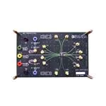
Figure 1. Evaluation Board
Rev. 0
Information furnished by Analog Devices is believed to be accurate and reliable. However, no
responsibility is assumed by Analog Devices for its use, nor for any infringements of patents or other
rights of third parties that may result from its use. Specifications subject to change without notice. No
license is granted by implication or otherwise under any patent or patent rights of Analog Devices.
Trademarks and registered trademarks are the property of their respective owners.
One Technology Way, P.O. Box 9106, Norwood, MA 02062-9106, U.S.A.
Tel: 781.329.4700
www.analog.com
Fax: 781.461.3113
©2006 Analog Devices, Inc. All rights reserved.
�EVAL-ADCMP565
TABLE OF CONTENTS
Features ...................................................................................... 1
Outputs ..................................................................................3
Applications............................................................................... 1
Evaluation Board Layout .........................................................4
Product Description................................................................. 1
Typical Connection Diagram..............................................4
ADCMP565 Device Description............................................ 1
Schematic...............................................................................5
Revision History ....................................................................... 2
Layers .....................................................................................7
Evaluation Board Hardware .................................................... 3
Ordering Information ............................................................13
Power Supplies ...................................................................... 3
Ordering Guide...................................................................13
Inputs ..................................................................................... 3
ESD Caution........................................................................13
Latches ................................................................................... 3
REVISION HISTORY
1/06—Revision 0: Initial Version
Rev. 0 | Page 2 of 16
�EVAL-ADCMP565
EVALUATION BOARD HARDWARE
POWER SUPPLIES
INPUTS
Power is supplied via color-coded banana jack plugs and all are
decoupled on the board.
There are four separate input pins on the ADCMP565.
Likewise, there are four input SMA connectors distinctively
labeled on this evaluation board. AC signals should be directly
applied to one of these four input SMAs. If a dc threshold is
desired, a small network is supplied that allows one dc source to
be connected to any input pin and then changed as desired. The
actual threshold is supplied via the blue banana jacks on both
COMP A and COMP B. A connection is then from the banana
jack (DC THRESHOLD IN) to an SMA connector (DC
THRESHOLD OUT). From this point, the threshold can be
jumpered using an SMA cable to any input pin desired.
•
Red is +5 V.
•
Yellow is –5.2 V.
•
Green is –4 V. The –4 V is not required by the part. Rather,
this voltage is used to provide proper on-board ECL
terminations for the part.
•
Two black jacks are for ground.
•
Two blue jacks are labeled DC THRESHOLD IN. For
proper use of the blue jacks, see the Inputs section.
Table 1. Connector Functions
Name
J1
J2
J3
J4
J5
J6
J7
J8
J9
J10
J11
J12
J13
J14
TP1 (Black)
TP2 (Red)
TP3 (Yellow)
TP4 (Green)
TP5 (Blue)
TP6 (Blue)
TP9 (Black)
Function
Threshold_A Out
Threshold_B Out
QAbar
QA
QB
QBbar
LEAbar
LEA
LEBbar
LEB
IB+
IA+
IA−
IB−
GND
VCC
VEE
−4V
Threshold_A In
Threshold_B In
GND
Note that every input trace continues by the pin and through a
50 Ω resistor to ground. This provides the option of using high
speed AD signals for every input being used. If using a dc
threshold on one of the input pins is desired, it is advisable to
remove the 50 Ω resistor for that pin depending on how much
current the supply can deliver. R1, R2, R3, and R4 correspond
respectively to inputs IB, IA, IB, and IA.
LATCHES
Each half of the dual comparator has a latch enable and an
inverted latch enable pin. These pins should be directly driven
by connecting a source to each SMA connector. It is important
to remember that the latches cannot be left unconnected.
Proper levels must be provided for the ADCMP565 to function
correctly. For correct logic levels in both compare and latch
modes, please refer to the pin description in the ADCMP565
data sheet.
OUTPUTS
A resistor network on each output trace provides a very
accurate ECL 50 Ω path to the output SMA connectors. By
using any SMA-compatible cable, the outputs can be monitored
on the 50 Ω equipment of the user’s choice.
Rev. 0 | Page 3 of 16
�EVAL-ADCMP565
EVALUATION BOARD LAYOUT
The EVAL-ADCMP565 is designed to ensure that a high fidelity 50 Ω environment is maintained from input to output. Trace widths are
carefully matched with the PCB material to produce a 50 Ω transmission line. Trace lengths are matched exactly for all inputs and latches.
All outputs are also matched in length to each other. For specific part/pin information on the ADCMP565, please refer to the data sheet.
TYPICAL CONNECTION DIAGRAM
50Ω SIGNAL SOURCES
COAX
JUMPER
DC POWER SUPPLIES
50Ω SCOPE INPUTS
THRESHOLD
VOLTAGE
ADCMP565
COAX
JUMPER
50Ω SIGNAL SOURCES
Figure 2.
Rev. 0 | Page 4 of 16
05823-002
THRESHOLD
VOLTAGE
�EVAL-ADCMP565
SCHEMATIC
J3
J4
J6
J5
2OB
AGND
AGND
AGND
20B
AGND
20A
R6
2OA
49. 9
R7
R5
49. 9
49. 9
0
J9
R19
R11
R8
49. 9
AGND
- 4V
R13
R15
100
100
R14
R18
4
18
GND
5
17
L EB
AGND
J10
7
15
L EB
VEE
8
14
V CC
R1 6
L EA
49. 9
16
ADCMP565
0
20
. 1UF
OB
R9
0
R10
49. 9
AGND
C15
GND
6
AGND
C14
L EA
AGND
J7
1
OA
3
. 1UF
. 1UF
100
OB
OA
19
100
C13
2
C12
AGND
49. 9
- 4V
. 1UF
J8
R2 4
R17
49. 9
AGND
C19
13
12
11
9
C21
AGND
10
AGND
AGND
AGND
IB
IA
. 1UF
C20
IA
0
AGND
R1 2
. 1UF
C18
IB
VEE
100PF
VCC
100PF
AGND
AGND
AGND
R4
R3
R2
49. 9
R1
49. 9
AGND
J13
AGND
49. 9
49. 9
J12
J11
J14
AGND
AGND
Figure 3.EVAL-ADCMP565 Schematic, Page 1 of 2
Rev. 0 | Page 5 of 16
AGND
05823-003
AGND
�EVAL-ADCMP565
TP2
RED
1
VCC
TP1
BLK
+
C26
10µF
C10
0.1µF
C7
0.1µF
C8
0.1µF
C9
0.1µF
1
TP3
AGND
YEL
1
VEE
+
TP4
C27
10µF
C11
0.1µF
C16
0.1µF
C17
0.1µF
C22
0.1µF
AGND
GRN
1
–4V
+
TP5
C28
10µF
C25
0.1µF
AGND
J1
THRESHOLD_A
+
C29
10µF
C4
0.1µF
C5
0.1µF
C6
0.1µF
AGND
BLU
THRESHOLD_B
1
TP9
C24
0.1µF
BLU
1
TP6
C23
0.1µF
BLK
+
C30
10µF
C1
0.1µF
C2
0.1µF
J2
C3
0.1µF
AGND
Figure 4. EVAL-ADCMP565 Schematic, Page 2 of 2
Rev. 0 | Page 6 of 16
05823-004
1
�EVAL-ADCMP565
LAYERS
05823-006
05823-007
ADCMP565
The ADCMP565 evaluation board consists of eight layers (including both signal and power planes). The following pages represent
these layers.
Figure 6. Primary Solder Mask
Figure 5. Primary Silkscreen
Rev. 0 | Page 7 of 16
�Figure 7. Layer 1 (Signal)
05823-009
05823-008
EVAL-ADCMP565
Figure 8. Layer 2 (GND 1)
Rev. 0 | Page 8 of 16
�05823-010
05823-011
EVAL-ADCMP565
Figure 10. Layer 4 (VEE)
Figure 9. Layer 3 (−4 V)
Rev. 0 | Page 9 of 16
�05823-012
05823-013
EVAL-ADCMP565
Figure 12. Layer 6 (VCC)
Figure 11. Layer 5 (GND2)
Rev. 0 | Page 10 of 16
�Figure 13. Layer 7 (GND 3)
05823-015
05823-014
EVAL-ADCMP565
Figure 14. Layer 8 (Signal)
Rev. 0 | Page 11 of 16
�Figure 15. Secondary Solder Mask
05823-017
05823-016
EVAL-ADCMP565
Figure 16. Secondary Silkscreen
Rev. 0 | Page 12 of 16
�EVAL-ADCMP565
ORDERING INFORMATION
ORDERING GUIDE
Model
EVAL-ADCMP565BP
Description
Evaluation Board
ESD CAUTION
ESD (electrostatic discharge) sensitive device. Electrostatic charges as high as 4000 V readily accumulate on
the human body and test equipment and can discharge without detection. Although this product features
proprietary ESD protection circuitry, permanent damage may occur on devices subjected to high energy
electrostatic discharges. Therefore, proper ESD precautions are recommended to avoid performance
degradation or loss of functionality.
Rev. 0 | Page 13 of 16
�EVAL-ADCMP565
NOTES
Rev. 0 | Page 14 of 16
�EVAL-ADCMP565
NOTES
Rev. 0 | Page 15 of 16
�EVAL-ADCMP565
NOTES
©2006 Analog Devices, Inc. All rights reserved. Trademarks and
registered trademarks are the property of their respective owners.
EB05823-0-1/06(0)
Rev. 0 | Page 16 of 16
�
很抱歉,暂时无法提供与“EVAL-ADCMP565BPZ”相匹配的价格&库存,您可以联系我们找货
免费人工找货- 国内价格
- 1+1653.72840
- 200+659.84760
- 500+637.80480
- 1000+626.90760