Evaluation Board for ADCMP572/
ADCMP573/ADCMP580/ADCMP581/ADCMP582
EVAL-ADCMP572/573/580/581/582
GENERAL DESCRIPTION
EVALUATION BOARD DESCRIPTION
This document provides an overview and suggested lab test setups
of the evaluation board for Analog Devices’ new ADCMP572/
ADCMP573/ADCMP580/ADCMP581/ADCMP582 comparator
products. Because these comparators represent state of the art,
general-purpose comparator technology, it is important that their
performance characteristics be evaluated using the highest bandwidth components available. The evaluation board provides a
relatively high quality environment in which to make such
measurements. All five device types are fully released to
production.
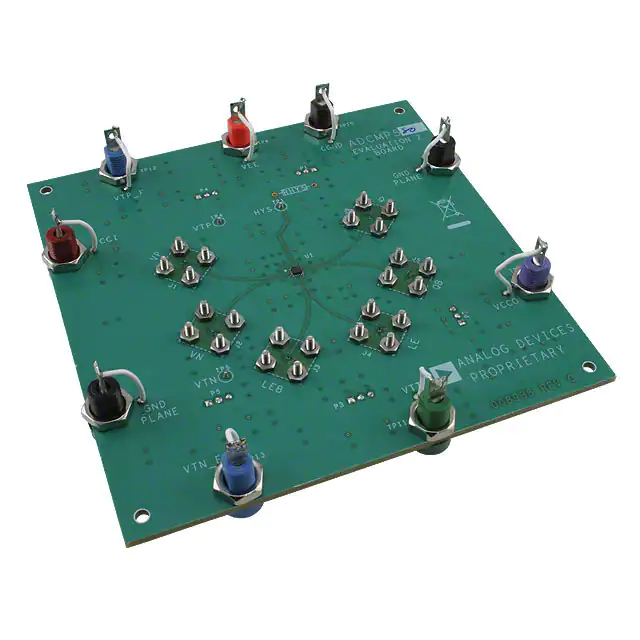
Figure 1 is a photograph of the top of the evaluation board. It is
fabricated using a high quality dielectric material between the
ground plane and signal layers in order to maintain high signal
integrity. All input and output signals are brought on to the
board with 2.9 mm RF connectors, and transmission line paths
are kept as close to 50 Ω as possible.
PACKAGE LIST
•
Evaluation board with component installed
•
Schematic
This document should be used in conjunction with the
ADCMP57x/ADCMP58x data sheets that contain full technical
details on the device specifications and operation. The same
PCB is used to evaluate the ADCMP572, ADCMP573,
ADCMP580, ADCMP581, and ADCMP580.
05821-001
EVALUATION BOARD
Figure 1. ADCMP572/ADCMP573/ADCMP580/ADCMP581/ADCMP5822 Evaluation Board
Rev. 0
Information furnished by Analog Devices is believed to be accurate and reliable. However, no
responsibility is assumed by Analog Devices for its use, nor for any infringements of patents or other
rights of third parties that may result from its use. Specifications subject to change without notice. No
license is granted by implication or otherwise under any patent or patent rights of Analog Devices.
Trademarks and registered trademarks are the property of their respective owners.
One Technology Way, P.O. Box 9106, Norwood, MA 02062-9106, U.S.A.
Tel: 781.329.4700
www.analog.com
Fax: 781.461.3113
©2006 Analog Devices, Inc. All rights reserved.
�EVAL-ADCMP572/573/580/581/582
TABLE OF CONTENTS
General Description ......................................................................... 1
Setup Input Signals........................................................................8
Evaluation Board Description......................................................... 1
Connect Output Signals ...............................................................8
Package List ....................................................................................... 1
Jumper Setup......................................................................................9
Evaluation Board .............................................................................. 1
Test Setup......................................................................................... 10
Revision History ............................................................................... 2
Additional Support..................................................................... 10
Using the Evaluation Board............................................................. 3
Schematics ....................................................................................... 11
Measurements ............................................................................... 3
Ordering Information.................................................................... 20
Setting Up the Evaluation Board .................................................... 4
Ordering Guide .......................................................................... 20
Connect Power.............................................................................. 4
ESD Caution................................................................................ 20
Connect Inputs ............................................................................. 8
REVISION HISTORY
2/06—Revision 0: Initial Version
Rev. 0 | Page 2 of 20
�EVAL-ADCMP572/573/580/581/582
USING THE EVALUATION BOARD
MEASUREMENTS
Table 1. Basic Equipment
The same PCB is used to evaluate both ADCMP57x and
ADCMP58x families. The Setting Up the Evaluation Board
section describes the measurements that can be performed with
this evaluation board.
Description
Power Supply with
Three Outputs
Pulse Generator
Signal Analyzer
Source Meter
Matched High Speed
Cables with 2.9 mm
Connectors
1
2
Example Equipment 1
Agilent E3631A
Quantity
2
HP8133A, Agilent 81134A
CSA 8000 with 80E04
sampling head 2
Keithley 2400 SourceMeter,
Keithley 238 high current
source-measure unit
Insulated Wire Inc. kps1501-180-kps
Florida RF LABS LAB-FLEX
160 2Y194
1
1
1
4
Equipment used to generate example measurements within this document.
20 GHz sampling head used for all time measurements.
Rev. 0 | Page 3 of 20
�EVAL-ADCMP572/573/580/581/582
SETTING UP THE EVALUATION BOARD
CONNECT POWER
Several power supply levels must be provided to the board for
VCCI, VCCO, VEE, VTT, CGND (the comparator’s GND pin), and
GND via the banana jacks. Make a direct connection from the
DUT output pins to the oscilloscope because any transmission
line discontinuity degrades performance.
The flexible power supply scheme of the ADCMP572/ADCMP573
comparators can be confusing with VTT at system ground. The
GND pin on the comparator is no longer at GND dc potential,
except for the ADCMP580, and, therefore, is named CGND on the
board.
Because of this, VTT is always at GND and therefore, VCCO = VTT
(GND) + 2.0 V for the ECL/PECL ADCMP573/ADCMP581/
ADCMP582, and VCCO = VTT = GND for the CML type
ADCMP572 and GND = CGND = VTT only for the CML
ADCMP580, as detailed in Table 2 through Table 4.
Table 2. ADCMP580/ADCMP581 Power Supply Connections
Pin No.
5, 16
9, 12
13
14
8
15
ADCMP580 (CML) 1
5.0 V
0.0 V
−5.0 V
−5.0 V
0V
0.0 V
0V
Mnemonic
VCCI (Red)
GND (Purple) (also CGND for these devices)
VEE (Orange)
HYS (Orange)
VTT (Green)
CGND (Brown) 3
GND Plane (Black) 4
ADCMP581(NECL) 2
7.0 V
2.0 V
−3.0 V
−3.0 V
0V
2.0 V
0V
1
VCCI = 5.0 V, VCCO = 0 V, VEE = −5.0 V.
VCCI = 5.0 V, VCCO = 0 V, VEE = −5.0 V.
3
CGND is the comparator ground (Pin 15) renamed.
4
GND is always system ground.
2
VCCI
VCCI
VP
2
GND
+
VTP
VP
9, 12
11
ADCMP580
VN
VTN
HYS
14
13
15
8
+
9, 12
11
ADCMP581
10
VTN
VTT
LE INPUT
HYS
LE INPUT
Q OUTPUT
–
4
14
13
15
7 6
8
VTT
LE INPUT
LE INPUT
VEE GND
05821-023
VEE GND
NOTES
1. FOR ADCMP580 CGND = GND.
3
Q OUTPUT
RSECL
Q OUTPUT
VN
7 6
GND
Q OUTPUT
–
4
2
CML
10
3
5, 16
1
NOTES
1. GND HERE BECOMES BOARD CGND.
Figure 3. ADCMP581 Power Supply Connections
Figure 2. ADCMP580 Power Supply Connections
Rev. 0 | Page 4 of 20
05821-024
VTP
5, 16
1
�EVAL-ADCMP572/573/580/581/582
Table 3. ADCMP582 Power Supply Connections
Pin No.
5, 16
9, 12
13
14
8
15
Mnemonic
VCCI (Red)
VCCO (Purple)
VEE (Orange)
HYS
VTT (Green)
CGND (Brown) 3
GND Plane (Black) 4
ADCMP582(PECL) 1
2.0 V
2.0 V
−8.0 V
−8.0 V
0V
−3.0 V
0V
ADCMP582(PECL) 2
3.7 V
2.0 V
−6.3 V
−6.3 V
0V
−1.3 V
0V
ADCMP582(PECL)
4.5 V
2.0 V
−5.5 V
−5.5 V
0V
−0.5 V
0V
1
VCCI = 5.0 V, VCCO = 5.0 V, VEE = −5.0 V.
VCCI = 5.0 V, VCCO = 3.3 V, VEE = −5.0 V.
3
CGND is the comparator ground (Pin 15) renamed.
4
GND is always system ground.
2
VCCI
VTP
VP
5, 16
1
2
VCCO
+
9, 12
11
ADCMP582
RSPECL
10
VN
VTN
HYS
3
Q OUTPUT
Q OUTPUT
–
4
14
13
15
7 6
8
VTT
LE INPUT
LE INPUT
NOTES
1. GND HERE BECOMES BOARD CGND.
Figure 4. ADCMP582 Power Supply Connections
Rev. 0 | Page 5 of 20
05821-025
VEE GND
�EVAL-ADCMP572/573/580/581/582
Table 4. ADCMP572 Power Supply and Input Translation
Pin
VCCI
VCCO
CGND
VTP_F/VTN_F
VTT
VP/VN
LE/LE
AGND
(This is not a pin in the part.)
Case 1 1
0.0 V
0.0 V
−3.3 V
0V
0.0 V
−3.5V < VN/VP