EVAL-ADG5298EB1Z User Guide
UG-1038
One Technology Way • P.O. Box 9106 • Norwood, MA 02062-9106, U.S.A. • Tel: 781.329.4700 • Fax: 781.461.3113 • www.analog.com
Evaluating the ADG5298, High Temperature, High Voltage, Latch-Up Proof,
8-Channel Multiplexer
FEATURES
GENERAL DESCRIPTION
o
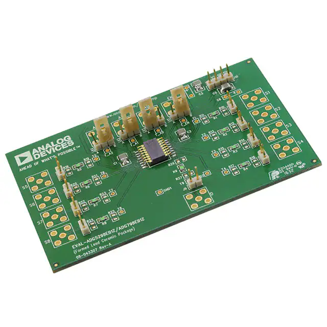
The EVAL-ADG5298EB1Z is the evaluation board for the
ADG5298 high temperature 8:1 multiplexer. The board assembly
is constructed with high temperature compliant materials and is
suitable for short duration evaluation up to 210°C.
Up to 210 C high temperature operation
Supply voltages
Dual supply: ±5 V to ±22 V
Single supply: 8 V to 44 V
Parallel interface compatible with 3 V logic
Figure 1 shows the EVAL-ADG5298EB1Z in a typical evaluation
setup. The ADG5298 is soldered to the center of the EVALADG5298EB1Z evaluation board, and headers are provided to
connect to each of the source and drain pins. A 4-pin header
powers the device and provides a user defined digital logic
supply voltage.
EVALUATION KIT CONTENTS
EVAL-ADG5298EB1Z evaluation board
ONLINE RESOURCES
Documents Needed
ADG5298 data sheet
EVAL-ADG5298EB1Z user guide
EQUIPMENT NEEDED
DC voltage source
±22 V for dual supply
44 V for single supply
Digital logic supply: 3 V to 5 V
Analog signal source
Method to measure voltage, such as a digital multimeter (DMM)
Full specifications on the ADG5298 are available in the
ADG5298 data sheet, which should be consulted in conjunction
with this user guide when using the EVAL-ADG5298EB1Z
evaluation board.
TYPICAL EVALUATION SETUP
POWER SUPPLY
14945-001
SIGNAL GENERATOR
Figure 1. EVAL-ADG5298EB1Z, Power Supply, and Signal Generator
PLEASE SEE THE LAST PAGE FOR AN IMPORTANT
WARNING AND LEGAL TERMS AND CONDITIONS.
Rev. 0 | Page 1 of 10
�UG-1038
EVAL-ADG5298EB1Z User Guide
TABLE OF CONTENTS
Features .............................................................................................. 1
Input Signals...................................................................................4
Evaluation Kit Contents ................................................................... 1
Board Construction ......................................................................4
Online Resources .............................................................................. 1
Jumper Settings ..................................................................................5
Equipment Needed ........................................................................... 1
Switches and 0 Ω Resistors...........................................................5
General Description ......................................................................... 1
SMB Connectors............................................................................5
Typical Evaluation Setup ................................................................. 1
Decoupling Capacitors .................................................................5
Revision History ............................................................................... 2
Evaluation Board Schematics and Artwork ...................................6
Getting Started .................................................................................. 3
Ordering Information .................................................................... 10
Evaluation Board Setup Procedure ............................................ 3
Bill of Materials ........................................................................... 10
Evaluation Board Hardware ............................................................ 4
Power Supply ................................................................................. 4
REVISION HISTORY
9/2016—Revision 0: Initial Version
Rev. 0 | Page 2 of 10
�EVAL-ADG5298EB1Z User Guide
UG-1038
GETTING STARTED
EVALUATION BOARD SETUP PROCEDURE
Take the following steps to set up a functionality test:
The EVAL-ADG5298EB1Z evaluation board operates
independently and does not require any additional evaluation
boards or software to operate.
1.
Connect a power supply to J10. Connect VSS and GND
together if a single supply is required.
LK1 through LK4 control the digital signals for the
ADG5298. See Table 1 for the logic control truth table.
2.
Supply the EVAL-ADG5298EB1Z evaluation board with a dual
power source of up to ±22 V or a single supply of up to +44 V
by connecting VSS and GND together.
J10
VDD
VDD
ADG5298
J1:S1
S1
LK1
J9:D
D
J8:S8
J10
LK2
VL
LK3
S8
EN
A0
A1
A2
1-OF-8
DECODER
GND
VSS
LK4
J10
14945-002
GND
VSS
Figure 2. EVAL-ADG5298EB1Z Block Diagram of the Main Components
Rev. 0 | Page 3 of 10
�UG-1038
EVAL-ADG5298EB1Z User Guide
EVALUATION BOARD HARDWARE
The operation of the ADG5298 is evaluated using the EVALADG5298EB1Z. Figure 1 shows a typical evaluation setup
where only a power supply and signal generator are required.
Figure 2 shows the block diagram of the main components of
the EVAL-ADG5298EB1Z evaluation board.
Using this evaluation board, the ADG5298 passes signals from
either the source or the drain connectors.
POWER SUPPLY
Connector J10 provides access to the supply pins of the ADG5298.
VDD, GND, and VSS on the J10 link to the appropriate pins on
the ADG5298. For dual-supply voltages, the EVAL-ADG5298EB1Z
evaluation board can be powered from ±5 V to ±22 V. For singlesupply voltages, the GND and VSS terminals must be connected
together, and the EVAL-ADG5298EB1Z evaluation board must
be powered with 8 V to 44 V. In addition, use the J10 header to
supply the voltage, VL, used to control the digital logic.
INPUT SIGNALS
Headers connect to both the source and drain pins of the
ADG5298. Additional Subminiature Version B (SMB) connector
pads are available if extra connections are required.
Each trace on the source and drain side includes two sets of
0805 pads, which can place a load on the signal path to ground.
A 0 Ω resistor is placed in the signal path and can be replaced
with a user defined value. The resistor combined with the 0805
pads can create a simple resistor capacitor (RC) filter.
The ADG5298 uses a parallel interface to control the operation
of the switches. The switch operation can be manually controlled
using the LK1 to LK4 switches, or an external controller can be
interfaced directly to the control pins by using the SMB connector
pads, if required (EN, A0, A1, and A2). See Table 1 for the logic
control truth table.
BOARD CONSTRUCTION
The board assembly uses high temperature rated components,
including passives, connectors, printed circuit board (PCB)
materials, and solder. By using a polyimide PCB laminate, it can
handle a high glass transition temperature (TG), allowing it to
maintain integrity at high temperatures where standard laminate
deteriorates. The EVAL-ADG5298EB1Z evaluation board uses a
Sn90Sb10 lead free solder due to its high melting point (245°C to
250°C). The EVAL-ADG5298EB1Z evaluation board also uses a
nickel gold surface finish (plating) to avoid intermetallic formation
between the tin in the solder and the copper PCB traces at high
temperatures. In addition, the EVAL-ADG5298EB1Z evaluation
board uses resistors, capacitors, and connectors rated for extended
temperatures by their respective manufacturers. For further
information on the EVAL-ADG5298EB1Z evaluation board
construction, see the bill of materials in Table 3.
Rev. 0 | Page 4 of 10
�EVAL-ADG5298EB1Z User Guide
UG-1038
JUMPER SETTINGS
SWITCHES AND 0 Ω RESISTORS
DECOUPLING CAPACITORS
Links control the ADG5298 manually. Table 1 and Table 2 show
the truth table and the summary of the links.
The EVAL-ADG5298EB1Z evaluation board comes with 0.1 µF
decoupling capacitors populated on both the VDD and VSS
power supplies, which provides sufficient decoupling for the
ADG5298. However, if extra decoupling is needed due to for
example, a noisy power supply, C4 and C6 can add additional
decoupling capacitors.
Use LK2 to LK4 to control the switches of the ADG5298.
Position L is tied to GND and sets the logic low, and Position H
is tied to VL and sets the logic high.
Use LK1 to enable or disable the device. Position L is tied to
GND and disables the device, and Position H is tied to VL and
enables the device.
SMB CONNECTORS
The parallel interface of the ADG5298 is controlled manually
using the link headers (LK1 to LK4), or it can be accessed using the
SMB front prints (EN, A0, A1, and A2). Note that these
footprints are unpopulated.
Table 1. ADG5298 Truth Table
LK4 (A2)
Don’t care
Low
Low
Low
Low
High
High
High
High
LK3 (A1)
Don’t care
Low
Low
High
High
Low
Low
High
High
LK2 (A0)
Don’t care
Low
High
Low
High
Low
High
Low
High
LK1 (EN)
Low
High
High
High
High
High
High
High
High
Table 2. Switch and 0 Ω Resistor Descriptions
Label
LK1
LK2
LK3
LK4
Position
Low
High
Low
High
Low
High
Low
High
Description
Logic 0 on the EN pin
Logic 1 on the EN pin
Logic 0 on the A0 pin
Logic 1 on the A0 pin
Logic 0 on the A1 pin
Logic 1 on the A1 pin
Logic 0 on the A2 pin
Logic 1 on the A2 pin
Rev. 0 | Page 5 of 10
Connected Sx
All switches off
S1
S2
S3
S4
S5
S6
S7
S8
�UG-1038
EVAL-ADG5298EB1Z User Guide
14945-003
EVALUATION BOARD SCHEMATICS AND ARTWORK
Figure 3. EVAL-ADG5298EB1Z Evaluation Board Schematic (Part 1)
Rev. 0 | Page 6 of 10
�UG-1038
14945-004
EVAL-ADG5298EB1Z User Guide
Figure 4. EVAL-ADG5298EB1Z Evaluation Board Schematic (Part 2)
Rev. 0 | Page 7 of 10
�EVAL-ADG5298EB1Z User Guide
14945-005
UG-1038
14945-006
Figure 5. EVAL-ADG5298EB1Z Silkscreen
Figure 6. EVAL-ADG5298EB1Z Top Layer
Rev. 0 | Page 8 of 10
�UG-1038
14945-007
EVAL-ADG5298EB1Z User Guide
Figure 7. EVAL-ADG5298EB1Z Bottom Layer
Rev. 0 | Page 9 of 10
�UG-1038
EVAL-ADG5298EB1Z User Guide
ORDERING INFORMATION
BILL OF MATERIALS
Table 3.
Reference Designator
A0 to A2, EN, S1 to S8, D
C1 to C3, C5
C4, C6
T1 to T9, T_A0 to T_A2,
T_EN, GND1, GND2
J1 to J9
J10
R1 to R9
R10 to R27
LK1 to LK4
U1
Not Applicable
Description
50 Ω, straight, SMB jacks
0.1 µF ceramic capacitors, 100 V, NP0, 1210
Through hole, electrolytic capacitors
Test points
Manufacturer Part Number
Not applicable
C1210H104J1GACTU
Not applicable
Not applicable
Stock Code
Do not insert
Digi-Key 399-5748-2-ND
Do not insert
Do not insert
Vertical, high temperature series, through
hole, headers, 2-pin, 2.54 mm
Vertical, high temperature series, through
hole, headers, 4-pin, 2.54 mm
0 Ω, 0805, 0.125 W, maximum operating
temperature = 300oC
SMD, 0805, resistors
Vertical, high temperature series, through
hole, headers, 3-pin, 2.54 mm and shorting link
High temperature, high voltage, latch-up proof,
8-channel multiplexer
Solder, Sn90Sb10 alloy
YMC02SAAN
Digi-Key S9665-02-ND
YMC04SAAN
Digi-Key S9665-04-ND
SPJ3003-0RN1
SPJ3003-0RN1
Not applicable
YMC03SAAN and
WDC02SXNN
ADG5298HFRZ
Do not insert
Digi-Key S9665-03-ND and
Digi-Key S9663-ND
ADG5298HFRZ
Indium Corporation Indalloy
259 solder paste, 8.9 HF
Not applicable
ESD Caution
ESD (electrostatic discharge) sensitive device. Charged devices and circuit boards can discharge without detection. Although this product features patented or proprietary protection
circuitry, damage may occur on devices subjected to high energy ESD. Therefore, proper ESD precautions should be taken to avoid performance degradation or loss of functionality.
Legal Terms and Conditions
By using the evaluation board discussed herein (together with any tools, components documentation or support materials, the “Evaluation Board”), you are agreeing to be bound by the terms and conditions
set forth below (“Agreement”) unless you have purchased the Evaluation Board, in which case the Analog Devices Standard Terms and Conditions of Sale shall govern. Do not use the Evaluation Board until you
have read and agreed to the Agreement. Your use of the Evaluation Board shall signify your acceptance of the Agreement. This Agreement is made by and between you (“Customer”) and Analog Devices, Inc.
(“ADI”), with its principal place of business at One Technology Way, Norwood, MA 02062, USA. Subject to the terms and conditions of the Agreement, ADI hereby grants to Customer a free, limited, personal,
temporary, non-exclusive, non-sublicensable, non-transferable license to use the Evaluation Board FOR EVALUATION PURPOSES ONLY. Customer understands and agrees that the Evaluation Board is provided
for the sole and exclusive purpose referenced above, and agrees not to use the Evaluation Board for any other purpose. Furthermore, the license granted is expressly made subject to the following additional
limitations: Customer shall not (i) rent, lease, display, sell, transfer, assign, sublicense, or distribute the Evaluation Board; and (ii) permit any Third Party to access the Evaluation Board. As used herein, the term
“Third Party” includes any entity other than ADI, Customer, their employees, affiliates and in-house consultants. The Evaluation Board is NOT sold to Customer; all rights not expressly granted herein, including
ownership of the Evaluation Board, are reserved by ADI. CONFIDENTIALITY. This Agreement and the Evaluation Board shall all be considered the confidential and proprietary information of ADI. Customer may
not disclose or transfer any portion of the Evaluation Board to any other party for any reason. Upon discontinuation of use of the Evaluation Board or termination of this Agreement, Customer agrees to
promptly return the Evaluation Board to ADI. ADDITIONAL RESTRICTIONS. Customer may not disassemble, decompile or reverse engineer chips on the Evaluation Board. Customer shall inform ADI of any
occurred damages or any modifications or alterations it makes to the Evaluation Board, including but not limited to soldering or any other activity that affects the material content of the Evaluation Board.
Modifications to the Evaluation Board must comply with applicable law, including but not limited to the RoHS Directive. TERMINATION. ADI may terminate this Agreement at any time upon giving written notice
to Customer. Customer agrees to return to ADI the Evaluation Board at that time. LIMITATION OF LIABILITY. THE EVALUATION BOARD PROVIDED HEREUNDER IS PROVIDED “AS IS” AND ADI MAKES NO
WARRANTIES OR REPRESENTATIONS OF ANY KIND WITH RESPECT TO IT. ADI SPECIFICALLY DISCLAIMS ANY REPRESENTATIONS, ENDORSEMENTS, GUARANTEES, OR WARRANTIES, EXPRESS OR IMPLIED, RELATED
TO THE EVALUATION BOARD INCLUDING, BUT NOT LIMITED TO, THE IMPLIED WARRANTY OF MERCHANTABILITY, TITLE, FITNESS FOR A PARTICULAR PURPOSE OR NONINFRINGEMENT OF INTELLECTUAL
PROPERTY RIGHTS. IN NO EVENT WILL ADI AND ITS LICENSORS BE LIABLE FOR ANY INCIDENTAL, SPECIAL, INDIRECT, OR CONSEQUENTIAL DAMAGES RESULTING FROM CUSTOMER’S POSSESSION OR USE OF
THE EVALUATION BOARD, INCLUDING BUT NOT LIMITED TO LOST PROFITS, DELAY COSTS, LABOR COSTS OR LOSS OF GOODWILL. ADI’S TOTAL LIABILITY FROM ANY AND ALL CAUSES SHALL BE LIMITED TO THE
AMOUNT OF ONE HUNDRED US DOLLARS ($100.00). EXPORT. Customer agrees that it will not directly or indirectly export the Evaluation Board to another country, and that it will comply with all applicable
United States federal laws and regulations relating to exports. GOVERNING LAW. This Agreement shall be governed by and construed in accordance with the substantive laws of the Commonwealth of
Massachusetts (excluding conflict of law rules). Any legal action regarding this Agreement will be heard in the state or federal courts having jurisdiction in Suffolk County, Massachusetts, and Customer hereby
submits to the personal jurisdiction and venue of such courts. The United Nations Convention on Contracts for the International Sale of Goods shall not apply to this Agreement and is expressly disclaimed.
©2016 Analog Devices, Inc. All rights reserved. Trademarks and
registered trademarks are the property of their respective owners.
UG14945-0-9/16(0)
Rev. 0 | Page 10 of 10
�


 工商网监
湘ICP备2023018690号
工商网监
湘ICP备2023018690号
