EVAL-ADHV4702-1CPZ User Guide
UG-1444
One Technology Way • P.O. Box 9106 • Norwood, MA 02062-9106, U.S.A. • Tel: 781.329.4700 • Fax: 781.461.3113 • www.analog.com
Evaluating the ADHV4702-1 24 V to 220 V Precision Operational Amplifier
FEATURES
EVAL-ADHV4702-1CPZ PHOTOGRAPHS
Full featured evaluation board for the ADHV4702-1
Single-supply or dual-supply operation
On-board power management circuit generates high voltage
Edge mounted SMA and SMB connector provisions
Easy connection to test equipment and other circuits
Robust thermal management
EVALUATION KIT CONTENTS
EVAL-ADHV4702-1CPZ evaluation board
DOCUMENTS NEEDED
17224-001
ADHV4702-1 data sheet
LT8304-1 data sheet
This user guide describes the EVAL-ADHV4702-1CPZ evaluation board, which helps users evaluate the ADHV4702-1 offered in
a 7 mm × 7 mm, 12-lead lead frame chip scale package (LFCSP)
with an exposed pad at the bottom. The evaluation board provides
a platform for quick and easy evaluation of the ADHV4702-1.
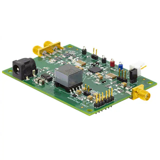
Figure 1 shows the top side of the evaluation board. Figure 2
shows the bottom side of the board with the large exposed
copper area for attaching a heat sink to provide additional
thermal management.
The evaluation board is a 6-layer board designed to minimize
leakage currents with its guard ring feature. It accepts Subminiature Version A (SMA) and Subminiature Version B (SMB) edge
mounted connectors on the inputs for easy connection to test
equipment or other circuitry.
The ADHV4702-1 data sheet covers the specifications and details
of the device operation and application circuit configurations
and guidance. Full specifications of the ADHV4702-1 can be
found in the ADHV4702-1 data sheet, available from Analog
Devices, Inc., and must be consulted in conjunction with this
user guide, especially when powering up the evaluation board
for the first time.
For safety, the EVAL-ADHV4702-1CPZ evaluation board is
covered top and bottom with acrylic plastic guards to reduce
the risk of inadvertent contact with high voltage. Do not operate
the board without these guards in place. If the guards must be
removed to adjust jumpers or change component values, disconnect the board from the power supply before removing guards,
and replace the guards before powering up again. For full
precautions when using this high voltage evaluation board, see
the High Voltage Evaluation Board section.
PLEASE SEE THE LAST PAGE FOR AN IMPORTANT
WARNING AND LEGAL TERMS AND CONDITIONS.
Rev. 0 | Page 1 of 10
Figure 1. Evaluation Board, Top
17224-002
GENERAL DESCRIPTION
Figure 2. Evaluation Board, Bottom
�UG-1444
EVAL-ADHV4702-1CPZ User Guide
TABLE OF CONTENTS
Features .............................................................................................. 1
Shutdown Feature (SDN Connector) .........................................4
Evaluation Kit Contents ................................................................... 1
Input Clamping Diodes ................................................................4
Documents Needed .......................................................................... 1
Input Guard Ring ..........................................................................4
General Description ......................................................................... 1
Thermal Monitor/Flag (TMP) and Thermal Management .....4
EVAL-ADHV4702-1CPZ Photographs ......................................... 1
Resistor Adjustable Quiescent Current (RADJ) ........................4
Revision History ............................................................................... 2
Evaluation Board Schematics...........................................................5
Evaluation Board Hardware ............................................................ 3
Ordering Information .......................................................................7
Board Stackup ............................................................................... 3
Bill of Materials ..............................................................................7
Initial Power-Up ........................................................................... 3
High Voltage Evaluation Board .......................................................9
Power Supplies and Decoupling ................................................. 3
Warnings, Restrictions, and Disclaimers ...................................9
Input and Output .......................................................................... 3
Digital Ground (DGND) ............................................................. 3
REVISION HISTORY
11/2018—Revision 0: Initial Version
Rev. 0 | Page 2 of 10
�EVAL-ADHV4702-1CPZ User Guide
UG-1444
EVALUATION BOARD HARDWARE
BOARD STACKUP
The EVAL-ADHV4702-1CPZ evaluation board is a 6-layer
board. The signal routings are on Layer 1 (top) and Layer 4. The
bottom layer is an exposed copper ground plane used for heat
dissipation and heat sink attachment. Internal Layer 2 through
Layer 5 are the VCC, VMID, signal, and VEE planes,
respectively.
The EVAL-ADHV4702-1CPZ evaluation board is divided into
two sections as shown in Figure 3. The upper section is the test
circuit for the ADHV4702-1, and the lower section is the
optional on-board power management circuit comprising an
LT8304-1 monolithic micropower isolated flyback converter. The
connection of these two sections can be made via the P1, P4,
and P5 connectors. Refer to the Initial Power-Up section for
more information.
test circuit via the P1, P4, and P5 connectors. For ±110 V dual
supplies, jump VCC_TRANSFORMER to VCC, VEE_
TRANSFORMER to VEE, and GND_TRANSFORMER to
AGND. The LT8304-1 on-board power management circuit can
also provide a single supply of 220 V. The schematic for the
on-board power management circuit is shown in Figure 5. For
more information, refer to the LT8304-1 data sheet for different
voltage output options.
POWER SUPPLIES AND DECOUPLING
The EVAL-ADHV4702-1CPZ evaluation board can be powered
using a single supply or dual supplies. The total supply voltage
(VCC − VEE) must be between 24 V and 220 V. When using a
single supply or asymmetrical dual supplies, apply the appropriate
reference voltage to the VMID pin of P2 using a low impedance
source, such as a dc power supply. The recommended VMID
reference voltage is (VCC + VEE)/2.
ADHV4702-1 TEST CIRCUIT
The EVAL-ADHV4702-1CPZ board provides sufficient power
supply decoupling for fast slewing signals with 1.2 µF (C1, C2),
250 V ceramic chip capacitors where the supply voltage enters
the board. Two 0.1 µF, 250 V ceramic chip capacitors (C3, C5)
are placed in close proximity to VCC at Pin 7. Two capacitors
(C4, C6) are placed in close proximity to VEE at Pin 4.
LT8304-1 POWER MANAGEMENT CIRCUIT
17224-003
INPUT AND OUTPUT
Figure 3. Evaluation Board Test and Power Management Circuits
INITIAL POWER-UP
The EVAL-ADHV4702-1CPZ evaluation board is shipped for
use with dual symmetrical power supplies. Before applying
power to the board, apply the jumper from the VMID node to
the AGND node (see Figure 4) via P2, using the 2-pin header, to
provide a dc operating point for the amplifier.
The EVAL-ADHV4702-1CPZ evaluation board can be powered
up using the external power supply or the on-board LT8304-1
power management circuit. To power up the board using an
external power supply, apply the power at the PWR header or
via the GND, VCC, and VEE test points. The quiescent supply
current is approximately 3 mA. In addition to the quiescent
current, there is an additional ~2.2 mA from the VCC supply to
bias the D1 Zener diode clamp at the SDN connector.
The LT8304-1 on-board power management circuit can be used
to provide dual supplies of approximately ±110 V from a
convenient 15 V dc input. Apply 15 V dc from an external
power supply at the VIN_15V test point or by using a 15 V dc
wall transformer type plugin at P6. Connect the outputs from
the on-board power management circuit to the ADHV4702-1
Figure 4 and Figure 5 show the evaluation board schematics for
the factory default settings. The evaluation board uses edge
mount SMA connectors on the inputs and outputs for easy
interfacing to signal sources and test equipment. In addition,
the board accepts SMB connectors on the inputs for efficient
connection to other circuitry such as the EVAL-AD5754REBZ
DAC evaluation board.
The EVAL-ADHV4702-1CPZ evaluation board is equipped
with 49.9 Ω termination resistors at R1 and R2. The power
rating of the termination resistors is 1 W, which are capable of
handling the power when using the factory default settings. The
termination resistance can be removed or replaced with a
different value based on the output impedance of the selected
input signal source.
The EVAL-ADHV4702-1CPZ evaluation board accommodates
a default 10 kΩ, 1210 resistor load (R25) to VMID, or a 1210
capacitor load referenced to AGND. The EVAL-ADHV4702-1CPZ
evaluation board is in a default noninverting configuration with
a gain of ~21 V/V and a feedback resistance of 39.2 kΩ. In this
configuration, the amplifier delivers about 10 mA peak to the
load at the maximum output swing.
DIGITAL GROUND (DGND)
The DGND pin sets a common signal ground for communication
to a microprocessor or other low voltage logic circuit. The
DGND pin voltage is also the reference for all the low voltage
pins of the amplifier such as RADJ, TMP, and SD. DGND is
connected to the 0 V AGND on the evaluation board.
Rev. 0 | Page 3 of 10
�UG-1444
EVAL-ADHV4702-1CPZ User Guide
SHUTDOWN FEATURE (SDN CONNECTOR)
The SD pin of the ADHV4702-1 can be jumped to logic high,
logic low, or can be left floating via the SDN connector on the
EVAL-ADHV4702-1CPZ evaluation board.
The SD pin is left floating at the SDN connector as shipped
from the factory, enabling the amplifier. Pulling the SD pin low
to DGND places the amplifier in a power saving shutdown
mode. When turning the amplifier back on from the shutdown
state, float the SD pin or pull it high.
INPUT CLAMPING DIODES
To protect the amplifier from high dynamic power dissipation,
the EVAL-ADHV4702-1CPZ evaluation board is configured by
default with input clamping diodes (D6 and D7) that clamp the
input differential voltage of the ADHV4702-1 at a two-diode
forward bias voltage. This input clamping network limits the
drive to the slew boosting circuit, which affects dynamic performance such as bandwidth and slew rate. The recommended
part number for the input clamping diodes is SBAV199LT1G.
Removing the input clamping diodes allows the slew boosting
circuit to be fully biased, which maximizes slew rate and
improves settling time significantly. The fully biased slew
boosting circuit requires additional supply current and results
in higher power dissipation during slewing. For reliable
operation, always operate the amplifier within the safe
operating area curve and provide additional heat sinking as
required for the application. Refer to the ADHV4702-1 data
sheet for more information.
INPUT GUARD RING
The EVAL-ADHV4702-1CPZ evaluation board employs an
electrostatic guard ring on the top layer to reduce printed
circuit board (PCB) surface leakage currents. The guard ring
encircles the noninverting input and must be biased at the same
voltage as the input. The guard ring can be biased using a
voltage source at P3 or connected to the noninverting input by
installing a 0 Ω resistor at R10. Remove the input clamping
diodes (D6 and D7) to ensure the complete enclosure of the
high impedance input node.
THERMAL MONITOR/FLAG (TMP) AND THERMAL
MANAGEMENT
The TMP pin can be used to monitor relative changes in die
temperature. The typical TMP pin voltage at room temperature
is approximately 1.9 V and changes at approximately −4.5 mV/°C.
More precise temperature readings can be achieved through a
single-point (offset) ambient temperature calibration. This
calibration can be accomplished by measuring the TMP pin to
establish the precise voltage corresponding to ambient temperature. To avoid calibration error due to self heating, power up the
device in shutdown mode (hold SD low at supply turn on) and
maintain it in shutdown mode until the TMP pin voltage is
measured.
The TMP pin can be connected to the SD pin by installing a 0 Ω
resistor at R8 to enable the overtemperature and short-circuit
protection features. Install a resistor at RTEMP to set the thermal
shutdown threshold temperature. Refer to the ADHV4702-1
data sheet for more information about the temperature monitor
and short-circuit protection.
The ADHV4702-1 evaluation board is designed with an
exposed copper top layer for robust thermal management.
Solder the exposed pad (EPAD) of the package to the copper
layer to ensure optimal thermal dissipation. The top exposed
copper area is connected to the exposed copper ground plane
on the bottom by an array of five thermal vias. In addition, a
heat sink can be attached to the bottom exposed ground plane
to increase the power dissipation capability of the ADHV4702-1.
RESISTOR ADJUSTABLE QUIESCENT CURRENT
(RADJ)
The EVAL-ADHV4702-1CPZ evaluation board is configured by
default with a 0 Ω RADJ resistor that fully biases the amplifier
and sets the supply current to 3 mA. Increasing the value of
RADJ reduces the quiescent current, lowering the bandwidth
and slew rate of the amplifier while also reducing quiescent
power dissipation. Refer to the ADHV4702-1 data sheet for
more information about RADJ.
Rev. 0 | Page 4 of 10
�VEE
22-12-2034
AGND
Figure 4. EVAL-ADHV4702-1CPZ Evaluation Board Device Under Test Circuit Schematic
C2
1.2UF
250V
C1
1.2UF
250V
SDN
49.9K
R11
SD
HI
SDN
LO
AGND
C6
0.1UF
250V
AGND
C5
0.1UF
250V
AGND
AGND
C7
0.1UF
250V
VMID
VCC
AGND
D1
BZX84C5V6LT1/T3G
1
2
3
C4
0.1UF
250V
C3
0.1UF
250V
TSW-103-08-G-S
AGND
VEE
VCC
BYPASS CAPS AND ESD PROTECTION
AGND
GND1
AGND
INN1
AGND
INP1
VCC
VCC
RED
1
142134
1
AGND
2 3 4 5
INN
142134
142-0701-801
AGND
2 3 4 5
INP
142-0701-801
VEE
VEE
BLU
AGND
R2
49.9
R2512
INN_TP
5015
TBD1210
DNI
RINN
VMID
DNI
R4
TBD1206
0
R1206
0
R1206
0
R1210
49.9
R2512
AGND
R1
R5
INP_TP1
5015
GRD1
R3
AGND
1
2
RINP
INP_TP
5015
69157-102HLF
AGND
1
2
VMID
RG
2K
INN_TP1
5015
GRD
R9
DNI
R0603
D6
GND
BLKBLK
R10
DNI
R0603
AGND
2
VCC
SDN
IN–
IN+
VEE
12
GRD1
R8
TBD0603
DNI
R23
TBD0603
DNI
DNI
C9
TBD1210
0
1
2
3
0
VCC
BAV199LT1G
P3
69157-102HLF
7
VCC
P2
BAV199LT1G
VMID
D7
8
RFB
2PF
250V
CFB
39.2K
PAD
POWER CONNECTORS
R12
VEE
4
DGND
10
Rev. 0 | Page 5 of 10
49.9K
3
0
RADJ
AGND
AGND
R26
0
ADHV4702-1BCPZ
OUT
A1
R24
TBD0603
DNI
6
AGND
100K
RTEMP
TMP
5015
SD
PAD
9
RADJ
1
RESERVED
5
TMP
RESERVED
11
COMP
PWR
AGND
R27
0
OUT
5015
CLOAD
TBD1210
DNI
0
R1210
R6
RCOMP
TBD1206
DNI
CCOMP
TBD1210
DNI
AGND
R25
10K
0
R1210
R7
VMID
AGND
142-0701-801
VOUT
EVAL-ADHV4702-1CPZ User Guide
UG-1444
EVALUATION BOARD SCHEMATICS
17224-004
�R28
0
Rev. 0 | Page 6 of 10
C11
10PF
AGND
C8
22UF
C
A
R29
2.4K
C10
22UF
AGND
Figure 5. EVAL-ADHV4702-1CPZ Evaluation Board On-Board Power Management Schematic
AGND
R13
10K
7
1
DS1
SML-D12P8WT86
0
R30
C20
47UF
INTVCC
2
5
SW
6
RFB
U1
AGND
N
P
VIN_15V
R15
12.7K
R14
AGND
AGND
R16
100
D3
CMMR1U-06 TR
510K
C13
270PF
SMAJ70A
D2
4
3
2
1
P6
KLDX-SMT2-0202-ATR
AGND
8
C12
TC
1UF
PAD GND
PAD
4 LT8304HS8E-1#PBF
RREF
3
VIN
EN/UVLO
VIN_15V
WHT 1
VCC
P1
NS1
NS2
T1
10
9
7
6
TSW-103-08-G-S
1
2
3
NC NC NC NC
1 3 5 8
NP
CEP1311F
4
2
AGND
VCC_TRANSFORMER
C14
0.22UF
CMMR1U-06 TR
D4
C15
0.22UF
CMMR1U-06 TR
D5
1
2
3
P4
200
200
R22
R18
200
200
R17
R21
C17
0.22UF
C16
0.22UF
TSW-103-08-G-S
VEE
VEE_TRANSFORMER
AGND
C19
0.22UF
C18
0.22UF
AGND
1
2
P5
R20
200K
R19
200K
VEE_TRANSFORMER
GND_TRANSFORMER
VCC_TRANSFORMER
69157-102HLF
GND_TRANSFORMER
UG-1444
EVAL-ADHV4702-1CPZ User Guide
17224-005
�EVAL-ADHV4702-1CPZ User Guide
UG-1444
ORDERING INFORMATION
BILL OF MATERIALS
Table 1. Bill of Materials
Item
1
Qty.
1
Reference Designator
Not applicable
2
3
1
2
A1
C1, C2
4
5
6
2
1
1
C8, C10
C11
C12
7
8
1
6
C13
C14, C15, C16, C17, C18, C19
9
10
11
12
13
14
1
5
1
1
1
3
C20
C3, C4, C5, C6, C7
CFB
D1
D2
D3, D4, D5
Description
EVAL-ADHV4702-1CPZ evaluation
board
ADHV4702-1
Ceramic capacitor, X7R, C2225H61,
250 V
Ceramic capacitor, X5R, C1210, 25 V
Ceramic capacitor, C0805, 100 V
Ceramic capacitor, X7R, C0805H53,
50 V
Ceramic capacitor, NP0, C0805, 50 V
Ceramic capacitor, X7R, C1210,
220 V
Capacitor, tantalum, C3528, 16 V
Ceramic capacitor, X7R, 1210, 250 V
Ceramic capacitor, C0603, 250 V
Diode, Zener, SOT-23, 5.6 V
Diode, DO-214AC
Diode, SOD123F, 600 V
15
16
17
2
1
2
D6, D7
DS1
GND, GND1
Diode, SOT-23, 70 V
LED
Connector, test point
18
19
2
3
INN, INP
INN1, INP1, VOUT
Connector, SMB
Connector, SMA end launch
20
6
Connector, test points
21
3
INN_TP, INN_TP1, INP_TP,
INP_TP1, OUT, TMP
P1, P4, SDN
22
3
P2, P3, P5
23
24
25
26
27
28
29
30
31
32
33
34
35
36
37
38
39
40
1
1
2
2
1
1
1
1
4
2
1
5
1
1
1
3
1
1
P6
PWR
R1, R2
R11, R12
R13
R14
R15
R16
R17, R18, R21, R22
R19, R20
R25
R26, R27, R28, R30, RADJ
R29
R3
R5
R6, R7, RINP
RFB
RG
Connector, PCB, Berg, header,
straight, male, 3-position
Connector, PCB, Berg, header,
straight, male, 2-position
Connector, PCB dc power jack
Connector, PCB, header, right angle
Resistor, 2512, 1%, 500 V
Resistor, 1206, 0.1%
Resistor, 0805, 1%
Resistor, 0805, 1%
Resistor, 0805, 1%
Resistor, 1206, 1%
Resistor, 1206, 1%
Resistor, 1206, 1%
Resistor, 1210, 0.1%
Resistor, 0603, 1%, 50 V
Resistor, 0603, 1%, 50 V
Resistor, 1206
Resistor, 1206
Resistor, 1210, 200 V
Resistor, 1206, 1%
Resistor, 1206, 1%
Rev. 0 | Page 7 of 10
Manufacturer
Analog Devices
Part Number
08_044831c
Analog Devices
Kemet
ADHV4702-1BCPZ
C2225C125KARACTU
Murata
AVX
Murata
GRM32ER61E226KE15L
08051A100JAT2A
GRM21BR71H105KA12B
Yageo
AVX Corporation
CC0805JRNP09BN271
12102C224KAT2A
AVX Corporation
TDK
Murata
On Semiconductor
Littelfuse
Central
Semiconductor
On Semiconductor
Rohm
Components
Corporation
Amphenol
Cinch Connectivity
Solutions
Keystone Electronics
TCNL476M016R0250
C3225X7R2E104K
GQM1875C2E2R0BB12
BZX84C5V6LT1/T3G
SMAJ70A
CMMR1U-06 TR LEAD
FREE
BAV199LT1G
SML-D12P8WT86
TP-104-01-00
Samtec
TSW-103-08-G-S
Amphenol FCI
69157-102HLF
Kycon
MOLEX
VISHAY
Susumu Co, LTD
PANASONIC
ROHM
PANASONIC
BOURNS
PANASONIC
PANASONIC
PANASONIC
Multicomp (SPC)
Panasonic
Vishay
Panasonic
Vishay
Panasonic
Panasonic
KLDX-SMT2-0202-ATR
22-12-2034
CRCW251249R9FKEG
RG3216P-4992-B-T5
ERJ-6ENF1002V
MCR10EZHF5103
ERJ-6ENF1272V
CRS1206-FX-1000ELF
ERJ-8ENF2000V
ERJ-8ENF2003V
ERA-14EB103U
MC0603WG00000T5E-TC
ERJ-3EKF2401V
CRCW12060000Z0EAHP
ERJ-8GEY0R00V
CRCW12100000Z0EAHP
ERJ-8ENF3922V
ERJ-8ENF2001V
142134
142-0701-801
5015
�UG-1444
EVAL-ADHV4702-1CPZ User Guide
Item
41
42
43
Qty.
1
1
1
Reference Designator
T1
U1
VCC
Description
Transformer
LT8304-1
Connector, PCB, test point, red
44
1
VEE
Connector, PCB, test point, blue
45
1
VIN_15V
Connector, PCB, test point, white
Rev. 0 | Page 8 of 10
Manufacturer
Sumida
Analog Devices
Components
Corporation
Components
Corporation
Components
Corporation
Part Number
13324-T196
LT8304HS8E-1#PBF
TP-104-01-02
TP104-01-06
TP-104-01-09
�EVAL-ADHV4702-1CPZ User Guide
UG-1444
HIGH VOLTAGE EVALUATION BOARD
Warning: this high voltage evaluation board contains exposed metal carrying lethal voltages when under power. Take all necessary steps
to protect users during operation.
WARNINGS, RESTRICTIONS, AND DISCLAIMERS
For evaluation only, in laboratory or development environments, by professionals trained to handle high voltage devices. This
evaluation board is not a finished electrical equipment and not intended for consumer use. It is intended solely for use for preliminary
feasibility evaluation in laboratory or development environments by technically qualified electronics experts who are familiar with the
dangers and application risks associated with handling high voltage electrical components, systems, and subsystems. It is not to be used as
all or part of a finished end product.
Your Responsibility and Risk. You acknowledge, represent, and agree that
1.
2.
3.
4.
You have knowledge of all federal, state and local regulatory requirements that relate to your products and that relate to your use
(and/or that of your employees, affiliates, contractors, or designees) of the evaluation board for evaluation, testing, and other
purposes.
You have full and exclusive responsibility to assure the safety and compliance of your products with all such laws and other applicable
regulatory requirements, and also to assure the safety of any activities to be conducted by you and/or your employees, affiliates,
contractors, or designees, using the evaluation board. Further, you are responsible to assure that any interfaces (electronic and/or
mechanical) between the evaluation board and any human body are designed with suitable isolation and means to safely limit
accessible leakage currents to minimize the risk of electrical shock hazard.
You must employ reasonable safeguards to ensure that your use of the evaluation board does not result in any property damage,
injury, or death, even if the evaluation board fails to perform as described or expected.
You must properly dispose of or recycle the electronic components of the evaluation board to avoid injury to any other person.
Key Instructions. It is important to operate this evaluation board within Analog Devices recommended specifications and environmental
considerations per the user guidelines. Exceeding the specified evaluation board ratings (including but not limited to input and
output voltage, current, power, temperature, and environmental ranges) may cause property damage, personal injury, or death. If
there are questions concerning these ratings, contact an Analog Devices representative prior to connecting interface electronics or loads.
Any loads applied outside of the specified output range may result in unintended and/or inaccurate operation and/or possible permanent
damage to the evaluation board and/or interface electronics. Consult the evaluation board user guide prior to connecting any load to the
evaluation board output. If there is uncertainty as to the load specification, contact an Analog Devices representative. During normal
operation, some circuit components may generate significant heat, which may cause fire, melting, or burns. When placing measurement
probes near these devices during normal operation, be aware that these devices may be hot. As with all electronic evaluation tools, only
qualified personnel knowledgeable in electronic measurement and diagnostics are to use the evaluation board.
Agreement to Defend, Indemnify and Hold Harmless. You agree to defend, indemnify, and hold Analog Devices, its directors, officers,
employees, and their representatives harmless from and against any and all claims, damages, losses, expenses, costs, and liabilities
(collectively, "Claims") arising out of or in connection with any use of the evaluation board that is not in accordance with the terms of the
agreement. This obligation applies whether Claims arise under law of tort or contract or any other legal theory, and even if the evaluation
board fails to perform as described or expected.
Rev. 0 | Page 9 of 10
�UG-1444
EVAL-ADHV4702-1CPZ User Guide
NOTES
ESD Caution
ESD (electrostatic discharge) sensitive device. Charged devices and circuit boards can discharge without detection. Although this product features patented or proprietary protection
circuitry, damage may occur on devices subjected to high energy ESD. Therefore, proper ESD precautions should be taken to avoid performance degradation or loss of functionality.
Legal Terms and Conditions
By using the evaluation board discussed herein (together with any tools, components documentation or support materials, the “Evaluation Board”), you are agreeing to be bound by the terms and conditions
set forth below (“Agreement”) unless you have purchased the Evaluation Board, in which case the Analog Devices Standard Terms and Conditions of Sale shall govern. Do not use the Evaluation Board until you
have read and agreed to the Agreement. Your use of the Evaluation Board shall signify your acceptance of the Agreement. This Agreement is made by and between you (“Customer”) and Analog Devices, Inc.
(“ADI”), with its principal place of business at One Technology Way, Norwood, MA 02062, USA. Subject to the terms and conditions of the Agreement, ADI hereby grants to Customer a free, limited, personal,
temporary, non-exclusive, non-sublicensable, non-transferable license to use the Evaluation Board FOR EVALUATION PURPOSES ONLY. Customer understands and agrees that the Evaluation Board is provided
for the sole and exclusive purpose referenced above, and agrees not to use the Evaluation Board for any other purpose. Furthermore, the license granted is expressly made subject to the following additional
limitations: Customer shall not (i) rent, lease, display, sell, transfer, assign, sublicense, or distribute the Evaluation Board; and (ii) permit any Third Party to access the Evaluation Board. As used herein, the term
“Third Party” includes any entity other than ADI, Customer, their employees, affiliates and in-house consultants. The Evaluation Board is NOT sold to Customer; all rights not expressly granted herein, including
ownership of the Evaluation Board, are reserved by ADI. CONFIDENTIALITY. This Agreement and the Evaluation Board shall all be considered the confidential and proprietary information of ADI. Customer may
not disclose or transfer any portion of the Evaluation Board to any other party for any reason. Upon discontinuation of use of the Evaluation Board or termination of this Agreement, Customer agrees to
promptly return the Evaluation Board to ADI. ADDITIONAL RESTRICTIONS. Customer may not disassemble, decompile or reverse engineer chips on the Evaluation Board. Customer shall inform ADI of any
occurred damages or any modifications or alterations it makes to the Evaluation Board, including but not limited to soldering or any other activity that affects the material content of the Evaluation Board.
Modifications to the Evaluation Board must comply with applicable law, including but not limited to the RoHS Directive. TERMINATION. ADI may terminate this Agreement at any time upon giving written notice
to Customer. Customer agrees to return to ADI the Evaluation Board at that time. LIMITATION OF LIABILITY. THE EVALUATION BOARD PROVIDED HEREUNDER IS PROVIDED “AS IS” AND ADI MAKES NO
WARRANTIES OR REPRESENTATIONS OF ANY KIND WITH RESPECT TO IT. ADI SPECIFICALLY DISCLAIMS ANY REPRESENTATIONS, ENDORSEMENTS, GUARANTEES, OR WARRANTIES, EXPRESS OR IMPLIED, RELATED
TO THE EVALUATION BOARD INCLUDING, BUT NOT LIMITED TO, THE IMPLIED WARRANTY OF MERCHANTABILITY, TITLE, FITNESS FOR A PARTICULAR PURPOSE OR NONINFRINGEMENT OF INTELLECTUAL
PROPERTY RIGHTS. IN NO EVENT WILL ADI AND ITS LICENSORS BE LIABLE FOR ANY INCIDENTAL, SPECIAL, INDIRECT, OR CONSEQUENTIAL DAMAGES RESULTING FROM CUSTOMER’S POSSESSION OR USE OF
THE EVALUATION BOARD, INCLUDING BUT NOT LIMITED TO LOST PROFITS, DELAY COSTS, LABOR COSTS OR LOSS OF GOODWILL. ADI’S TOTAL LIABILITY FROM ANY AND ALL CAUSES SHALL BE LIMITED TO THE
AMOUNT OF ONE HUNDRED US DOLLARS ($100.00). EXPORT. Customer agrees that it will not directly or indirectly export the Evaluation Board to another country, and that it will comply with all applicable
United States federal laws and regulations relating to exports. GOVERNING LAW. This Agreement shall be governed by and construed in accordance with the substantive laws of the Commonwealth of
Massachusetts (excluding conflict of law rules). Any legal action regarding this Agreement will be heard in the state or federal courts having jurisdiction in Suffolk County, Massachusetts, and Customer hereby
submits to the personal jurisdiction and venue of such courts. The United Nations Convention on Contracts for the International Sale of Goods shall not apply to this Agreement and is expressly disclaimed.
©2018 Analog Devices, Inc. All rights reserved. Trademarks and
registered trademarks are the property of their respective owners.
UG17224-0-11/18(0)
Rev. 0 | Page 10 of 10
�