EVAL-ADM2582EEMIZ/EVAL-ADM2587EEMIZ User Guide
UG-916
One Technology Way • P.O. Box 9106 • Norwood, MA 02062-9106, U.S.A. • Tel: 781.329.4700 • Fax: 781.461.3113 • www.analog.com
2-Layer EN55022 Class A Radiated Emissions Compliant Evaluation Board for the
ADM2582E/ADM2587E 2.5 kV rms Signal and Power Isolated RS-485 Transceivers
with ±15 kV ESD Protection
FEATURES
GENERAL DESCRIPTION
2.5 kV rms power and signal isolated RS-485/RS-422 transceiver
PCB layout optimized for EN55022 radiated emissions
according to the AN-1349 Application Note
ADM2587E passes EN55022 Class A (certification available)
ADM2582E passes EN55022 Class A (certification available)
2-layer printed circuit board (PCB) layout that minimizes PCB
material cost
Convenient connections for power and signal through screw
terminal blocks
Configurable as half-duplex or full-duplex
5 V or 3.3 V operation
Easily configurable through jumper connections
Test points for measuring all signals
The ADM2582E/ADM2587E evaluation board can easily
evaluate the ADM2582E and ADM2587E power and signal
isolated RS-485/RS-422 transceivers. Screw terminal blocks
provide convenient connections for the power and signal
connections. The evaluation board is easily configured through
jumper connections. The board can be used in half-duplex or fullduplex configurations and has a 120 Ω termination resistor
fitted on the receiver input. The evaluation board can be used
with either the ADM2582E 16 Mbps device or the ADM2587E
500 kbps device. The driver and receiver are enabled and disabled
by jumper connections. Test points are included on the power
and signal lines on both sides of the isolation barrier.
EVALUATION KIT CONTENTS
The ADM2582E/ADM2587E evaluation board is designed to
reduce emissions generated by the high frequency switching
elements used by the isoPower® technology to transfer power
through the ADM2582E/ADM2587E integrated transformer.
The layout of the evaluation board is generated using the
guidelines provided in the AN-1349 Application Note, PCB
Implementation Guidelines to Minimize Radiated Emissions on
the ADM2582E/ADM2587E RS-485/RS-422 Transceivers. The
ADM2587E and ADM2582E evaluation boards are tested and
certified to pass EN55022 Class A.
EN55022 RADIATED EMISSIONS
EVAL-ADM2582EEMIZ or EVAL-ADM2587EEMIZ
DOCUMENTS NEEDED
AN-1349 Application Note
ADM2582E/ADM2587E data sheet
14003-001
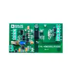
EVALUATION BOARD PHOTOGRAPH
Figure 1.
PLEASE SEE THE LAST PAGE FOR AN IMPORTANT
WARNING AND LEGAL TERMS AND CONDITIONS.
Rev. 0 | Page 1 of 12
�UG-916
EVAL-ADM2582EEMIZ/EVAL-ADM2587EEMIZ User Guide
TABLE OF CONTENTS
Features .............................................................................................. 1
Termination and Pull-Up/Pull-Down Resistors .......................4
Evaluation Kit Contents ................................................................... 1
Decoupling and Reservoir Capacitors ........................................4
Documents Needed .......................................................................... 1
Board Internal Layer Thickness ..................................................4
General Description ......................................................................... 1
PCB Layout Reccomendations ....................................................4
EN55022 Radiated Emissions ......................................................... 1
EN55022 Radiated Emissions Test Results ................................5
Evaluation Board Photograph......................................................... 1
Evaluation Board Schematics and Artwork ...................................8
Revision History ............................................................................... 2
Ordering Information .................................................................... 10
Evaluation Board Hardware ............................................................ 3
Bill of Materials ........................................................................... 10
Test Setup ....................................................................................... 3
Related Links ............................................................................... 11
Jumper Settings ............................................................................. 3
REVISION HISTORY
5/2016—Revision 0: Initial Version
Rev. 0 | Page 2 of 12
�EVAL-ADM2582EEMIZ/EVAL-ADM2587EEMIZ User Guide
UG-916
EVALUATION BOARD HARDWARE
TEST SETUP
JUMPER SETTINGS
The ADM2582E/ADM2587E evaluation board is shown
in Figure 2 with the default jumper settings on the LK1 through
LK9 jumper blocks. In the default jumper connections, both the
ADM2582E/ADM2587E driver and receiver are enabled. Figure 2
also shows the power connection on the J2 terminal block, input
signal connection on the DI jack, and probes attached to the RXD,
DI, Y, and Z test points for a loopback test (LK5 and LK7 are
closed to connect A to Y pins and B to Z pins, respectively).
The inputs to the ADM2582E/ADM2587E can be configured
using the jumpers on the evaluation board (see Table 1). Do not
place multiple jumper blocks on the LK1, LK3, and LK6 jumper
blocks because the input sources may be shorted together. For
each link, a single jumper block can move from one position to
another, as specified in Table 1.
SIGNAL
GENERATOR
OSCILLOSCOPE
LK6
J3
RXD
LK1
RE
DE
DI
C
B
A
C
B
A
LK3
GND1
GND2
RxD
RE
DE
DI
A
B
Z
Y
A
LK5
B
Z
LK7
Y
DI
LK9
J2
GND
C
B
A
VDD
SHIELD
GND
J4
EVAL-ADM2582EEMIZ/87EEMIZ
14003-002
3.3V OR 5V
POWER
SUPPLY
Figure 2. Basic Operation of the EN55022 Class A Compliant Evaluation Board for the ADM2582E/ADM2587E Isolated RS-485/RS-422 Transceivers
Table 1. Jumper Configuration
Link
LK1
LK6
LK3
LK9
Connection
A
B
C
A
B
C
Closed
LK5
A
B
C
Closed
LK7
Open
Closed
Open
Description
Connects the driver enable input (DE) of the ADM2582E/ADM2587E to VCC pin. This setting enables the driver.
Connects the driver enable input (DE) of the ADM2582E/ADM2587E to the DE J3 terminal block connector.
Connects the driver enable input (DE) of the ADM2582E/ADM2587E to GND1pin. This setting disables the driver.
Connects the receiver enable input (RE) of the ADM2582E/ADM2587E to VCC pin. This setting disables the receiver.
Connects the receiver enable input (RE) of the ADM2582E/ADM2587E to the RE J3 terminal block connector.
Connects the receiver enable input (RE) of the ADM2582E/ADM2587E to GND1 pin. This setting enables the receiver.
Connects the receiver enable input (RE) of the ADM2582E/ADM2587E to the driver enable input (DE). This setting
ensures that when the driver is enabled, the receiver is disabled, or when the driver is disabled, the receiver is enabled.
Connects the TxD pin of the ADM2582E/ADM2587E to the DI connector.
Connects the TxD pin of the ADM2582E/ADM2587E to the DI J3 terminal block connector.
Connects the TxD pin of the ADM2582E/ADM2587E to the on-board oscillator circuit.
Connects the ADM2582E/ADM2587E Receiver Input B to Driver Output Z. When LK5 and LK7 are both
connected, the evaluation board is configured for half-duplex operation.
When LK5 and LK7 are both open, the evaluation board is configured for full-duplex operation.
Connects the ADM2582E/ADM2587E Receiver Input A to Driver Output Y. When LK5 and LK7 are both connected,
the evaluation board is configured for half-duplex operation.
When LK5 and LK7 are both open, the evaluation board is configured for full-duplex operation.
Rev. 0 | Page 3 of 12
�UG-916
EVAL-ADM2582EEMIZ/EVAL-ADM2587EEMIZ User Guide
TERMINATION AND PULL-UP/PULL-DOWN
RESISTORS
PCB LAYOUT RECCOMENDATIONS
The evaluation board includes the RT and RT1 footprints for
fitting termination resistors between the A and B receiver inputs
and the Y and Z driver outputs. By default, the board is not
fitted with a 120 Ω resistor, RT, between A and B. This resistor
must be removed if the board is connected to a bus that is
already terminated at both ends. For more information about
proper termination, see the AN-960 Application Note, RS485/RS-422 Circuit Implementation Guide.
Although the ADM2582E/ADM2587E have a built-in receiver
fail-safe for the bus idle condition, there are footprints on the
evaluation board for fitting the R9 and R10 pull-up resistors to
the VISOOUT supply of the ADM2582E/ADM2587E on A and Y,
as well as the R7 and R8 pull-down resistors to GND2 on B and Z.
These resistors can be fitted if the user is connecting to other
devices that require external biasing resistors on the bus. The
exact value required for a 200 mV minimum differential voltage
in the bus idle condition depends on the supply voltage (for
example, 960 Ω for 3.3 V and 1440 Ω for 5 V).
For more information about the bus idle fail-safe, see the AN-960
Application Note, RS-485/RS-422 Circuit Implementation Guide.
DECOUPLING AND RESERVOIR CAPACITORS
The evaluation board uses the following decoupling and
reservoir capacitors:
•
•
•
•
On the logic side of the board, the C3 and C4 capacitors
must be 10 nF and 100 nF ceramic capacitors, respectively,
and the C2 capacitor must be a 10 µF tantalum capacitor.
On the logic side of the board, the C7 capacitor must be a
100 nF ceramic capacitor, and the C9 capacitor must be a
10 µF tantalum capacitor.
On the logic side of the board additional capacitors are
added for the power regulation circuits. C12, C13, and C16
must be a 10 µF tantalum capacitors, while C14 and C15
must be 100 nF ceramic capacitors.
On the bus side of the board, the C5 and C6 capacitors
must be 10 nF and 100 nF, respectively, and the C1 and
C98 capacitors must be 100 nF and 10 µF, respectively.
BOARD INTERNAL LAYER THICKNESS
The ADM2582E/ADM2587E evaluation board consists of two
layers. The spacing between the top and bottom layer is 1.6 mm.
The EVAL-ADM2582EEMIZ and EVAL-ADM2587EEMIZ PCB
has a layer spacing of 0.4 mm between Layer 1 and Layer 2,
meeting requirements for isolation standards IEC 61010, third
edition, and IEC 60950 in the AN-1109 Application Note,
Recommendations for Control of Radiated Emissions with iCoupler
Devices.
The ADM2582E/ADM2587E evaluation board is designed to
reduce emissions generated by the high frequency switching
elements used by the isoPower technology to transfer power
through the ADM2582E/ADM2587E integrated transformer.
The layout of the evaluation board is generated using the
guidelines provided in the AN-1349 Application Note.
The AN-1349 Application Note provides examples of 4-layer PCBs.
The EVAL-ADM2582EEMIZ and EVAL-ADM2587EEMIZ PCB
layout is a 2-layer PCB. To pass EN55022 Class A on a 2-layer
PCB, the following layout guidelines are recommended:
•
Ensure that there is good decoupling on the PCB (see the
Decoupling and Reservoir Capacitors section).
• Place a ferrite bead between the PCB trace connections and
the following IC pins: VISOOUT (Pin 12) and GND2 (Pin 11
and Pin 14).
• Do not connect the VISOOUT pin to a power plane;
connect between VISOOUT and VISOIN using a PCB trace.
Ensure VISOIN (Pin 19) is connected through the L3 ferrite
to VISOOUT (Pin 12) as shown in Figure 3.
• Place a high voltage discrete capacitor connected between
GND1 (Pin 10) and GND2 (Pin 11).The EVALADM2582EEMIZ requires a high voltage discrete capacitor
in order to pass EN 55022 Class A with adequate margin to
allow for test variation. However, the EVAL-ADM2587EEMIZ
can pass EN 55022 Class A without a high voltage discrete
capacitor. Adding a high voltage discrete capacitor to the
EVAL-ADM2587EEMIZ allows a larger pass margin from
the EN55022 Class A limits.
The following additional notes apply to the PCB layout; refer to
the schematic and artwork in Figure 10 to Figure 13.
• Ensure GND2 (Pin 14) is connected to GND2 (Pin 11) on
the inside (device side) of the C1 100 nF capacitor.
• Ensure the C1 capacitor is connected between VISOOUT
(Pin 12) and GND2 (Pin 11) on the device side of the L2
and L3 ferrites.
• Ensure GND2 (Pin 16) is connected to GND2 (Pin 11) on
the outside (bus side) of the L2 ferrite as shown in Figure 3.
• Ensure that there is a keep out area for the GND2 plane in
the PCB layout around the L2 and L3 ferrites. The keep
out area means there must not be a GND2 fill on any layer
below the L2 and L3 ferrites.
• Ensure there is a minimum of 4 mm separation gap
between the GND2 plane fill and the GND2 fill for the C19
high voltage discrete capacitor pad.
Rev. 0 | Page 4 of 12
�EVAL-ADM2582EEMIZ/EVAL-ADM2587EEMIZ User Guide
UG-916
Table 2. EN55022 Test Results Summary
Device
ADM2587E
ADM2582E
ADM2582E
Locate the power delivery circuit in close proximity to the
ADM2587E/ADM2582E device, so the VCC trace is as
short as possible. The EVAL-ADM2582EEMIZ and
EVAL-ADM2587EEMIZ PCB has a power delivery circuit
located at the bottom of the PCB with a short trace from
the ADP667ARZ regulator output to VCC (Pin 8). This
layout example minimizes the loop area in which high
frequency current can flow. An increase in the loop area
results in an increase in the emissions levels.
EN55022 RADIATED EMISSIONS TEST RESULTS
The ADM2587E evaluation board is tested and certified to pass
EN55022 Class A with >6 dbμV margin. The ADM2582E
evaluation board is tested and certified to pass EN55022 Class A.
EN55022 Certification documents for the EVAL-ADM2582EEMIZ
and EVAL-ADM2587EEMIZ evaluation boards are available to
customers upon request from Analog Devices, Inc.
Table 3 provides a summary of the capability of the EVALADM2582EEMIZ and EVAL-ADM2587EEMIZ evaluation boards.
All EN55022 radiated emissions tests are performed with the PCB
schematic and layout as described in Figure 10 to Figure 13. The
C19 capacitor (See Figure 10) high voltage discrete capacitor is
removed for some tests. Table 2 describes the effect of removing or
adding the capacitor.
Table 3. ADM2587E 3.3V VCC Test Results (Not Using a High
Voltage Discrete Capacitor Between GND1 and GND2)
Frequency
(MHz)
180.0040
358.4040
359.9560
QP Level
dB (μV/m)
26.7
34.0
43.1
EN55022
Class A
dB (μV/m)
40
47
47
Antenna
Position
Horizontal
Vertical
Horizontal
Antenna
Height (m)
4
3.5
2.5
Pass/Fail
Pass
Pass
Pass
80
70
Rev. 0 | Page 5 of 12
60
50
EN55022
CLASS A
40
EN55022
CLASS B
30
20
10
0
30
100
FREQUENCY (MHz)
1000
Figure 4. Horizontal Scan from 30 MHz to 1000 MHz
(Corresponds to Worst Case for Table 3)
14003-004
Figure 3. Layout Notes for EVAL-ADM2582EEMIZ and EVAL-ADM2587EEMIZ
EN 55022 Result
Pass Class A (3.9 dbμV margin)
Pass Class A (1.2 dbμV margin)
Pass Class A (with a larger 7.5 dbμV
margin)
The EVAL-ADM2582EEMIZ and EVAL-ADM2587EEMIZ
evaluation boards are configured and tested with 3.3 V VCC or
5.0 V VCC power supplied to the ADM2582E and ADM2587E
devices, with the power supplied from the ADP667ARZ regulator
output to VCC (Pin 8). The ADP667ARZ regulator input is supplied
from a standard 9 V battery. All EN55022 radiated emissions
testing is performed with 9 V batteries. Testing is performed at
500 kbps clock (ADM2587E) or 16 Mbps clock (ADM2582E),
with the clock supplied by the on-board oscillator. The
ADM2587E/ADM2582E transceiver is connected in full-duplex
mode and the bus pins are loaded with a 54 Ω termination resistor
(maximum bus loading). Measurements are carried out in an
anechoic chamber at 10 m from 30 MHz to 2 GHz. Figure 4 to
Figure 9 show the results of the worst case horizontal scans and
Table 3 to Table 8 show the tabulated quasi-peak (QP) results.
RADIATED EMISSIONS (dBµV/m)
4mm MINIMUM GAP
BETWEEN GND2 PLANE
AND GND2 FILL FOR C19
14003-003
“KEEP OUT” AREA
FOR L2 AND L3.
NO GND2 PLANE FILL
ON ANY PCB LAYER.
Configuration
C19 not fitted
C19 not fitted
C19 fitted
�UG-916
EVAL-ADM2582EEMIZ/EVAL-ADM2587EEMIZ User Guide
Table 4. ADM2587E 5.0 V VCC Test Results (Not Using a
High Voltage Discrete Capacitor Between GND1 and GND2)
Frequency
(MHz)
199.9120
399.1040
399.1280
EN55022
Class A
QP Level
dB (μV/m) dB (μV/m)
24.6
40
43
47
32.2
47
Antenna
Position
Horizontal
Horizontal
Vertical
Antenna
Height (m)
4
4
3.5
Pass/Fail
Pass
Pass
Pass
80
60
50
EN55022
CLASS A
40
EN55022
CLASS B
Frequency
(MHz)
197.904
309.536
350.776
397.528
397.676
426.356
456.100
462.036
497.816
568.904
588.344
634.872
660.716
EN55022
Class A
dB (μV/m)
40
47
47
47
47
47
47
47
47
47
47
47
47
Antenna
Position
Horizontal
Horizontal
Horizontal
Vertical
Horizontal
Horizontal
Horizontal
Horizontal
Horizontal
Vertical
Horizontal
Horizontal
Horizontal
Antenna
Height (m)
4
3
2.5
3
2
2.5
3
1.5
2
2
1.8
1.5
1.2
Pass/Fail
Pass
Pass
Pass
Pass
Pass
Pass
Pass
Pass
Pass
Pass
Pass
Pass
Pass
80
20
70
100
FREQUENCY (MHz)
1000
Figure 5. Horizontal Scan from 30 MHz to 1000 MHz
(Corresponds to Worst Case for Table 4)
Table 5. ADM2582E 3.3V VCC Test Results (Not Using a High
Voltage Discrete Capacitor Between GND1 and GND2)
EN55022
Frequency QP Level Class A
(MHz)
dB (μV/m) dB (μV/m)
1978.996 27.7
40
356.948
45.8
47
357.060
35.3
47
500.148
27.5
47
535.000
30.5
47
591.888
30.9
47
Antenna
Position
Horizontal
Horizontal
Vertical
Horizontal
Horizontal
Horizontal
Antenna
Height (m)
4
2.5
3.2
2
2
1.5
Pass/Fail
Pass
Pass
Pass
Pass
Pass
Pass
70
60
50
EN55022
CLASS A
40
EN55022
CLASS B
30
20
1000
14003-006
10
100
FREQUENCY (MHz)
50
EN55022
CLASS A
40
EN55022
CLASS B
30
20
10
80
0
30
60
Figure 6. Horizontal Scan from 30 MHz to 1000 MHz
(Corresponds to Worst Case for Table 5)
Rev. 0 | Page 6 of 12
0
30
100
FREQUENCY (MHz)
1000
Figure 7. Horizontal Scan from 30 MHz to 1000 MHz
(Corresponds to Worst Case for Table 6)
14003-007
0
30
14003-005
10
RADIATED EMISSIONS (dBµV/m)
QP Level
dB (μV/m)
25.6
24.6
28.8
32.9
42.3
20.5
19.3
36.4
20.2
27.5
33.7
36.0
30.4
30
RADIATED EMISSIONS (dBµV/m)
RADIATED EMISSIONS (dBµV/m)
70
Table 6. ADM2582E 5.0 V VCC Test Results (Not Using a
High Voltage Discrete Capacitor Between GND1 and GND2)
�EVAL-ADM2582EEMIZ/EVAL-ADM2587EEMIZ User Guide
Table 7. ADM2582E 3.3 V VCC Test Results (Using a High
Voltage Discrete Capacitor Between GND1 and GND2)
Frequency
(MHz)
179.120
357.172
559.008
714.1080
892.448
QP Level
dB (μV/m)
26.7
30.2
31.7
27.4
33.3
EN55022
Class A
dB (μV/m)
40
47
47
47
47
Antenna
Position
Horizontal
Horizontal
Horizontal
Horizontal
Horizontal
Antenna
Height (m)
4
3
2
1.2
1
Table 8. ADM2582E 5.0 V VCC Test Results (Using a High
Voltage Discrete Capacitor Between GND1 and GND2)
Pass/Fail
Pass
Pass
Pass
Pass
Pass
80
70
60
50
EN55022
CLASS A
40
EN55022
CLASS B
30
20
Frequency
(MHz)
197.740
344.228
394.000
425.216
465.760
492.064
496.700
532.980
537.196
537.308
562.532
577.768
583.396
587.724
588.056
603.648
608.236
QP Level
dB (μV/m)
23.6
28
30.1
31.6
32.8
32.2
32.8
25.3
28.5
38.8
38.6
39.1
33.9
27.4
39.5
33.5
39.0
EN55022
Class A
dB (μV/m)
40
47
47
47
47
47
47
47
47
47
47
47
47
47
47
47
47
Antenna
Position
Horizontal
Horizontal
Horizontal
Horizontal
Horizontal
Horizontal
Horizontal
Horizontal
Vertical
Horizontal
Horizontal
Horizontal
Horizontal
Vertical
Horizontal
Horizontal
Horizontal
Antenna
Height (m)
4
3
2.5
2.2
2
2.5
1.8
2
3
1.5
1.8
2
1.5
2.5
1.5
1.5
1.5
Pass/Fail
Pass
Pass
Pass
Pass
Pass
Pass
Pass
Pass
Pass
Pass
Pass
Pass
Pass
Pass
Pass
Pass
Pass
10
80
1000
Figure 8. Horizontal Scan from 30 MHz to 1000 MHz
(Corresponds to Worst Case for Table 7
70
60
50
EN55022
CLASS A
40
EN55022
CLASS B
30
20
10
0
30
100
FREQUENCY (MHz)
1000
Figure 9. Horizontal Scan from 30 MHz to 1000 MHz
(Corresponds to Worst Case for Table 8)
Rev. 0 | Page 7 of 12
14003-009
100
FREQUENCY (MHz)
RADIATED EMISSIONS (dBµV/m)
0
30
14003-008
RADIATED EMISSIONS (dBµV/m)
UG-916
�J3-4
J3-3
J3-2
J3-1
J2-2
J2-1
C12
VDD
VDD
C
B
LK6
A
RXD
+
GND1
C
B
LK1
A
GND1
10µF
GND1
D2
10µF
C13
R11
VDD
LK3
C18
100nF
5
6
3
GND
LBI
OUT
SET GND
V+
4
3
2
1
DI_
GND1
GND1
DIV
OUT
LTC1
LTC6900
GND1
VDD
+
R3
DD
ADP667ARZ
DE
1
U2
SHDN
SET
LBO
IN
GND1
*0Ω* SOLDER LINK
RE
100nF
C14
7
8
240kΩ
4
5
10uF
C2
VDD
C15
100nF
3
2
1
C4
100nF
C
B
LK9
A
DI
C
B
A
T93_POT
R2
VCC
+
+
GND1
POWER
D1
R1
560Ω
10µF
C9
GND1
C3
10nF
10uF
C16
VDD
C7
100nF
C19
GND1
GND1
VCC
TxD
DE
RE
RxD
GND1
VCC
GND1
GND2
GND2
VISOOUT
Y
GND2
Z
GND22
B
A
VISOIN
* 100 pF * DO NOT FIT
10
9
8
7
6
5
4
3
2
1
U1
ADM2582E_ADM2587E
C17
100nF
VDD
11
12
13
14
15
16
17
18
19
20
GND1
+
1
1
C1
100nF
10uF
C10
L2
L3
C5
10nF
2
2
C6
100nF
+
A
C8
10µF
GND2
Y
Z
B
VISO
* 1.2kΩ DO NOT FIT *
R9
* 1.2kΩ DO NOT FIT *
VISO
GND2
LK5
GND2
GND2
* 1.2kΩ DO NOT FIT *
R8
VISO
R10
GND1
R4
RT
* 120Ω DO NOT FIT *
RT1
*120Ω* DO NOT FIT
200kΩ
R6
Rev. 0 | Page 8 of 12
80.6kΩ
Figure 10. Schematic of the ADM2582E/ADM2587E Evaluation Board
2
R7
* 1.2kΩ
DO NOT FIT *
J4-6
J4-5
J4-4
J4-3
J4-2
J4-1
UG-916
EVAL-ADM2582EEMIZ/EVAL-ADM2587EEMIZ User Guide
EVALUATION BOARD SCHEMATICS AND ARTWORK
14003-010
LK7
�UG-916
14003-011
EVAL-ADM2582EEMIZ/EVAL-ADM2587EEMIZ User Guide
14003-012
Figure 11. Top Layer
14003-013
Figure 12. Silkscreen
Figure 13. Bottom Layer
Rev. 0 | Page 9 of 12
�UG-916
EVAL-ADM2582EEMIZ/EVAL-ADM2587EEMIZ User Guide
ORDERING INFORMATION
BILL OF MATERIALS
Table 9. EVAL-ADM2582EEMIZ
Quantity
4
1
1
1
3
5
4
3
2
1
1
1
1
1
1
1
1
1
3
3
1
Reference Designator
RR7, R8, R9, R10
R11
RT
RT1
C8, C9, C13
C4, C6, 14, C15, C17
C2, C10, C12, C16
C1, C7, C18
C3, C5
J2
J3
J4
LTC1
R1
R2
R3
R4
R6
LK1, LK6, LK9
LK3, LK5, LK7
U1
Description
Resistors, size 0805 (not inserted)
Resistor, 0 Ω, size 0402 (not inserted)
Resistor, 120 Ω, size 0805 (not inserted)
Resistor, 120 Ω, size 0805 (not inserted)
Capacitors, size 0805, 10 µF
Capacitors, size 0805, 100 nF
Capacitors, tantalum, 10 µF
Capacitors, size 0603, 100 nF
Capacitors, size 0603, 10 nF
Power connector, 2-pin terminal block
Connector, 4-pin terminal block
Connector, 6-pin terminal block
Oscillator
Resistor, 0603, 1%, 560R
Trimmer, potentiometer, 500 kΩ, 23TURN
Resistor, 0603, 240 kΩ, 5%
Resistor, 0603, 200 kΩ, 5%
Resistor, 0603, 2.49 kΩ, 0.1%
6-pin (3 × 2), 2.54 mm header and shorting blocks
2-pin (1 × 2), 2.54 mm header and shorting blocks
20-lead, wide body SOIC
1
U2
Adjustable voltage regulator
2
1
1
1
1
11
LK2, LK3
DI
D1
D2
C19
RXD, RE, DE, DI, A, B, Z, Y,
VDD, GND1, GND2
Ferrite beads, 0402
SMA right hand jack
LED, SMD
Schottky diode, 1 A, SMB
Capacitor, ceramic, 1812
Test points, yellow
Rev. 0 | Page 10 of 12
Manufacturer
Panasonic
Multicomp
Yegeo
Yegeo
AVX
Multicomp
Kemet
Yegeo
AVX
Camdenboss
Camdenboss
Camdenboss
LTC
Multicomp
Vishay
Vishay
Bourns
Multicomp
Harwin
Harwin
Analog Devices,
Inc.
Analog Devices,
Inc.
Taiyo Yuden
TE Connectivity
Avago
ON Semiconductor
TDK
Vero
Part Number
ERA6AEB122V
MCMR04X000 PTL
RC0805JR-07120RL
RC0805JR-07120RL
08056C106KAT2A
MC0805F104Z160CT
B45196E3106K309
CC0603KRX7R7BB104
0603YC103KAT2A
CTB5000/2
CTB5000/4
CTB5000/6
LTC6900CS5#TRMPBF
CRCW0603560RFKEAHP
T93YB504KT20
CRCW0603240KFKEA
CR0603-FX-2003ELF
MC0063W060312K49
M20-9983646 and M7566-05
M20-9990246
ADM2582EBRWZ
ADP667ARZ
BKH1005LM182-T
5-1814400-1
HSMS-C191
MBRS130T3G
C4532C0G3F101K160KA
20-313140
�EVAL-ADM2582EEMIZ/EVAL-ADM2587EEMIZ User Guide
UG-916
Table 10. EVAL-ADM2587EEMIZ
Quantity
4
1
1
1
3
5
4
3
2
1
1
1
1
1
1
1
1
1
3
3
1
1
2
1
1
1
1
11
Reference Designator
RR7, R8, R9, R10
R11
RT
RT1
C8, C9, C13
C4, C6, 14, C15, C17
C2, C10, C12, C16
C1, C7, C18
C3, C5
J2
J3
J4
LTC1
R1
R2
R3
R4
R6
LK1, LK6, LK9
LK3, LK5, LK7
U1
U2
LK2, LK3
DI
D1
D2
C19
RXD, RE, DE, DI, A, B, Z, Y,
VDD, GND1, GND2
Description
Resistors, size 0805 (not inserted)
Resistor, 0 Ω, size 0402 (not inserted)
Resistor, 120 Ω, size 0805 (not inserted)
Resistor, 120 Ω, size 0805 (not inserted)
Capacitors, size 0805, 10 µF
Capacitors, size 0805, 100 nF
Capacitors, tantalum, 10 µF
Capacitors, size 0603, 100 nF
Capacitors, size 0603, 10 nF
Power connector, 2-pin terminal block
Connector, 4-pin terminal block
Connector, 6-pin terminal block
Oscillator
Resistor, 0603, 1%, 560R
Trimmer, POT, 500 kΩ, 23TURN
Resistor, 0603, 240 kΩ, 5%
Resistor, 0603, 200 kΩ, 5%
Resistor, 0603, 2.49 kΩ, 0.1%
6-pin (3 × 2), 2.54 mm header and shorting blocks
2-pin (1 × 2), 2.54 mm header and shorting blocks
20-lead, wide body SOIC
Adjustable voltage regulator
Ferrite beads, 0402
SMA right hand jack
LED, SMD
Schottky diode, 1 A, SMB
Capacitor, ceramic, 1812
Test points, yellow
Manufacturer
Panasonic
Multicomp
Yegeo
Yegeo
AVX
Multicomp
Kemet
Yegeo
AVX
Camdenboss
Camdenboss
Camdenboss
LTC
Multicomp
Vishay
Vishay
Bourns
TE Connectivity
Harwin
Harwin
Analog Devices, Inc.
Analog Devices, Inc.
Taiyo Yuden
TE Connectivity
Avago
ON Semiconductor
TDK
Vero
Part Number
ERA6AEB122V
MCMR04X000 PTL
RC0805JR-07120RL
RC0805JR-07120RL
08056C106KAT2A
MC0805F104Z160CT
B45196E3106K309
CC0603KRX7R7BB104
0603YC103KAT2A
CTB5000/2
CTB5000/4
CTB5000/6
LTC6900CS5#TRMPBF
CRCW0603560RFKEAHP
T93YB504KT20
CRCW0603240KFKEA
CR0603-FX-2003ELF
RP73D1J80K6BTDG
M20-9983646 and M7566-05
M20-9990246
ADM2587EBRWZ
ADP667ARZ
BKH1005LM182-T
5-1814400-1
HSMS-C191
MBRS130T3G
C4532C0G3F101K160KA
20-313140
RELATED LINKS
Resource
ADM2587E
ADM2582E
AN-1349
AN-960
AN-1109
Description
500 kbps, 2.5 kV rms signal and power isolated RS-485/RS-422 transceivers with ±15 kV ESD Protection
16 Mbps, 2.5 kV rms signal and power Isolated RS-485/RS-422 transceivers with ±15 kV ESD Protection
PCB Implementation Guidelines to Minimize Radiated Emissions on the ADM2582E/ADM2587E RS-485/RS-422 Transceivers
RS-485/RS-422 Circuit Implementation Guide
Recommendations for Control of Radiated Emissions with iCoupler® Devices
Rev. 0 | Page 11 of 12
�UG-916
EVAL-ADM2582EEMIZ/EVAL-ADM2587EEMIZ User Guide
NOTES
ESD Caution
ESD (electrostatic discharge) sensitive device. Charged devices and circuit boards can discharge without detection. Although this product features patented or proprietary protection
circuitry, damage may occur on devices subjected to high energy ESD. Therefore, proper ESD precautions should be taken to avoid performance degradation or loss of functionality.
Legal Terms and Conditions
By using the evaluation board discussed herein (together with any tools, components documentation or support materials, the “Evaluation Board”), you are agreeing to be bound by the terms and conditions
set forth below (“Agreement”) unless you have purchased the Evaluation Board, in which case the Analog Devices Standard Terms and Conditions of Sale shall govern. Do not use the Evaluation Board until you
have read and agreed to the Agreement. Your use of the Evaluation Board shall signify your acceptance of the Agreement. This Agreement is made by and between you (“Customer”) and Analog Devices, Inc.
(“ADI”), with its principal place of business at One Technology Way, Norwood, MA 02062, USA. Subject to the terms and conditions of the Agreement, ADI hereby grants to Customer a free, limited, personal,
temporary, non-exclusive, non-sublicensable, non-transferable license to use the Evaluation Board FOR EVALUATION PURPOSES ONLY. Customer understands and agrees that the Evaluation Board is provided
for the sole and exclusive purpose referenced above, and agrees not to use the Evaluation Board for any other purpose. Furthermore, the license granted is expressly made subject to the following additional
limitations: Customer shall not (i) rent, lease, display, sell, transfer, assign, sublicense, or distribute the Evaluation Board; and (ii) permit any Third Party to access the Evaluation Board. As used herein, the term
“Third Party” includes any entity other than ADI, Customer, their employees, affiliates and in-house consultants. The Evaluation Board is NOT sold to Customer; all rights not expressly granted herein, including
ownership of the Evaluation Board, are reserved by ADI. CONFIDENTIALITY. This Agreement and the Evaluation Board shall all be considered the confidential and proprietary information of ADI. Customer may
not disclose or transfer any portion of the Evaluation Board to any other party for any reason. Upon discontinuation of use of the Evaluation Board or termination of this Agreement, Customer agrees to
promptly return the Evaluation Board to ADI. ADDITIONAL RESTRICTIONS. Customer may not disassemble, decompile or reverse engineer chips on the Evaluation Board. Customer shall inform ADI of any
occurred damages or any modifications or alterations it makes to the Evaluation Board, including but not limited to soldering or any other activity that affects the material content of the Evaluation Board.
Modifications to the Evaluation Board must comply with applicable law, including but not limited to the RoHS Directive. TERMINATION. ADI may terminate this Agreement at any time upon giving written notice
to Customer. Customer agrees to return to ADI the Evaluation Board at that time. LIMITATION OF LIABILITY. THE EVALUATION BOARD PROVIDED HEREUNDER IS PROVIDED “AS IS” AND ADI MAKES NO
WARRANTIES OR REPRESENTATIONS OF ANY KIND WITH RESPECT TO IT. ADI SPECIFICALLY DISCLAIMS ANY REPRESENTATIONS, ENDORSEMENTS, GUARANTEES, OR WARRANTIES, EXPRESS OR IMPLIED, RELATED
TO THE EVALUATION BOARD INCLUDING, BUT NOT LIMITED TO, THE IMPLIED WARRANTY OF MERCHANTABILITY, TITLE, FITNESS FOR A PARTICULAR PURPOSE OR NONINFRINGEMENT OF INTELLECTUAL
PROPERTY RIGHTS. IN NO EVENT WILL ADI AND ITS LICENSORS BE LIABLE FOR ANY INCIDENTAL, SPECIAL, INDIRECT, OR CONSEQUENTIAL DAMAGES RESULTING FROM CUSTOMER’S POSSESSION OR USE OF
THE EVALUATION BOARD, INCLUDING BUT NOT LIMITED TO LOST PROFITS, DELAY COSTS, LABOR COSTS OR LOSS OF GOODWILL. ADI’S TOTAL LIABILITY FROM ANY AND ALL CAUSES SHALL BE LIMITED TO THE
AMOUNT OF ONE HUNDRED US DOLLARS ($100.00). EXPORT. Customer agrees that it will not directly or indirectly export the Evaluation Board to another country, and that it will comply with all applicable
United States federal laws and regulations relating to exports. GOVERNING LAW. This Agreement shall be governed by and construed in accordance with the substantive laws of the Commonwealth of
Massachusetts (excluding conflict of law rules). Any legal action regarding this Agreement will be heard in the state or federal courts having jurisdiction in Suffolk County, Massachusetts, and Customer hereby
submits to the personal jurisdiction and venue of such courts. The United Nations Convention on Contracts for the International Sale of Goods shall not apply to this Agreement and is expressly disclaimed.
©2016 Analog Devices, Inc. All rights reserved. Trademarks and
registered trademarks are the property of their respective owners.
UG14003-0-5/16(0)
Rev. 0 | Page 12 of 12
�