EVAL-ADM3053EBZ User Guide
UG-234
One Technology Way • P.O. Box 9106 • Norwood, MA 02062-9106, U.S.A. • Tel: 781.329.4700 • Fax: 781.461.3113 • www.analog.com
Evaluating the ADM3053 Signal and Power Isolated CAN Transceiver with Integrated
Isolated DC-to-DC Converter
FEATURES
GENERAL DESCRIPTION
Signal and power isolated ADM3053 CAN transceiver with
isoPower integrated isolated dc-to-dc converter
PCB layout optimized for low radiated emissions; passes
EN55022 Class B (certification available)
Standard 4-layer PCB solution for radiated emissions
Screw terminal connectors for prototyping
Logic signals RXD and TXD
Power supply VCC and VIO
Bus signals CANH and CANL
PCB ground GND1 and GND2
SMA connectors for TXD and RXD
On-board LDO for 6 V to 9 V supply, providing 5 V on
ADM3053 VCC pin
5 V or 3.3 V operation on VIO
Test points for logic signals, power supplies, grounds, and
bus signals
On-board 30 Ω + 30 Ω termination resistors to simulate full
bus load (60 Ω)
The EVAL-ADM3053EBZ allows for the simple evaluation of
the ADM3053 signal and power isolated controller area network
(CAN) transceivers. The evaluation board allows all of the input
and output functions to be exercised without the need for external
components.
EVALUATION KIT CONTENTS
For full details, see the ADM3053 data sheet, which must be
used in conjunction with this user guide when using the
evaluation board.
The EVAL-ADM3053EBZ device employs Analog Devices, Inc.,
iCoupler® technology to combine a 2-channel isolator, a CAN
transceiver, and an Analog Devices isoPower® dc-to-dc converter
into a single small outline IC (SOIC) surface-mount package.
An on-chip oscillator outputs a pair of square waveforms that
drive an internal transformer to provide isolated power. The
device is powered by a single 5 V supply, realizing a fully isolated
CAN solution.
The ADM3053 contains isoPower technology that uses high
frequency switching elements to transfer power through the
transformer. For layout guidelines, see the AN-0971 Application
Note.
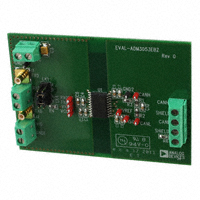
EVAL–ADM3053EBZ evaluation board
DOCUMENTS NEEDED
ADM3053 data sheet
09833-001
EVAL-ADM3053EBZ EVALUATION BOARD PHOTOGRAPH
Figure 1.
PLEASE SEE THE LAST PAGE FOR AN IMPORTANT
WARNING AND LEGAL TERMS AND CONDITIONS.
Rev. A | Page 1 of 10
�UG-234
EVAL-ADM3053EBZ User Guide
TABLE OF CONTENTS
Features .............................................................................................. 1
Overlapping Stitching Capacitor .................................................4
Evaluation Kit Contents ................................................................... 1
PCB Layout Reccomendations ....................................................4
Documents Needed .......................................................................... 1
EN55022 Radiated Emissions Test Results ................................4
General Description ......................................................................... 1
Evaluation Board Schematics and Artwork ...................................6
EVAL-ADM3053EBZ Evaluation Board Photograph ................. 1
Ordering Information .......................................................................9
Revision History ............................................................................... 2
Bill of Materials ..............................................................................9
Evaluation Board Hardware ............................................................ 3
Related Links ......................................................................................9
Setting Up the Evaluation Board ................................................ 3
REVISION HISTORY
7/2017—Rev. 0 to Rev. A
Deleted ADM3053 Applications Section, Equipment Needed
Section, and Functional Block Diagram Section.......................... 1
Changes to Features Section and Figure 1..................................... 1
Added Evaluation Kit Contents Section, Documents Needed
Section, and Evaluation Board Photograph Section .................... 1
Changes to Setting Up the Evaluation Board Section and
Figure 3 .............................................................................................. 3
Added Table 1, Renumbered Sequentially .................................... 3
Added Overlapping Stitching Capacitors Section, PCB Layout
Recommendations Section, EN55022 Radiated Emissions Test
Results Section, and Figure 4; Renumbered Sequentially ............ 4
Added Figure 5, Figure 6, and Table 2 ............................................5
Changes to Figure 7 ...........................................................................6
Deleted Figure 9 and Figure 10........................................................6
Changes to Figure 8 and Figure 10..................................................7
Added to Figure 9 ..............................................................................7
Changes to Figure 11, Figure 12, and Figure 13 ............................8
Changes to Table 3 and Related Links Section ..............................9
7/2011—Revision 0: Initial Version
Rev. A | Page 2 of 10
�EVAL-ADM3053EBZ User Guide
UG-234
EVALUATION BOARD HARDWARE
boards together, replace these values with 60 Ω + 60 Ω, or if
connecting one board to a double terminated bus, remove both
resistors (R5 and R6 not fitted). Table 1 shows parameters set by
the on-board resistors.
SETTING UP THE EVALUATION BOARD
The EVAL-ADM3053EBZ evaluation board default configuration
is shown in Figure 3. In the default configuration, R2 is fitted
with a 0 Ω resistor, and R3 is open, which allows VIO to be
powered by 3.3 V or 5 V on J4, corresponding to the logic levels
required for TXD and RXD. A power supply with a voltage of
6 V to 9 V is required on the input supply, Pin 8 (IN) of the onboard low dropout regulator, LDO (VCC on J5). The on-board
LDO generates the required 5 V to the ADM3053 VCC pin. By
fitting R3 with a 0 Ω resistor and removing R2, VIO of the EVALADM3053EBZ is connected to the ADM3053 VCC pin, and the
complete board can be powered by a 9 V battery (for example,
for electromagnetic current (EMC) testing).
Figure 3 shows an example operation of the EVAL–ADM3053EBZ.
Connect a clock generator on TXD and set up a 500 kHz square
wave clock with the output swinging between 0 V and 5 V. Connect
the scope probes to the test points: TXD, RXD, CANH, and
CANL. Figure 2 shows an example oscilloscope plot; Channel 1
shows the TXD signal, and Channel 2 and Channel 3 show the
CANH and CANL signals.
TEK STOP: 50.0MS/s
VCC supplies power to the isoPower circuitry, and VIO supplies
the iCoupler circuitry. Decoupling capacitors of values 0.1 μF
and 10 μF are fitted to C3 and C4 between VCC and GND1 and
of values 0.01 μF and 0.1 μF to C1 and C2 between VIO and GND1.
On the bus side, it is required that VISOIN connect to VISOOUT. A
10 μF reservoir capacitor (C8) and a 0.1 μF decoupling capacitor
(C7) are fitted between VISOOUT and GND2. Two 0.1 μF and
0.01 μF decoupling capacitors (C5 and C6) are fitted between
VISOIN and GND2.
1
J1
RXD
J2
TXD
RXD
R2 R3
3.3V OR 5V
POWER
SUPPLY
VIO
GND1
GND2
M 1.00µs
CH1
1.20V
Figure 2. ADM3053 TXD, CANH, and CANL Signals
GND2
VREF CANH
CANL
VIO
VCC
VISO SHIELD
VCC
(VIN)
J5
J6
OSCILLOSCOPE
EVAL-ADM3053EBZ
Rev B
09833-001
J4
CH2 2.00V
GND1
TXD
J3
CH1 2.00V
CH3 2.00V
09833-002
3 2
Resistor R4 connects the ADM3053 RS pin to GND2 to adjust
the slope of the CANH and CANL signals, as required. Resistor R4,
by default, is a 0 Ω resistor for full speed operation. Replacing
R4 with a 47 kΩ resistor (or similar) limits the slew rate of the
CANH and CANL signals. By default, the R5 and R6 resistors
load the ADM3053 CANH pin and CANL pin with 60 Ω (30 Ω
+ 30 Ω) to simulate a double terminated bus. If connecting two
SIGNAL
GENERATOR
136 ACQS
6V TO 9V
POWER SUPPLY
Figure 3. Basic Isolated CAN Transceiver Evaluation Board Operation
Table 1. Parameters Set by On-Board Resistors
Resistor(s)
R2, R3
R4
R5, R6
Values
0 Ω for R2, R3 not fitted
R2 not fitted, 0 Ω for R3
0Ω
47 kΩ
Both 30 Ω
Both 60 Ω
Both not fitted
Default
Yes
No
Yes
No
Yes
No
No
Test Conditions/Comments
VIO connected to J4
VIO connected to the ADM3053 VCC/5 V LDO output (J4 VIO unconnected)
ADM3053 in full speed mode
ADM3053 in slope control mode
Simulates double terminated bus
Allows another node with 120 Ω termination to be connected
Allows a double terminated bus to be connected
Rev. A | Page 3 of 10
�UG-234
EVAL-ADM3053EBZ User Guide
OVERLAPPING STITCHING CAPACITOR
The evaluation board implements an embedded stitching
capacitor structure. A printed circuit board (PCB) embedded
stitching capacitor is created when two metal planes in a PCB
overlap each other and are separated by dielectric material. This
overlap is formed by extending the internal reference planes
from the primary and secondary layers across the area that is
used for creepage on the PCB surface. This capacitor provides a
return path for high frequency common-mode noise currents
across the isolation gap. The overlapping area is 24.9 mm ×
6.3 mm, the distance between overlapping layers is ~0.7 mm;
therefore, the plate capacitor is around 8.9 pF. For full details on
the layout and implementation of embedded stitching capacitors,
see the AN-0971 Application Note, Recommendations for
Control of Radiated Emissions with isoPower Devices.
Ensure that there is a keep out area in the PCB layout
around the L1 and L2 ferrites (no PCB planes under or
alongside L1 and L2).
The ADM3053 evaluation board reduces emissions generated
by the high frequency switching elements used by the isoPower
technology to transfer power through the integrated isolated
dc-to-dc power supply. The layout of the evaluation board is
generated using guidelines similar to those in the AN-1349
Application Note, PCB Implementation Guidelines to Minimize
Radiated Emissions on the ADM2582E/ADM2587E RS-485/
RS-422 Transceivers.
09833-004
PCB LAYOUT RECCOMENDATIONS
Figure 4. Layout Notes for EVAL-ADM3053EBZ
To pass EN55022 Class B on a 4-layer PCB, the following layout
guidelines are recommended:
Best practice decoupling on the PCB per the ADM3053
data sheet.
Place ferrite beads between the PCB trace/plane connections
and the ADM3053 VISOOUT pin (Pin 12) and GND2 pins
(Pin 11 and Pin 13).
Do not connect the VISOOUT pin to a power plane; connect
between the VISOOUT pin and the VISOIN pin using a PCB
trace. Ensure VISOOUT (Pin 12) is connected first through
the L1 ferrite before connecting to VISOIN (Pin 19), as shown
in Figure 4.
An embedded stitching capacitor between the GND1 PCB
plane and GND2 Pin 11 and Pin 13 (inside L2 ferrite)
using internal layers of the PCB planes as highlighted in
the area around U1 in Figure 4 (see the Overlapping
Stitching Capacitor section).
The following additional notes apply to the PCB layout; refer to
the schematic and artwork in Figure 7 to Figure 13.
Ensure that GND2 (Pin 13) is connected to GND2 (Pin 11)
on the inside (device side) of the C7 100 nF capacitor.
Ensure that the C7 capacitor is connected between VISOOUT
(Pin 12) and GND2 (Pin 11) on the device side of the L1
and L2 ferrite beads.
Ensure that GND2 (Pin 16) is connected to the main bus
side PCB ground plane outside of the L2 ferrite, as shown
in Figure 4.
Locate the power delivery circuit in close proximity to the
ADM3053 device, to ensure that the VCC trace is as short as
possible. The EVAL-ADM3053EBZ PCB has a power
delivery circuit located at the bottom of the PCB with a
short trace from the ADP667ARZ regulator output (U3) to
VCC (Pin 8). This layout example minimizes the loop area
in which high frequency current can flow. An increase in
the loop area results in an increase in the emissions levels.
EN55022 RADIATED EMISSIONS TEST RESULTS
The EVAL-ADM3053EBZ evaluation board is tested and
certified to pass EN55022 Class B with a 2.48 dB μV/m margin.
EN55022 certification documents for the EVAL-ADM3053EBZ
evaluation board is available to users upon request from Analog
Devices. Table 2 provides a summary of the results. All EN55022
radiated emissions tests are performed with the PCB schematic
and layout as described in Figure 7 to Figure 13.
The EVAL-ADM3053EBZ evaluation boards are configured and
tested with 5.0 V power supplied to the ADM3053 VIO pin and
VCC pin, with the power supplied from the ADP667ARZ
regulator output. The ADP667ARZ regulator input is supplied
from a standard 9 V battery. Testing is performed with an active
500 kbps clock on the TXD pin supplied by an on-board oscillator
fitted to U2. The ADM3053 CAN bus pins are loaded with a 60 Ω
termination resistor (per a double terminated bus). Measurements
are carried out in an anechoic chamber at 10 m from 30 MHz to
3 GHz. Figure 5 and Figure 6 show the results of the peak
horizontal and vertical scans, and Table 2 shows the tabulated
quasi-peak (QP) results.
Rev. A | Page 4 of 10
�UG-234
80
80
70
70
PEAK EMISSIONS (dBµV/m)
60
50
EN55022 CLASS A LIMIT
40
30
EN55022 CLASS B LIMIT
20
50
40
30
EN55022 CLASS A LIMIT
EN55022 CLASS B LIMIT
20
10
0
30
100
1000
FREQUENCY (MHz)
09833-005
10
60
Figure 5. Horizontal Scan From 30 MHz to 1000 MHz
0
30
100
1000
FREQUENCY (MHz)
09833-006
PEAK EMISSIONS (dBµV/m)
EVAL-ADM3053EBZ User Guide
Figure 6. Vertical Scan from 30 MHz to 1000 GHz
Table 2. ADM3053 Test Results (Quasi-Peak Measurements)
Frequency (MHz)
182.330
364.902
182.027
364.058
QP Level dB (μV/m)
17.5
31.9
12.0
22.1
EN55022 Class B dB (μV/m)
30
37
30
37
Rev. A | Page 5 of 10
Antenna Position
Horizontal
Horizontal
Vertical
Vertical
Antenna Height (m)
4.00
2.50
1.00
1.50
Pass/Fail
Pass
Pass
Pass
Pass
�UG-234
EVAL-ADM3053EBZ User Guide
EVALUATION BOARD SCHEMATICS AND ARTWORK
09833-007
Figure 7. EVAL-ADM3053EBZ Evaluation Board Schematic
Rev. A | Page 6 of 10
�UG-234
09833-008
EVAL-ADM3053EBZ User Guide
09833-009
Figure 8. EVAL-ADM3053EBZ Evaluation Board Silkscreen (Top)
09833-010
Figure 9. EVAL-ADM3053EBZ Evaluation Board Silkscreen (Bottom)
Figure 10. EVAL-ADM3053EBZ Evaluation Board Component Side
Rev. A | Page 7 of 10
�EVAL-ADM3053EBZ User Guide
09833-011
UG-234
09833-012
Figure 11. EVAL-ADM3053EBZ Evaluation Board Layer 2
09833-013
Figure 12. EVAL-ADM3053EBZ Evaluation Board Layer 3
Figure 13. EVAL-ADM3053EBZ Evaluation Board Solder Side
Rev. A | Page 8 of 10
�EVAL-ADM3053EBZ User Guide
UG-234
ORDERING INFORMATION
BILL OF MATERIALS
Table 3.
Quantity
2
6
2
1
2
1
3
2
1
2
1
1
1
1
2
5
2
3
1
Name
C1, C5
C2, C3, C6, C7, C11, C12
C4, C8
C9
C10, C13
C14 (not placed)
J1, J4, J5
J2, J3
J6
L1, L2
R1 (not placed)
R2, R7
R3 (not placed)
R4
R5, R6
CANH, CANL, RXD, TXD, VREF
GND1, GND2
VCC, VIO, VISO
U1
1
U2
1
U3 (not placed)
Description
Capacitor, X7R, 10 nF, 0603
Capacitor, X7R, 100 nF, 0603
Capacitor, X7R, 10 µF, 0805
Capacitor, X7R, 47 nF, 0603
Capacitor, tantalum, 10 µF, Case C
Capacitor, X7R, 100 nF (optional)
2-pin terminal block
SMA, straight jack
4-pin terminal block
Ferrite bead, 1.8 kΩ at 100 MHz
Resistor, 402 kΩ, 0603 (optional)
Resistor, 0 Ω, 0805
Resistor, 0 Ω, 0805 (optional)
Resistor, 0 Ω, 0603
Resistor, thick film, 30 Ω, 0.5 W, 0805
Test point, yellow
Test point, black
Test point, red
ADM3053 isolated CAN transceiver with
isoPower integrated dc-to-dc converter
5 V fixed, adjustable low dropout linear
voltage regulator
Oscillator, 1 kHz to 20 MHz (optional)
Supplier
Multicomp
Multicomp
AVX
Multicomp
Kemet
Multicomp
Lumberg
TE Connectivity
Lumberg
Murata
Multicomp
Vishay Draloric
Vishay Draloric
Multicomp
Panasonic
Vero
Vero
Vero
Analog Devices
Part No.
MC0603B103K160CT
MC0603B104K160CT
0805ZC106KAT2A
MC0603B473K500CT
B45196E3106K309
MC0603B104K160CT
KRM 02
5-1814832-1
KRM 04
BLM15HD182SN1D
MC0063W06031402K
CRCW08050000ZSTA
CRCW08050000ZSTA
MC0063W06030R
ERJP06F30R0V
20-313140
20-2137
20-313137
ADM3053BRWZ
Analog Devices
ADP667ARZ
Linear Technology
LTC6900CS5#TRMPBF
RELATED LINKS
Resource
ADM3053
AN-1349
AN-1123
AN-0971
Description
Signal and Power isolated CAN Transceiver with Integrated Isolated DC-to-DC Converter
PCB Implementation Guidelines to Minimize Radiated Emissions on the ADM2582E/ADM2587E RS-485/RS-422 Transceivers
Controller Area Network (CAN) Implementation Guide
Recommendations for Control of Radiated Emissions with isoPower Devices
Rev. A | Page 9 of 10
�UG-234
EVAL-ADM3053EBZ User Guide
NOTES
ESD Caution
ESD (electrostatic discharge) sensitive device. Charged devices and circuit boards can discharge without detection. Although this product features patented or proprietary protection
circuitry, damage may occur on devices subjected to high energy ESD. Therefore, proper ESD precautions should be taken to avoid performance degradation or loss of functionality.
Legal Terms and Conditions
By using the evaluation board discussed herein (together with any tools, components documentation or support materials, the “Evaluation Board”), you are agreeing to be bound by the terms and conditions
set forth below (“Agreement”) unless you have purchased the Evaluation Board, in which case the Analog Devices Standard Terms and Conditions of Sale shall govern. Do not use the Evaluation Board until you
have read and agreed to the Agreement. Your use of the Evaluation Board shall signify your acceptance of the Agreement. This Agreement is made by and between you (“Customer”) and Analog Devices, Inc.
(“ADI”), with its principal place of business at One Technology Way, Norwood, MA 02062, USA. Subject to the terms and conditions of the Agreement, ADI hereby grants to Customer a free, limited, personal,
temporary, non-exclusive, non-sublicensable, non-transferable license to use the Evaluation Board FOR EVALUATION PURPOSES ONLY. Customer understands and agrees that the Evaluation Board is provided
for the sole and exclusive purpose referenced above, and agrees not to use the Evaluation Board for any other purpose. Furthermore, the license granted is expressly made subject to the following additional
limitations: Customer shall not (i) rent, lease, display, sell, transfer, assign, sublicense, or distribute the Evaluation Board; and (ii) permit any Third Party to access the Evaluation Board. As used herein, the term
“Third Party” includes any entity other than ADI, Customer, their employees, affiliates and in-house consultants. The Evaluation Board is NOT sold to Customer; all rights not expressly granted herein, including
ownership of the Evaluation Board, are reserved by ADI. CONFIDENTIALITY. This Agreement and the Evaluation Board shall all be considered the confidential and proprietary information of ADI. Customer may
not disclose or transfer any portion of the Evaluation Board to any other party for any reason. Upon discontinuation of use of the Evaluation Board or termination of this Agreement, Customer agrees to
promptly return the Evaluation Board to ADI. ADDITIONAL RESTRICTIONS. Customer may not disassemble, decompile or reverse engineer chips on the Evaluation Board. Customer shall inform ADI of any
occurred damages or any modifications or alterations it makes to the Evaluation Board, including but not limited to soldering or any other activity that affects the material content of the Evaluation Board.
Modifications to the Evaluation Board must comply with applicable law, including but not limited to the RoHS Directive. TERMINATION. ADI may terminate this Agreement at any time upon giving written notice
to Customer. Customer agrees to return to ADI the Evaluation Board at that time. LIMITATION OF LIABILITY. THE EVALUATION BOARD PROVIDED HEREUNDER IS PROVIDED “AS IS” AND ADI MAKES NO
WARRANTIES OR REPRESENTATIONS OF ANY KIND WITH RESPECT TO IT. ADI SPECIFICALLY DISCLAIMS ANY REPRESENTATIONS, ENDORSEMENTS, GUARANTEES, OR WARRANTIES, EXPRESS OR IMPLIED, RELATED
TO THE EVALUATION BOARD INCLUDING, BUT NOT LIMITED TO, THE IMPLIED WARRANTY OF MERCHANTABILITY, TITLE, FITNESS FOR A PARTICULAR PURPOSE OR NONINFRINGEMENT OF INTELLECTUAL
PROPERTY RIGHTS. IN NO EVENT WILL ADI AND ITS LICENSORS BE LIABLE FOR ANY INCIDENTAL, SPECIAL, INDIRECT, OR CONSEQUENTIAL DAMAGES RESULTING FROM CUSTOMER’S POSSESSION OR USE OF
THE EVALUATION BOARD, INCLUDING BUT NOT LIMITED TO LOST PROFITS, DELAY COSTS, LABOR COSTS OR LOSS OF GOODWILL. ADI’S TOTAL LIABILITY FROM ANY AND ALL CAUSES SHALL BE LIMITED TO THE
AMOUNT OF ONE HUNDRED US DOLLARS ($100.00). EXPORT. Customer agrees that it will not directly or indirectly export the Evaluation Board to another country, and that it will comply with all applicable
United States federal laws and regulations relating to exports. GOVERNING LAW. This Agreement shall be governed by and construed in accordance with the substantive laws of the Commonwealth of
Massachusetts (excluding conflict of law rules). Any legal action regarding this Agreement will be heard in the state or federal courts having jurisdiction in Suffolk County, Massachusetts, and Customer hereby
submits to the personal jurisdiction and venue of such courts. The United Nations Convention on Contracts for the International Sale of Goods shall not apply to this Agreement and is expressly disclaimed.
©2011–2017 Analog Devices, Inc. All rights reserved. Trademarks and
registered trademarks are the property of their respective owners.
UG09833-0-7/17(A)
Rev. A | Page 10 of 10
�