EVAL-ADuCM350EBZ User Guide
UG-668
One Technology Way • P.O. Box 9106 • Norwood, MA 02062-9106, U.S.A. • Tel: 781.329.4700 • Fax: 781.461.3113 • www.analog.com
Evaluating the ADuCM350 16-Bit, Precision, Low Power Meter-on-a-Chip
FEATURES
ADDITIONAL EQUIPMENT AND SOFTWARE NEEDED
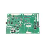
ADuCM350 motherboard
Selection of daughter boards for analog front end and
platform validation
3 power supply options: 2.5 V to 3.6 V from an external
power supply, 5 V from interface/emulator board, or
CR2032 battery connection
Interface options
UART and serial wire through 8-pin J-Link OB connector
Trace capability
Power indicator/general-purpose LEDs
Reset, download, and external interrupt push-buttons
Supercapacitor and thermistor capability
USB connectivity
8-pin connector to the interface/emulator board
Access to ADuCM350 platform pins through Digital Header 1,
Digital Header2, and CapTouch header
32.768 kHz external crystal and 16 MHz external crystal
Evaluation software for the ADuCM350 (download from the
ADuCM350 design resources page)
Extra peripheral boards available for order: Ev-ADuCM350AUDZ,
Ev-ADuCM350DISZ
See the ADuCM350 design resources page for more details
EVALUATION KIT CONTENTS
EVAL-ADuCM350EBZ board
USB-SWD/UART-EMUZ, also known as J-Link OB emulator
AFE daughter boards: ADuCM350 switch mux configuration
board, ADuCM350 4-wire bio Configuration 2 board
ADuCM350 breakout board
ADuCM350 GPIO test header board
USB cable
SYSTEM REQUIREMENTS
Minimum requirement to run examples and applications
PC with USB 2.0 controller connection and 1 free COM port
Windows XP SP3 or later, Windows Vista, or Windows 7 or later
ONLINE RESOURCES
Documents Needed
ADuCM350 data sheet
ADuCM350 hardware reference manual
AN-1262, AN-1263, AN-1271, AN-1281, AN-1286,
AN-1293, AN-1302 application notes
ADuCM350 software development kit quick start guide
(UG-677)
Required Software
ADuCM350 software development kit (firmware/debug
environment)
IAR Embedded Workbench for ARM (from Version 7.10+)
ADuCM350 evaluation kit software platform (GUI software)
Design and Integration Files
Schematics, layout files, bill of materials
TYPICAL SETUP
PERIPHERALS
CONNECTOR
2
PERIPHERALS
CONNECTOR
1
USB
CapTouch
CONNECTOR
USB-SWD/UART-EMUZ
TRACE
CR2032
EXTERNAL
SUPPLY SUPPLY
Figure 1. Typical Setup (USB-SWD/UART-EMUZ on Left and EVAL-ADuCM350EBZ on Right)
PLEASE SEE THE LAST PAGE FOR AN IMPORTANT
WARNING AND LEGAL TERMS AND CONDITIONS.
Rev. A | Page 1 of 28
12104-001
AFE
DAUGHTER
BOARD
�UG-668
EVAL-ADuCM350EBZ User Guide
TABLE OF CONTENTS
Features .............................................................................................. 1
Jumper Settings ..................................................................................6
Evaluation Kit Contents ................................................................... 1
Evaluation Board Circuitry ..............................................................7
Additional Equipment and Software Needed................................... 1
J-Link OB Emulator ......................................................................7
System Requirements ....................................................................... 1
Digital Header Pad Lookup Table ...............................................8
Online Resources .............................................................................. 1
ADuCM350 Motherboard Schematics ...........................................9
Typical Setup ..................................................................................... 1
ADuCM350 Daughter Board Schematics ................................... 16
Revision History ............................................................................... 2
ADuCM350 Switch Mux Configuration Board ..................... 16
General Description ......................................................................... 3
ADuCM350 4-Wire Bio Configuration 2 Board ................... 18
Getting Started .................................................................................. 4
Audio Daughter Board Reference Schematics ....................... 20
Software Installation Procedures ................................................ 4
Display Board Reference Schematics ....................................... 22
Evaluation Board Setup Procedures........................................... 4
Breakout Board Pin Connections ............................................ 25
Evaluation Board Hardware ............................................................ 5
GPIO Test Header Board........................................................... 26
Power Supplies .............................................................................. 5
Limitations on Use and Liability .................................................. 28
REVISION HISTORY
1/2018—Rev. 0 to Rev. A
Added Limitations on Use and Liability Section........................ 28
5/2014—Revision 0: Initial Version
Rev. A | Page 2 of 28
�EVAL-ADuCM350EBZ User Guide
UG-668
GENERAL DESCRIPTION
The ADuCM350 is a 16 MHz ARM® Cortex-M3 processor with
a high precision AFE specifically designed for high precision
data acquisition.
The ADuCM350 has a 16-bit precision analog core with four
dedicated voltage measurement channels and up to eight current
measurement channels. It has an integrated complex impedance
measurement system and uses an integrated parameterizable
waveform generator to generate complex waveforms. It uses an
excitation amplifier control loop to perform accurate potentiostat
type measurements and has a highly configurable switch matrix
that allows application specific amplifier configuration.
The EVAL-ADuCM350EBZ kit provides scientists, system
analyzers, and software developers a platform to migrate from
sensor investigation and analysis to full ecosystem development.
The evaluation kit consists of an ADuCM350 motherboard and a
selection of analog front end and digital peripheral daughter boards.
The evaluation kit is designed specifically to work with the
ADuCM350 software development kit (SDK) and the evaluation
kit support package (EKSP)—both of which are available for
download on the ADuCM350 design resources page.
The software development kit is designed to work with the IAR
debugging environment only. The user guide for the ADuCM350
SDK is available on the SDK installer.
The device has a large array of peripherals, including USB,
CapTouch®, display, audio, and an array of serial interfaces
and GPIOs.
An example of where the kit is downloaded follows: C:\Analog
Devices\ADuCM350BBCZ\Eval-ADUCM350EBZ\doc
The ADuCM350 includes 384 kB of flash, 32 kB of SRAM, and
16 kB of flash configured as EEPROM.
The SDK quick start guide and the EKSP user guide are available in
the Support Documentation zipped folder.
Rev. A | Page 3 of 28
�UG-668
EVAL-ADuCM350EBZ User Guide
GETTING STARTED
SOFTWARE INSTALLATION PROCEDURES
EVALUATION BOARD SETUP PROCEDURES
For software installation procedures, refer to the following
ADuCM350 software documentation for further details:
1.
Plug the ADuCM350 switch mux configuration board into
the ADuCM350 evaluation board, EVAL-ADuCM350EBZ.
•
2.
Plug the USB-SWD/UART-EMUZ board into J14 on the
ADuCM350 evaluation board, EVAL-ADuCM350EBZ.
3.
Plug the USB cable into the USB-SWD/UART-EMUZ board.
After the drivers are downloaded, you can begin communicating
with the board.
12104-003
•
For more information about the EKSP LabVIEW® GUI,
refer to the EKSP user guide (ADuCM350_Evaluation_Kit_
Software_Platform.pdf) within the Documentation
folder of the software development kit.
For more information about the SDK firmware/debug
environment, refer to SDK user guide (ADuCM350BBCZ_
Software_Users_Guide.pdf) within the Documentation
folder of the software development kit and to the ADuCM350
software development kit quick start guide, UG-677.
Figure 2. EVAL-ADuCM350EBZ Setup
Rev. A | Page 4 of 28
�EVAL-ADuCM350EBZ User Guide
UG-668
EVALUATION BOARD HARDWARE
POWER SUPPLIES
VDD_IO
VCCM_ANA
Table 2 describes the two options for supplying power to the
VDD_IO pin.
Table 1 describes the three options for supplying power to the
VCCM_ANA pin.
Link M5 Position
A (Default Position)
B
Table 1. VCCM_ANA Supply Options
Link J10 Position
A (Default Position)
VCCM_ANA Supply
Regulated 3.3 V from J3 wall socket
supplied with board
CR2032 battery connection, J19
External supply
VDD_IO Supply
From VCCM_ANA
Regulated 3.3 V from J3 wall socket
(supplied with board)
VLCDVDD
Table 3 describes the three options for supplying power to the
VLCDVDD pin.
Table 3. VLCDVDD Supply Options
LK14 Position 1
Inserted
Open
1
VLCDVDD Supply
Powered by VCCM
Not powered
The default position for LK14 is to be removed.
3.3V_BOARD
OPTION 1
T68
U6
2 IN
5V_USB
+
OUT 1
SD GND
3
7
C37
10uF
R32
L2
R31
0r
BEAD
1r6
LK5
VDDOUT
R30
560r
D4
POWER
OPTION 2
USB REGULATOR
LK24
T3
VUSB
J10
A
B
VCCM_ANA
C
+
J19
BATT-3002-20MM
BATTERY CONTACT
LK10
OPTION 3
J12-2
C34
0.1uF
C40
10uF
J12-1
12104-002
B
C
Table 2. VDD_IO Supply Options
NOTES
1. LK24 IS NOT INSERTED BY DEFAULT.
Figure 3. Power Supply Schematic for VCCM_ANA Pin
Rev. A | Page 5 of 28
�UG-668
EVAL-ADuCM350EBZ User Guide
JUMPER SETTINGS
Table 4. Link Option Functions
Link Number
LK1
LK2
LK3
LK4
LK6
LK7
LK8
LK9
LK10
LK11
LK12
LK13
LK14
LK24
M1
M2
M3
M5
Default Position
Short
Open
Open
Short
Open
Open
Short
Open
Short
Open
Short
Short
Open
Open
B
B
Open
A
Function
AN_A to AFE daughter board.
LED GPIO functionality of P2.1.
AN_B to AFE daughter board.
Connect the supercapacitor to the VBACK pin.
Thermistor voltage output measurement (AN_A).
VCCM_DIG to VCCM_ANA external connection (connected internally on chip).
LED GPIO functionality of P0.11.
AN_C to AFE daughter board.
AGND To DGND connector.
AN_D to AFE daughter board.
LED GPIO functionality of P4.2.
VBUS link.
Supply for VLCDVDD.
VUSB to VCCM_ANA connector. The battery must be removed when this link is inserted.
P0.6 selected for UART Tx.
P0.7 selected For UART Rx.
AN_EXCITE used for thermistor operation.
VDD_IO connection. When this link is in Position A, the VDD_IO supply is from
VCCM_ANA.
Rev. A | Page 6 of 28
�EVAL-ADuCM350EBZ User Guide
UG-668
TO EVALUATION BOARD CONNECTOR
J-LINK OB EMULATOR
The J-Link OB emulator provides nonintrusive emulation via a
serial wire and allows supply and UART communication with
the ADuCM350 evaluation board (EVAL-ADuCM350EBZ).
Figure 4 shows a top view of the emulator board. The J2
connector plugs into the ADuCM350 evaluation board (EVALADuCM350EBZ). The J2 connector pinout is shown in Figure 5.
12104-105
EVALUATION BOARD CIRCUITRY
Figure 5. J2 Connector
12104-104
For downloading and debugging, LK1, LK2, LK4, and LK6 must
be inserted. LK3 and LK5 are required to communicate via
UART. The required driver software for the J-Link OB can be
downloaded from the Segger website. Ensure that you also
install the virtual COM port drivers (see Figure 6).
12104-106
Figure 4. Emulator Top View
Figure 6. J-Link OB Download Options
Rev. A | Page 7 of 28
�UG-668
EVAL-ADuCM350EBZ User Guide
DIGITAL HEADER PAD LOOKUP TABLE
Table 5. Pinout for Digital Header 1 Pad (J20) on EVAL-ADuCM350EBZ
Pin No.
J20-2
J20-4
J20-6
J20-8
J20-10
J20-12
J20-14
J20-16
J20-18
J20-20
J20-22
J20-24
J20-26
J20-28
J20-30
J20-32
J20-34
J20-36
J20-38
J20-40
J20-42
J20-44
J20-46
J20-48
J20-50
Top Row (from Left to Right)
Internal Connection
P2.1
P2.3
P2.5
P1.0
P1.2
P1.4
P1.6
P3.8
P3.3
P1.11
P1.13
P1.15
P2.11
P2.12
P2.15
P3.10
P2.13
P3.11
P3.0
P3.1
P3.5
P3.7
N/A
N/A
N/A
Pin No.
J20-1
J20-3
J20-5
J20-7
J20-9
J20-11
J20-13
J20-15
J20-17
J20-19
J20-21
J20-23
J20-25
J20-27
J20-29
J20-31
J20-33
J20-35
J20-37
J20-39
J20-41
J20-43
J20-45
J20-47
J20-49
Bottom Row (from Left to Right)
Internal Connection
P2.0
P2.2
P2.4
P1.1
P1.3
P1.5
P1.7
P1.9
P3.9
P1.8
P1.10
P1.12
P1.14
P2.10
P2.9
P2.8
P2.7
P2.6
P2.14
P3.2
P3.4
P3.6
N/A
N/A
N/A
Table 6. Pinout for Digital Header 2 Pad (J5) on EVAL-ADuCM350EBZ
Pin No.
J5-19
J5-17
J5-15
J5-13
J5-11
J5-9
J5-7
J5-5
J5-3
J5-1
Top Row (from Left to Right)
Internal Connection
N/A
N/A
N/A
N/A
P0.14
P0.12
P1.0
P4.1
P3.14
P3.12
Pin No.
J5-20
J5-18
J5-16
J5-14
J5-12
J5-10
J5-8
J5-6
J5-4
J5-2
Rev. A | Page 8 of 28
Bottom Row (from Left to Right)
Internal Connection
N/A
N/A
N/A
N/A
P0.15
P0.13
P0.11
P4.2
P4.0
P3.13
�EVAL-ADuCM350EBZ User Guide
UG-668
VLCD_VDD
VLCD_13
VLCD_23
VLCD_FLY2
VLCD_FLY1
ADUCM350 MOTHERBOARD SCHEMATICS
D2
C2
B1
F2
E2
P2.0
P2.1
P2.2
P2.3
P2.4
P2.5
P2.6
P2.7
P2.8
P2.9
P2.10
P2.11
P2.12
P2.13
P2.14
P2.15
AN_A
AN_B
AN_C
AN_D
TRST
TRACECLK
TRACEDATA0
TRACEDATA1
TRACEDATA2
TRACEDATA3
P3.0
P3.1
P3.2
P3.3
P3.4
P3.5
P3.6
P3.7
P3.8
P3.9
P3.10
P3.11
P3.12
P3.13
P3.14
K10
AGND_REF
P14
AGND_CTOUCH
R4
AVDD_TX/RX
K9
AGND_TX/RX
P4
HF_XTAL1
HF_XTAL2
AVDD_TX/RX
VCCM_ANA
RTC_XTAL2
RTC_XTAL1
VCCM_ANA
L1
P4.0
L2
P4.1
R1 P4.2
VUSB
DGND_USB
VBUS
USB_DM
USB_DP
Figure 7. ADuCM350 Motherboard Schematic Device Drawing
Rev. A | Page 9 of 28
N2
A1
K8
KERNEL_GPIO
R10
P10
VREF
VBIAS
P5
R5
RCAL1
RCAL2
R6
P6
R7
P7
R8
P8
R9
P9
AFE1
AFE2
AFE3
AFE4
AFE5
AFE6
AFE7
AFE8
P11
R11
TIA_I
TIA_O
R12
REF_EXCITE
P12
P13
R13
R14
AN_A
AN_B
AN_C
AN_D
R15
M15
M14
N15
N14
P15
TRST
TRACECLK
TRACEDATA0
TRACEDATA1
TRACEDATA2
TRACEDATA3
E1
F6
G2
F1
G1
VUSB
N1
P1
RTC_XTAL2
RTC_XTAL1
D1
C1
HF_XTAL1
HF_XTAL2
RESETX
VBUS
USB_DM
USB_DP
12104-107
REF_EXCITE
H6 VCCM_DIG
P4.0
P4.1
P4.2
TIA_I
TIA_O
VCCM_DIG
F14
G14
F15
F10
G10
H10
G15
J10
F8
F9
C14
E14
K6
K7
J6
AFE1
AFE2
AFE3
AFE4
AFE5
AFE6
AFE7
AFE8
DVDD
P3.0
P3.1
P3.2
P3.3
P3.4
P3.5
P3.6
P3.7
P3.8
P3.9
P3.10
P3.11
P3.12
P3.13
P3.14
P1.0
P1.1
P1.2
P1.3
P1.4
P1.5
P1.6
P1.7
P1.8
P1.9
P1.10
P1.11
P1.12
P1.13
P1.14
P1.15
VBACK
VDD_IO
B2
A2
B3
A3
B4
A4
D15
C15
B15
A14
A13
B13
B14
D14
E15
A15
RCAL1
RCAL2
K1
P2.0
P2.1
P2.2
P2.3
P2.4
P2.5
P2.6
P2.7
P2.8
P2.9
P2.10
P2.11
P2.12
P2.13
P2.14
P2.15
VREF
VBIAS
M1
VBACK
H15
VDD_IO
A5
B5
A6
B6
A7
B7
A8
B8
A9
B9
A10
B10
A11
B11
A12
B12
KERNEL_GPIO
APLATFORM_TEST
RESETX
ADUCM350-OM
DVDD
P1.0
P1.1
P1.2
P1.3
P1.4
P1.5
P1.6
P1.7
P1.8
P1.9
P1.10
P1.11
P1.12
P1.13
P1.14
P1.15
U1
P0.0
P0.1
P0.2
P0.3
P0.4
P0.5
P0.6
P0.7
P0.8
P0.9
P0.10
P0.11
P0.12
P0.13
P0.14
P0.15
VLCD_VDD
VLCD_13
VLCD_23
VLCD_FLY2
VLCD_FLY1
K15
J15
L15
K14
J14
L14
J1
J2
H1
H2
R2
K2
R3
P2
P3
M2
H14
DGND
G6
F7 DGND1
DGND2
P0.0
P0.1
P0.2
P0.3
P0.4
P0.5
P0.6
P0.7
P0.8
P0.9
P0.10
P0.11
P0.12
P0.13
P0.14
P0.15
ADuCM350
�UG-668
EVAL-ADuCM350EBZ User Guide
LF 32kHz XTAL
HF 16MHz XTAL
P2.1
LK2
DISPLAY2
R60
560r
HF_XTAL1
C7
VCCM_DIG
LK8
P0.11
DISPLAY
R2
560r
LED-0603-RED
3.3V_BOARD
LED-0603-RED
HF_XTAL2
RTC_XTAL1
15pF
Y3
1
Y1
2
C2
C8
3
GND
GND
P3.6
560r
DNI
XTAL-FA238
3.3V_BOARD
LK12
P4.2
DISPLAY1
R59
560r
LED-0603-RED
3.3V_BOARD
LED-0603-RED
C4
24pF
RTC_XTAL2
DISPLAY3
R61
R62
4
24pF
15pF
GPIO LEDs
Layout: Needs To Be Near DUT
Layout: Shielding on 16MHz
EXT INT
P0.10
P3.4
VLCD_VDD
T4
T6
T7
T11
C21
DNI
T9
VLCD_13
VLCD_FLY2
T5
VLCD_FLY1
S2
T8
C11
4700pF
C14
1uF
DNI
R48
S4
R12
C22
VLCD_23
0r
0r
P0.10
P3.4
C15
0.1uF
C5
0.1uF
12104-108
LCD CHARGE PUMP
Figure 8. Digital Schematics 1
Rev. A | Page 10 of 28
�DGND1
Figure 9. Digital Schematics 2
Rev. A | Page 11 of 28
56
57
58
59
60
32
33
34
35
36
37
38
39
40
41
42
43
44
45
46
47
48
49
50
51
52
53
54
55
20
21
22
23
24
25
26
27
28
29
30
31
1
2
3
4
5
6
7
8
9
10
11
12
13
14
15
16
17
18
19
J1
*
*
*
*
*
*
*
*
*
CONNECTOR
STANDARD
SDP
*
*
*
*
65
64
63
62
61
77
76
75
74
73
72
71
70
69
68
67
66
89
88
87
86
85
84
83
82
81
80
79
78
101
100
99
98
97
96
95
94
93
92
91
90
113
112
111
110
109
108
107
106
105
104
103
102
120
119
118
117
116
115
114
DIGITAL HEADER 2
J5-1
J5-2
J5-3
J5-4
J5-5
J5-6
J5-7
J5-8
J5-9
J5-10
J5-11
J5-12
DO NOT POPULATE TESTPOINTS
EXT INT = P4.0 and P0.10
R23
R33
DIGITAL PERIPHERAL CONNECTORS
0r
0r
P3.12
P3.13
P3.14
P4.0
P4.1
P4.2
P0.10
P0.11
P0.12
P0.13
P0.14
P0.15
VCCM_ANA
3.3V_BOARD
EXT INT = P3.4
P3.8
P3.6
P3.4
P3.2
P2.14
P2.6
P2.7
P2.8
P2.9
P2.10
P1.14
P1.12
P1.10
P1.9
P1.8
P1.7
P1.6
P1.5
P1.4
P1.3
P1.2
P1.1
P1.0
P2.5
P2.4
P2.3
P2.2
P2.1
P2.0
J20-16
J20-43
J20-41
J20-39
J20-37
J20-35
J20-33
J20-31
J20-29
J20-27
J20-25
J20-23
J20-21
J20-15
J20-19
J20-13
J20-14
J20-11
J20-12
J20-9
J20-10
J20-7
J20-8
J20-6
J20-5
J20-4
J20-3
J20-2
J20-1
P0.12
57
58
59
60
45
46
47
48
49
50
51
52
53
54
55
56
9
10
11
12
13
14
15
16
17
18
19
20
21
22
23
24
25
26
27
28
29
30
31
32
33
34
35
36
37
38
39
40
41
42
43
44
1
2
3
4
5
6
7
8
J6
*
*
*
*
*
*
*
*
*
CONNECTOR
STANDARD
SDP
*
*
*
*
DIGITAL HEADER 1
88
87
86
85
84
83
82
81
80
79
78
77
76
75
74
73
72
71
70
69
68
67
66
65
64
63
62
61
112
111
110
109
108
107
106
105
104
103
102
101
100
99
98
97
96
95
94
93
92
91
90
89
120
119
118
117
116
115
114
113
P0.13
J20-17
J20-44
J20-42
J20-18
J20-40
J20-38
J20-36
J20-34
J20-32
J20-30
J20-28
J20-26
J20-24
J20-22
J20-20
R36
R35
R44
P0.15
P0.14
R34
R3
DO NOT POPULATE TESTPOINTS
0r
0r
0r
0r
0r
VDD_IO
P3.9
P3.7
P3.5
P3.3
P3.1
P3.0
P3.11
P2.13
P3.10
P2.15
P2.12
P2.11
P1.15
P1.13
P1.11
3.3V_BOARD
VLCD_VDD
VCCM_DIG
VUSB
EVAL-ADuCM350EBZ User Guide
UG-668
12104-109
�Rev. A | Page 12 of 28
J8-37
J8-17
Figure 10. Analog Schematics 1
J8-40
J8-20
AFE7
AFE8
AFE3
AFE4
R53
0r
0r
0r
R16
R52
0r
R14
GND
I/O3
2
3
U2
I/O2
VCC
I/O4
GND
I/O3
2
3
U4
I/O2
VCC
I/O4
DIODE-SP3004
I/O1
1
DIODE-SP3004
I/O1
1
4
5
6
4
5
6
ESD SENSOR PROTECTION
J8-39
J8-19
J8-38
J8-36
J8-16
AFE5
J8-35
J8-15
J8-18
J8-34
J8-33
J8-14
J8-13
J8-32
J8-29
J8-12
AFE4
AFE3
J8-28
J8-27
J8-26
J8-25
J8-24
J8-23
J8-22
J8-21
J8-31
0r
P0.10
AFE2
P4.2
AFE1
J8-11
R26
0r
0r
0r
DNI
DNI
J8-30
R67
R66
R24
R47
R5
J8-10
J8-9
J8-8
J8-7
J8-6
J8-5
J8-4
J8-3
J8-2
J8-1
TIA_O
TIA_I
LAyout: Needs To Be Near DUT
IV GAIN
R55
R54
R51
R18
R57
R39
R38
R15
0r
0r
0r
0r
0r
0r
0r
VCCM_ANA
0r
0r
AFE7
AFE6
DNI
AFE6
AFE5
AFE2
AFE1
TIA_O
TIA_I
RCAL2
RCAL1
AFE8
REF_EXCITE_1
VCCM_ANA
R25
RCAL1
RCAL2
RCAL
J8-60
J8-59
J8-58
J8-57
J8-56
J8-55
J8-54
J8-53
J8-52
J8-51
J8-50
J8-49
J8-48
J8-47
J8-46
J8-45
J8-44
J8-43
J8-42
J8-41
R74
R70
VREF_1
VBIAS_1
0r
0r
AN_D_1
AN_C_1
AN_B_1
AN_A_1
3.3V_BOARD
AFE DAUGHTERCARD
R7
J9-20
J9-19
J9-18
J9-17
J9-16
J9-15
J9-14
J9-13
J9-12
J9-11
J9-10
J9-9
J9-8
J9-7
J9-6
J9-5
J9-4
J9-3
J9-2
J9-1
R69
R68
R10
R8
0r
3.3V_BOARD
0r
0r
VCCM_ANA
0r
J9-40
J9-39
J9-38
J9-37
J9-36
J9-35
J9-34
J9-33
J9-32
J9-31
J9-30
J9-29
J9-28
J9-27
J9-26
J9-25
J9-24
J9-23
J9-22
J9-21
J9-60
J9-59
J9-58
J9-57
J9-56
J9-55
J9-54
J9-53
J9-52
J9-51
J9-50
J9-49
J9-48
J9-47
J9-46
J9-45
J9-44
J9-43
J9-42
J9-41
UG-668
EVAL-ADuCM350EBZ User Guide
12104-110
�EVAL-ADuCM350EBZ User Guide
UG-668
T67
B
THERMISTOR
REF_EXCITE_1
A
M3
REF_EXCITE
R9
22.6K
T77
LK6
AN_A
R11
47K
C20
100pF
AGND
UNCOMITTED INPUTS - CONNECTORS.
LK11
AN_D_1
LK9
AN_C_1
LK3
AN_B_1
LK1
AN_A_1
T10
AN_A
AN_B
AN_C
1
2
3
4
5
6
7
8
9
10
11
12
13
14
15
16
17
18
19
20
21
22
23
24
25
26
27
28
29
30
31
32
33
34
35
36
37
38
39
40
41
42
43
44
45
46
47
48
49
50
51
52
53
54
55
56
57
58
59
60
*
*
*
*
*
*
*
*
*
*
*
*
*
CONNECTOR
STANDARD
SDP
120
119
118
117
116
115
114
113
112
111
110
109
108
107
106
105
104
103
102
101
100
99
98
97
96
95
94
93
92
91
90
89
88
87
86
85
84
83
82
81
80
79
78
77
76
75
74
73
72
71
70
69
68
67
66
65
64
63
62
61
3.3V_BOARD
R58
0r
These can be re-arranged
to suit Layout
P0-1
P0.1
P0-0
P0.0
P0-2
P0.2
P0-3
P0.3
P0-5
P0.5
P0-4
P0.4
J21
AN_D
CAP TOUCH CONNECTOR.
INT ON CAP TOUCH
S1
R63
0r
P0.2
C18
0.1uF
S3
R65
0r
P0.4
12104-111
C23
0.1uF
Figure 11. Analog Schematics 2
Rev. A | Page 13 of 28
�J14-1
J14-2
J14-3
J14-4
J14-5
J14-6
J14-7
Figure 12. Interface
Rev. A | Page 14 of 28
RESETX
UART_TX
KEEP CLOSE TO DUT
Note: KEEP TRACK LENGHTS THE SAME
Allow Access Area For Connector
3.3V_BOARD
UART_RX
5V_USB
VDDOUT
Note: Notch to face boards edge
RESET
GND
SWIO
TX
SWCLK
RX
5VUSB
VDDOUT
J17
2
4
6
8
10
12
14
16
18
20
EHF-120-01-L-D
1
3
5
7
9
11
13
15
17
19
T72
T74
P0.8
P0.9
TRST
TRACECLK
TRACEDATA0
TRACEDATA1
TRACEDATA2
TRACEDATA3
P0.8
P0.9
P0.6
P0.7
UART_TX
UART_RX
T75
T76
M2
B
M1
A
J14-8
JTRACE
INTERFACE BOARD CONNECTOR
UART
B
A
SERIAL WIRE
P3.6
P0.6
USB_DM
USB_DP
VBUS
Tx
Rx
P3.7
P0.7
R1
USB
40.2r
R4
40.2r
4
C29
4.7uF
C0805
I/O2
2
GND
VCC
5
1
3
DIODE-824011
NC
I/O1
U5
0.1uF
C17
S6
SERIAL
DOWNLOAD
C33
0.1uF
PTC1
LK13
L4
IND-MOLDED
5
4
3
2
1
SERIAL DOWNLOAD
KERNEL_GPIO
T1
RESETX
R49
GND
ID
D+
D-
VBUS
SHLD1
SHLD2
SHLD3
SHLD4
J4
USB-MICRO-B
T2
RESET BUTTON
6
7
8
9
S5
33K
R6
RESET
10K
EMULATOR
DGND
3.3V_BOARD
UG-668
EVAL-ADuCM350EBZ User Guide
12104-112
�J19
Rev. A | Page 15 of 28
Figure 13. Power
Option 3
BA TTERY CO NTACT
BATT-3002-20MM
Option 2
5V_USB
Option 1
+
J12-1
J12-2
LK10
+
IN
7
SD
U6
VUSB
C40
10uF
USB Regulator
C34
0.1uF
C37
10uF
2
3
1
LK24
GND
OUT
0r
R32
VCCM GENERATION
D4
T68
POWER
R30
560r
3.3V_BOARD
L2
BEAD
1r6
R31
C
B
A
J10
LK5
T3
VCCM_ANA
VDD OUT
C13
4.7uF
VCCM_DIG
VBA CK
C3
0.1uF
VCCM_DIG
LK7
+
2
1
4.7uF
C10
DNI
TESTCAP
C48
0.1uF
VCCM_ANA
VBIAS_1
VREF_1
R43
R45
0r
3.3V_BOARD
C42
4.7uF
VREF
C38
0.47uF
VDD _IO
C1
0.47uF
VLCD_VDD
DIGITAL DECOUPLING
VUSB
C35
0.22uF
C36
0.47uF
DVD D
0r
C41
0.47uF
VBIAS
ANALOG DECOUPLING
C44
T69
Layout: Res istors Close to Dec oupling Cap
C43
10uF
AVDD _TX/RX
SUP ER CAP
C9
0.47uF
LK4
VLCD
VCCM_ANA
3.3V_BOARD
VDD_IO
VCCM_ANA
LK14
B
A
RTC BACK UP
M5
VDD _IO
VLCD_VDD
EVAL-ADuCM350EBZ User Guide
UG-668
12104-113
�UG-668
EVAL-ADuCM350EBZ User Guide
ADUCM350 DAUGHTER BOARD SCHEMATICS
ADUCM350 SWITCH MUX CONFIGURATION BOARD
J8-1
AFE1
J8-2
J8-3
J8-22
P4.2
J8-4
J8-5
AFE2
J8-7
P0.10
J8-8
J8-9
J8-24
J8-44
J8-25
J8-45
AFE7
REF_EXCITE_1
AN_B_1
AN_C_1
J8-46
J8-47
J8-27
AN_A_1
J8-42
J8-43
J8-28
AFE3
AFE6
J8-23
J8-26
J8-6
J8-41
J8-21
AN_D_1
J8-48
J8-49
J8-29
J9-1
J9-21
J9-41
J9-2
J9-22
J9-42
J9-23
J9-43
J9-4
J9-24
J9-44
J9-5
J9-25
J9-45
J9-6
J9-26
J9-46
J9-7
J9-27
J9-47
J9-8
J9-28
J9-48
J9-9
J9-29
J9-49
J9-30
J9-50
J9-3
J9-10
VCCM_ANA
3.3V_BOARD
J8-10
J8-30
AFE8
J8-50
J8-11
J8-31
RCAL1
J8-51
J9-11
J9-31
J9-51
J8-12
J8-32
J8-52
J9-12
J9-32
J9-52
J9-13
J9-33
J9-53
J9-14
J9-34
J9-54
J9-15
J9-35
J9-55
J9-36
J9-56
J8-13
AFE4
J8-33
RCAL2
3.3V_BOARD
J8-53
J8-14
J8-34
J8-54
J8-15
J8-35
J8-55
J8-16
J8-36
J8-56
J9-16
J8-17
J8-37
J8-57
J9-17
J9-37
J9-57
J8-38
J8-58
J9-18
J9-38
J9-58
J9-19
J9-39
J9-59
J9-20
J9-40
J9-60
J8-18
AFE5
J8-19
J8-39
J8-20
J8-40
TIA_I
TIA_O
VBIAS_1
J8-59
J8-60
VREF_1
Figure 14. Switch Mux Configuration
Rev. A | Page 16 of 28
12104-004
MOTHERBOARD CONNECTOR—ALIGN J8 AND J9.
�EVAL-ADuCM350EBZ User Guide
LK1
AFE1
UG-668
R1
LK18
DNI
R15
R16
R17
R12
DNI
DNI
LK6
R13
DNI
R5
DNI
AFE6
DNI
LK5
R10
DNI
AFE5
LK20
R4
DNI
LK4
LK19
LK11
DNI
AFE4
R9
R3
LK12
LK3
AFE3
DNI
DNI
LK10
R2
LK22
LK21
LK13
LK2
AFE2
LK17
LK9
LK16
DNI
R6
LK7
AFE7
R14
DNI
R11
DNI
LK14
DNI
R7
LK15
DNI
R8
12104-005
LK8
AFE8
DNI
Figure 15. Switch Mux Configuration—Sensor Hookup
Rev. A | Page 17 of 28
�UG-668
EVAL-ADuCM350EBZ User Guide
ADUCM350 4-WIRE BIO CONFIGURATION 2 BOARD
AFE1
J8-1
J8-21
J8-2
J8-41
AFE6
J8-22
P4.2
J8-3
J8-4
AFE2
J8-5
J8-6
J8-23
J8-43
J8-8
AFE3
J8-9
J8-10
J8-11
J8-31
J8-12
J8-32
J8-13
J9-6
J9-26
J9-46
J9-7
J9-27
J9-47
J9-8
J9-28
J9-48
J9-9
J9-29
J9-49
J9-30
J9-50
J8-51
J9-11
J9-31
J9-51
J8-52
J9-12
J9-32
J9-52
J9-13
J9-33
J9-53
J9-14
J9-34
J9-54
J9-15
J9-35
J9-55
J8-56
J9-16
J9-36
J9-56
J8-57
J9-17
J9-37
AFE8
J9-57
J9-18
J9-38
J9-58
J9-19
J9-39
J9-59
J9-20
J9-40
J9-60
J8-50
RCAL1
J8-33
J8-34
J8-54
J8-15
J8-35
J8-55
J8-16
J8-36
J8-17
J8-37
J8-18
J8-19
TIA_I
J8-38
VBIAS_1
J8-58
TIA_O
J8-39
J8-59
J8-40
J8-20
3.3V_BOARD
J8-53
RCAL2
J8-14
AFE5
AN_D_1
J8-48
J8-49
J8-30
AFE4
J9-44
J8-47
J8-29
J9-43
J9-45
AN_C_1
J8-46
REF_EXCITE_1
J9-42
J9-23
VCCM_ANA
J9-3
AN_B_1
J9-25
J8-45
J8-28
J9-41
J9-22
J9-5
J8-44
AFE7
J9-21
J9-2
J9-24
J8-25
J8-27
J9-1
J9-4
J8-24
J8-26
P0.10
J8-7
AN_A_1
J8-42
VREF_1
J8-60
3.3V_BOARD
J9-10
12104-006
MOTHERBOARD CONNECTOR—ALIGN J8 AND J9.
Figure 16. 4-Wire Bio Configuration Header Connections
UNCOMITTED CONFIGURATION
4 WIRE BIO IMPEDANCE CONFIGURATION
Isolation +Lead
R25
47nF
4K99
R1A
LK1
AFE1
R23
R28
47nF
4K99
LK2
AFE2
DNI
R2
DNI
R3A
Sensor
VCCM_ANA
LK3
AFE3
LK18
LK16
DNI
R15
R12
100K
R9
20K
R31
10M
LK17
R5A
LK5
LK21
DNI
R16
R13
0 Ohm
R10
220pF
INAMP_P
DNI
R4
2K
LK20
LK19
10M
VBIAS_1
AFE4
VBIAS_1
R30
R17
INAMP_M
100K
U3
7 OUT
AD8226
REF
6
-VS RG3
5
+IN4
AFE5
DNI
R5
10uF
R6A
LK22
LK6
AFE6
DNI
R6
6.8K
Isolation +Lead
LK10
INAMP_M
R26
R29
47nF
4K99
Isolation +Lead
LK7
AFE7
R19
R27
47nF
4K99
Figure 17. 4-Wire Bio Configuration Sensor Connections
Rev. A | Page 18 of 28
12104-007
AN_A_1
R4A
LK4
-IN1
8
2
+VS RG
DNI
R3
18nF
VBIAS_1
C3
0.1uF
LK11
INAMP_P
DNI
R2A
LK12
Isolation +Lead
LK9
DNI
R1
LK13
RLIMIT (3.0K)
R24
LK14
AFE8
R32
LK15
LK8
�EVAL-ADuCM350EBZ User Guide
UG-668
TEST POINTS
RCAL
TP5
TP1
TP4
TP6
RCAL2
1K
M20-9991246
Harwin
3.3V_BOARD
R18
M20-9991246
Harwin
REF_EXCITE_1
M20-9991246
Harwin
VBIAS_1
RCAL1
M20-9991246
Harwin
VREF_1
M20-9991246
Harwin
VCCM_ANA
M20-9991246
Harwin
P0.10
M20-9991246
Harwin
P4.2
R11
J1-4
J1-1
J1-5
J1-6
J1-12
TP2
TP3
IV GAIN
TP12
J1-3
J1-2
33K
TP10
TP9
TP8
TP7
TIA_I
M20-9991246
Harwin
AN_A_1
DNI
TIA_O
M20-9991246
Harwin
AN_C_1
M20-9991246
Harwin
AN_D_1
J1-10
J1-9
J1-8
J1-7
TP11
M20-9991246
Harwin
J1-11
12104-008
R7
M20-9991246
Harwin
AN_B_1
Figure 18. 4-Wire Bio Configuration Miscellaneous Connections
Rev. A | Page 19 of 28
�UG-668
EVAL-ADuCM350EBZ User Guide
AUDIO DAUGHTER BOARD REFERENCE SCHEMATICS
The Figure 19 schematic is connected to Digital Header 2 (J1) on the EVAL-ADuCM350EBZ board.
BEEPER AND I2S AMPLIFIER
*
*
*
*
*
*
*
*
*
*
*
*
*
61
62
63
64
65
66
67
68
69
70
71
72
73
74
75
76
77
78
79
80
81
82
83
84
85
86
87
88
89
90
91
92
93
94
95
96
97
98
99
100
101
102
103
104
105
106
107
108
109
110
111
112
113
114
115
116
117
118
119
120
P3.12
P3.13
BEEPER
P3.14
BEEP - P3.12
P4.0
BEEPX - P3.1
P4.1
I2S
MCLK - P3.12
SDATA - P3.13
LRCLK - P3.14
P0.12
P0.13
P0.14
P0.15
A = 3.3V_BOARD
B = VCCM_ANA
LK1
VDD
EXT INT = P4.0 and P0.10
Figure 19. Audio Schematic
Rev. A | Page 20 of 28
PINOUT
12104-009
STANDARD
CONNECTOR
61
62
63
64
65
66
67
68
69
70
71
72
73
74
75
76
77
78
79
80
81
82
83
84
85
86
87
88
89
90
91
92
93
94
95
96
97
98
99
100
101
102
103
104
105
106
107
108
109
110
111
112
113
114
115
116
117
118
119
120
B
J1
60
59
58
57
56
55
54
53
52
51
50
49
48
47
46
45
44
43
42
41
40
39
38
37
36
35
34
33
32
31
30
29
28
27
26
25
24
23
22
21
20
19
18
17
16
15
14
13
12
11
10
9
8
7
6
5
4
3
2
1
A
60
59
58
57
56
55
54
53
52
51
50
49
48
47
46
45
44
43
42
41
40
39
38
37
36
35
34
33
32
31
30
29
28
27
26
25
24
23
22
21
20
19
18
17
16
15
14
13
12
11
10
9
8
7
6
5
4
3
2
1
�EVAL-ADuCM350EBZ User Guide
UG-668
B
Figure 20 is a reference schematic both for the beeper/piezoelectric buzzer setup and for the I2S setup using the SSM2518.
LK3
PVDD
J2-1
Ext PVD
J2-2
GND
A
BUZZER
C3
0.1uF
U5
1
6
2
A1
AC1
C1
A2
AC2
C2
4
3
BEEP
5
SELECTOR
VDD
DIODE-BAS40DW-04
C2
C1
0.1uF
D1
PKLCS1212E4001
PVDD
4.7uF
BEEP
U1
D4
1
D1
BEEP
2
S1B
S4B 15
IN1
IN4
19
7 S2A
R3
2K2
S3A 11
BEEP
5 S2B
S3B 13
8 IN2
IN3
NC
VSS
GND
9
LK4
C7
VDD
5
4
R4
I2S DAC/DRIVER
A
6
U2
BEEPER
2K2
13
SCL
OUTR+
OUTPUT2-1
SDA
/SD
OUTR-
14
OUTPUT2-2
SELECTOR
SELECTOR
10
3
4
VDD
D1
IN1
OUTPUT1-2
R1
0r
11
R2
0r
3
SAMOD
ADDR
GND GND GND GND
18
VDD
19
17
8
DGND
U4
2
4
OUTL-
SSM2518CPZ
SDA
P3.14
DGND
P4.0
R9
10K
SCL
LRCLK
D3 12
S1A
S1B
SDATA
MCLK
18
6 D2
1
3
OUTPUT1-1
16
P3.13
SCL
6
BMCLK
S4A 17
S1A
10
SDATA
SELECTOR
ADG788
OUTL+
BCLK
LRCLK
2
14
VDD
P3.12
SDATA
9
LRCLK
20
BMCLK
0.1uF
15
C6
VDD
PVDD PVDD
1
B
7
A
For Beeper M2 = A
For I2S M2 = B
For I2C M2 = B
B
AUDIO SELECTOR
20
16
12
DVDD
LK2
9
S2A
7
S2B
SDA
8
5
P4.1
D2
IN2
GND
10
ADG772BCPZ
12104-010
0.1uF
DGND
Figure 20. Audio Schematic
Rev. A | Page 21 of 28
�UG-668
EVAL-ADuCM350EBZ User Guide
DISPLAY BOARD REFERENCE SCHEMATICS
The Figure 21 schematic is the connector to Digital Header 1 (J6) on the EVAL-ADuCM350EBZ board.
DISPLAY/PDI HEADER
P0.12
P2.0
P2.1
P2.2
P2.3
P2.4
P2.5
P1.0
P1.1
P1.2
P1.3
P1.4
P1.5
P1.6
P1.7
P1.8
P1.9
P1.10
P1.12
P1.14
P2.10
P2.9
P2.8
P2.7
P2.6
P2.14
P3.8
J1-120
J1-119
J1-118
J1-117
J1-116
J1-115
J1-114
J1-113
J1-112
J1-111
J1-110
J1-109
J1-108
J1-107
J1-106
J1-105
J1-104
J1-103
J1-102
J1-101
J1-100
J1-99
J1-98
J1-97
J1-96
J1-95
J1-94
J1-93
J1-92
J1-91
J1-90
J1-89
J1-88
J1-87
J1-86
J1-85
J1-84
J1-83
J1-82
J1-81
J1-80
J1-79
J1-78
J1-77
J1-76
J1-75
J1-74
J1-73
J1-72
J1-71
J1-70
J1-69
J1-68
J1-67
J1-66
J1-65
J1-64
J1-63
J1-62
J1-61
P0.13
VUSB
VCCM_DIG
P0.14
P0.15
VLCD_VDD
3.3V_BOARD
VDD_IO
P1.11
P1.13
P1.15
P2.11
P2.12
P2.15
P3.10
P2.13
P3.11
P3.9
12104-011
J1-1
J1-2
J1-3
J1-4
J1-5
J1-6
J1-7
J1-8
J1-9
J1-10
J1-11
J1-12
J1-13
J1-14
J1-15
J1-16
J1-17
J1-18
J1-19
J1-20
J1-21
J1-22
J1-23
J1-24
J1-25
J1-26
J1-27
J1-28
J1-29
J1-30
J1-31
J1-32
J1-33
J1-34
J1-35
J1-36
J1-37
J1-38
J1-39
J1-40
J1-41
J1-42
J1-43
J1-44
J1-45
J1-46
J1-47
J1-48
J1-49
J1-50
J1-51
J1-52
J1-53
J1-54
J1-55
J1-56
J1-57
J1-58
J1-59
J1-60
Figure 21. Display (LCD or TFT) Header Connector
Rev. A | Page 22 of 28
�EVAL-ADuCM350EBZ User Guide
UG-668
TFT Display Reference Schematic
The schematic shown in Figure 22 is used to connect to an INT035TFT or INT035TFT-TS thin film transistor LCD module from
Displaytech Ltd.
3.3V_BOARD
R6
30k
LCD_MODULE_SINT035TFT
GND
VDDIO
VDDD
VDDLCD
GND
TP_AUX
TP_TIRQ
TP_DIN
TP_CLK
TP_DOUT
TP_CS
GND
CS
RS
E(RD)
R/W(RD)
RESET
GND
D0
D1
D2
D3
D4
D5
D6
D7
D8
D9
D10
D11
D12
D13
D14
D15
D16
D17
NC(PWM)
NC
NC(BL+)
NC(BL-)
1
2
3
4
5
6
7
8
9
10
11
12
13
14
15
16
17
18
19
20
21
22
23
24
25
26
27
28
29
30
31
32
33
34
35
36
37
38
39
40
VDD_IO
VLCD_VDD
R7
15k
P2.2
P2.3
P2.4
P2.5
P2.1
CSX
DCX
RDX
WEX
RESX
P1.0 D0
P1.1
P1.2
P1.3
P1.4
P1.5
P1.6
P1.7
P1.8
P1.9
P1.10
P1.11
P1.12
P1.13
P1.14
P1.15 D15
3.3V_BOARD
U1
P0.15
1
3.3V_BOARD P0.13
2
3
4
CS
VCC
DO
HOLD
WP
CLK
GND
DI
8
7
6
P0.12
5
P0.14
W25Q128FVEIG
LCD_PWM LCD_BL+LCD_BL-
12104-012
J2
Figure 22. TFT Connector Displaytech Screen and External Flash Memory Schematic
Rev. A | Page 23 of 28
�UG-668
EVAL-ADuCM350EBZ User Guide
LCD Segment Display Reference Schematic
The schematic shown in Figure 23 is used to connect to a VIM-828 LCD segment display from Varitronix.
CONNECTOR FOR VIM-828 - TO DISCUSS
J3
1
2
3
4
5
6
7
8
9
10
11
12
13
14
15
16
17
18
19
20
21
22
23
24
25
26
27
28
29
30
31
32
33
34
35
36
COM3_P2.3
S1_P2.4
S2_P2.5
S3_P1.0
S4_P1.1
S5_P1.2
S6_P1.3
S7_P1.4
S8_P1.5
S9_P1.6
S10_P1.7
S11_P1.8
S12_P1.9
S13_P1.10
S14_P1.11
S15_P1.12
S16_P1.13
COM2_P2.2
COM0_P2.0
S17_P1.14
S18_P1.15
S19_P2.6
S20_P2.7
S21_P2.8
S22_P2.9
S23_P2.10
S24_P2.11
S25_P2.12
S26_P2.13
S27_P2.14
S28_P2.15
S29_P3.8
S30_P3.9
S31_P3.10
S32_P3.11
COM1_P2.1
12104-013
P2.3
P2.4
P2.5
P1.0
P1.1
P1.2
P1.3
P1.4
P1.5
P1.6
P1.7
P1.8
P1.9
P1.10
P1.11
P1.12
P1.13
P2.2
P2.0
P1.14
P1.15
P2.6
P2.7
P2.8
P2.9
P2.10
P2.11
P2.12
P2.13
P2.14
P2.15
P3.8
P3.9
P3.10
P3.11
P2.1
VIM-828
Figure 23. LCD Connector Schematic for VIM-828 LCD Segment Display
Rev. A | Page 24 of 28
�EVAL-ADuCM350EBZ User Guide
UG-668
BREAKOUT BOARD PIN CONNECTIONS
If using the ADuCM350 breakout board, the connections shown in Figure 24 and Figure 25 are required.
1
2
GND
GND
1
2
P0.13
GND
1
2
NC
GND
3
4
GND
GND
3
4
P0.14
GND
3
4
NC
GND
5
6
GND
GND
5
6
P0.15
GND
5
6
NC
GND
7
8
NC
GND
7
8
NC
GND
7
8
NC
GND
9
10
NC
GND
9
10
NC
GND
9
10
NC
GND
11
12
NC
GND
11
12
NC
GND
11
12
NC
GND
13
14
NC
GND
13
14
NC
GND
13
14
NC
GND
15
16
NC
GND
15
16
NC
GND
15
16
NC
GND
17
18
NC
GND
17
18
NC
GND
17
18
NC
GND
19
20
NC
GND
19
20
GND
GND
19
20
NC
GND
21
22
NC
GND
21
22
NC
GND
21
22
NC
GND
23
24
NC
GND
23
24
NC
GND
23
24
P3.12
GND
25
26
NC
GND
25
26
NC
GND
25
26
P3.13
GND
27
28
NC
GND
27
28
NC
GND
27
28
P3.14
GND
29
30
NC
GND
29
30
NC
GND
29
30
P4.0
GND
31
32
NC
GND
31
32
NC
GND
31
32
P4.1
GND
33
34
NC
GND
33
34
VCCM_ANA
GND
33
34
P4.2
GND
35
36
NC
GND
35
36
VCCM_ANA
GND
35
36
P0.10
GND
37
38
NC
GND
37
38
3.3V_BOARD
GND
37
38
P0.11
GND
39
40
NC
GND
39
40
3.3V_BOARD
GND
39
40
P0.12
12104-124
J3
J4
J2
GND
Figure 24. Breakout Board Connections for J1 on EVAL-ADuCM350EBZ with LK1 in Position B
J4
J3
1
2
P2.0
GND
1
2
P2.11
GND
1
2
P2.9
GND
3
4
P2.1
GND
3
4
P1.15
GND
3
4
P2.8
GND
5
6
P2.2
GND
5
6
P1.13
GND
5
6
P2.7
GND
7
8
P2.3
GND
7
8
P1.11
GND
7
8
P2.6
GND
9
10
P2.4
GND
9
10
GND
GND
9
10
P2.14
GND
11
12
P2.5
GND
11
12
GND
GND
11
12
P3.2
GND
13
14
P1.0
GND
13
14
GND
GND
13
14
P3.4
GND
15
16
P1.1
GND
15
16
P0.15
GND
15
16
P3.6
GND
17
18
P1.2
GND
17
18
P0.14
GND
17
18
P3.8
GND
19
20
P1.3
GND
19
20
P0.13
GND
19
20
P3.9
GND
21
22
P1.4
GND
21
22
VDD_IO
GND
21
22
P3.7
GND
23
24
P1.5
GND
23
24
VDD_IO
GND
23
24
P3.5
GND
25
26
P1.6
GND
25
26
3.3V_BOARD
GND
25
26
P3.3
GND
27
28
P1.7
GND
27
28
3.3V_BOARD
GND
27
28
P3.1
GND
29
30
P1.8
GND
29
30
VLCDVDD
GND
29
30
P3.0
GND
31
32
P1.9
GND
31
32
VLCDVDD
GND
31
32
P3.11
GND
33
34
P1.10
GND
33
34
VCCM_DIG
GND
33
34
P2.13
GND
35
36
P1.12
GND
35
36
VCCM_DIG
GND
35
36
P3.10
GND
37
38
P1.14
GND
37
38
VUSB
GND
37
38
P2.15
GND
39
40
P2.10
GND
39
40
VUSB
GND
39
40
P2.12
Figure 25. Breakout Board Connections for J1 on EVAL-ADuCM350EBZ with LK1 in Position A
Rev. A | Page 25 of 28
12104-125
J2
P0.12
�UG-668
EVAL-ADuCM350EBZ User Guide
GPIO TEST HEADER BOARD
The Figure 26 schematic is the connector to Digital Header 1 (J6) on the EVAL-ADuCM350EBZ board.
DIGITAL HEADER 1
P2.0
P2.1
P2.2
P2.3
P2.4
P2.5
P1.0
P1.1
P1.2
P1.3
P1.4
P1.5
P1.6
P1.7
P1.8
P1.9
P1.10
P1.12
P1.14
P2.10
P2.9
P2.8
P2.7
P2.6
P2.14
P3.2
P3.4
P3.6
P3.8
J6-120
J6-119
J6-118
J6-117
J6-116
J6-115
J6-114
J6-113
J6-112
J6-111
J6-110
J6-109
J6-108
J6-107
J6-106
J6-105
J6-104
J6-103
J6-102
J6-101
J6-100
J6-99
J6-98
J6-97
J6-96
J6-95
J6-94
J6-93
J6-92
J6-91
J6-90
J6-89
J6-88
J6-87
J6-86
J6-85
J6-84
J6-83
J6-82
J6-81
J6-80
J6-79
J6-78
J6-77
J6-76
J6-75
J6-74
J6-73
J6-72
J6-71
J6-70
J6-69
J6-68
J6-67
J6-66
J6-65
J6-64
J6-63
J6-62
J6-61
VIM-828 LCD CONNECTOR
J3
3.3V_BOARD
P1.11
P1.13
P1.15
P2.11
P2.12
P2.15
P3.10
P2.13
P3.11
P2.3
P2.4
P2.5
P1.0
P1.1
P1.2
P1.3
P1.4
P1.5
P1.6
P1.7
P1.8
P1.9
P1.10
P1.11
P1.12
P1.13
P2.2
P2.0
P1.14
P1.15
P2.6
P2.7
P2.8
P2.9
P2.10
P2.11
P2.12
P2.13
P2.14
P2.15
P3.8
P3.9
P3.10
P3.11
P2.1
1
2
3
4
5
6
7
8
9
10
11
12
13
14
15
16
17
18
19
20
21
22
23
24
25
26
27
28
29
30
31
32
33
34
35
36
VIM-828
COM3_P2.3
S1_P2.4
S2_P2.5
S3_P1.0
S4_P1.1
S5_P1.2
S6_P1.3
S7_P1.4
S8_P1.5
S9_P1.6
S10_P1.7
S11_P1.8
S12_P1.9
S13_P1.10
S14_P1.11
S15_P1.12
S16_P1.13
COM2_P2.2
COM0_P2.0
S17_P1.14
S18_P1.15
S19_P2.6
S20_P2.7
S21_P2.8
S22_P2.9
S23_P2.10
S24_P2.11
S25_P2.12
S26_P2.13
S27_P2.14
S28_P2.15
S29_P3.8
S30_P3.9
S31_P3.10
S32_P3.11
COM1_P2.1
P3.1
P3.3
P3.5
P3.9
12104-014
J6-1
J6-2
J6-3
J6-4
J6-5
J6-6
J6-7
J6-8
J6-9
J6-10
J6-11
J6-12
J6-13
J6-14
J6-15
J6-16
J6-17
J6-18
J6-19
J6-20
J6-21
J6-22
J6-23
J6-24
J6-25
J6-26
J6-27
J6-28
J6-29
J6-30
J6-31
J6-32
J6-33
J6-34
J6-35
J6-36
J6-37
J6-38
J6-39
J6-40
J6-41
J6-42
J6-43
J6-44
J6-45
J6-46
J6-47
J6-48
J6-49
J6-50
J6-51
J6-52
J6-53
J6-54
J6-55
J6-56
J6-57
J6-58
J6-59
J6-60
Figure 26. LCD Connector Schematic for VIM-828 LCD and Digital Header Schematic
Rev. A | Page 26 of 28
�EVAL-ADuCM350EBZ User Guide
3.3V_BOARD
TP0_5
P0.5
R19
A
0r
0r
C1
0.1uF
TP3_4
P3_4_
B
R5
DGND1
3.3V_BOARD
560r
A
M6
P0_5
R20
DGND2
P3.4
3.3V_BOARD
560r
P0_4
R31
C23
0.1uF
P0_5_
M5
560r
A
M4
B
P0.4
P0_4_
R48
B
TP0_4
UG-668
3.3V_BOARD
TP3_6
P3.6
P3_4
R6
LK6
P3_6
R22
560r
0r
C2
0.1uF
TP3_1
R23
560r
LK1
P3.1
3.3V_BOARD
3.3V_BOARD
DGND3
P0_0
TP0_0
560r
B
R29
560r
3.3V_BOARD
P0_1
R30
P3.2
TP3_3
R25
560r
LK3
P3.3
TP3_5
R26
560r
LK4
P3.5
TP0_1
560r
M1
P0.1
A
R16
3.3V_BOARD
R2
P0_2
R28
560r
10k
TP0_2
B
R17
560r
M2
P0.2
R3
3.3V_BOARD
10k
P0_3
R27
TP0_3
560r
R18
560r
M3
P0.3
R4
10k
Figure 27. GPIO Evaluation Schematic
Rev. A | Page 27 of 28
12104-015
S2
SW-ROTARY-HEX
LK2
A
COM
1
B1
4
B2
3
B4
6
B8
560r
10k
B
560r
B
COM
R24
A
2
SW4DIP
8
7
6
5
R1
3.3V_BOARD
5
S1
P0.0
A
R15
M0
1
2
3
4
TP3_2
�UG-668
EVAL-ADuCM350EBZ User Guide
LIMITATIONS ON USE AND LIABILITY
In addition to the terms of use contained in the evaluation board user guides, it is understood and agreed to that the evaluation board or
design is not authorized for use in safety critical healthcare applications (such as life support) where malfunction or failure of a product
can be expected to result in personal injury or death. This board must not be used for diagnostic purposes and must not be connected to a
human being or animal. This evaluation board is provided for evaluation and development purposes only. It is not intended for use or as
part of an end product. Any use of the evaluation board or design in such applications is at your own risk and you shall fully indemnify
Analog Devices, Inc., its subsidiaries, employees, directors, officers, servants and agents for all liability and expenses arising from such
unauthorized usage. You are solely responsible for compliance with all legal and regulatory requirements connected to such use.
ESD Caution
ESD (electrostatic discharge) sensitive device. Charged devices and circuit boards can discharge without detection. Although this product features patented or proprietary protection
circuitry, damage may occur on devices subjected to high energy ESD. Therefore, proper ESD precautions should be taken to avoid performance degradation or loss of functionality.
Legal Terms and Conditions
By using the evaluation board discussed herein (together with any tools, components documentation or support materials, the “Evaluation Board”), you are agreeing to be bound by the terms and conditions set
forth below (“Agreement”) unless you have purchased the Evaluation Board, in which case the Analog Devices Standard Terms and Conditions of Sale shall govern. Do not use the Evaluation Board until you have
read and agreed to the Agreement. Your use of the Evaluation Board shall signify your acceptance of the Agreement. This Agreement is made by and between you (“Customer”) and Analog Devices, Inc. (“ADI”),
with its principal place of business at One Technology Way, Norwood, MA 02062, USA. Subject to the terms and conditions of the Agreement, ADI hereby grants to Customer a free, limited, personal, temporary,
non-exclusive, non-sublicensable, non-transferable license to use the Evaluation Board FOR EVALUATION PURPOSES ONLY. Customer understands and agrees that the Evaluation Board is provided for the sole
and exclusive purpose referenced above, and agrees not to use the Evaluation Board for any other purpose. Furthermore, the license granted is expressly made subject to the following additional limitations:
Customer shall not (i) rent, lease, display, sell, transfer, assign, sublicense, or distribute the Evaluation Board; and (ii) permit any Third Party to access the Evaluation Board. As used herein, the term “Third Party”
includes any entity other than ADI, Customer, their employees, affiliates and in-house consultants. The Evaluation Board is NOT sold to Customer; all rights not expressly granted herein, including ownership of the
Evaluation Board, are reserved by ADI. CONFIDENTIALITY. This Agreement and the Evaluation Board shall all be considered the confidential and proprietary information of ADI. Customer may not disclose or
transfer any portion of the Evaluation Board to any other party for any reason. Upon discontinuation of use of the Evaluation Board or termination of this Agreement, Customer agrees to promptly return the
Evaluation Board to ADI. ADDITIONAL RESTRICTIONS. Customer may not disassemble, decompile or reverse engineer chips on the Evaluation Board. Customer shall inform ADI of any occurred damages or any
modifications or alterations it makes to the Evaluation Board, including but not limited to soldering or any other activity that affects the material content of the Evaluation Board. Modifications to the Evaluation
Board must comply with applicable law, including but not limited to the RoHS Directive. TERMINATION. ADI may terminate this Agreement at any time upon giving written notice to Customer. Customer agrees
to return to ADI the Evaluation Board at that time. LIMITATION OF LIABILITY. THE EVALUATION BOARD PROVIDED HEREUNDER IS PROVIDED “AS IS” AND ADI MAKES NO WARRANTIES OR REPRESENTATIONS OF
ANY KIND WITH RESPECT TO IT. ADI SPECIFICALLY DISCLAIMS ANY REPRESENTATIONS, ENDORSEMENTS, GUARANTEES, OR WARRANTIES, EXPRESS OR IMPLIED, RELATED TO THE EVALUATION BOARD INCLUDING,
BUT NOT LIMITED TO, THE IMPLIED WARRANTY OF MERCHANTABILITY, TITLE, FITNESS FOR A PARTICULAR PURPOSE OR NONINFRINGEMENT OF INTELLECTUAL PROPERTY RIGHTS. IN NO EVENT WILL ADI AND ITS
LICENSORS BE LIABLE FOR ANY INCIDENTAL, SPECIAL, INDIRECT, OR CONSEQUENTIAL DAMAGES RESULTING FROM CUSTOMER’S POSSESSION OR USE OF THE EVALUATION BOARD, INCLUDING BUT NOT
LIMITED TO LOST PROFITS, DELAY COSTS, LABOR COSTS OR LOSS OF GOODWILL. ADI’S TOTAL LIABILITY FROM ANY AND ALL CAUSES SHALL BE LIMITED TO THE AMOUNT OF ONE HUNDRED US DOLLARS
($100.00). EXPORT. Customer agrees that it will not directly or indirectly export the Evaluation Board to another country, and that it will comply with all applicable United States federal laws and regulations
relating to exports. GOVERNING LAW. This Agreement shall be governed by and construed in accordance with the substantive laws of the Commonwealth of Massachusetts (excluding conflict of law rules). Any
legal action regarding this Agreement will be heard in the state or federal courts having jurisdiction in Suffolk County, Massachusetts, and Customer hereby submits to the personal jurisdiction and venue of such
courts. The United Nations Convention on Contracts for the International Sale of Goods shall not apply to this Agreement and is expressly disclaimed.
©2014–2018 Analog Devices, Inc. All rights reserved. Trademarks and
registered trademarks are the property of their respective owners.
UG12104-0-1/18(A)
Rev. A | Page 28 of 28
�