EVAL-ADuM3151Z User Guide
UG-720
One Technology Way • P.O. Box 9106 • Norwood, MA 02062-9106, U.S.A. • Tel: 781.329.4700 • Fax: 781.461.3113 • www.analog.com
Evaluating the iCoupler ADuM3151
with the EVAL-ADuM3151Z Evaluation System
FEATURES
GENERAL DESCRIPTION
Access to all seven data channels
Multiple connection options
Support for Tektronix active probes
Provision for cable terminations
Support for PCB edge-mounted coaxial connectors
Easy configuration
Installed SPIsolator® digital isolator: ADuM3151BRSZ
in the 20-lead SSOP package
The EVAL-ADuM3151Z supports the parts listed in the
supported models section, which are, 7-channel, data direction
variants of SPIsolator isolators optimized for use in SPI
applications. They include three low speed channels for axillary
functions, which are not timing critical. The evaluation board
provides a JEDEC standard 20-lead SSOP pad layout, support
for signal distribution, loopback, and loads referenced to VDDx or
GNDx, as well as optimal bypass capacitance. Signal sources can
be wired onto the board as well as brought onto the board
through edge-mounted SMA connectors (sold separately) or
terminal blocks for power connections. The board includes 200 mil
header positions for compatibility with Tektronix active probes.
SUPPORTED SPIsolator MODELS
ADuM3151ARSZ
ADuM3151BRSZ
ADuM3152ARSZ
ADuM3152BRSZ
ADuM3153ARSZ
ADuM3153BRSZ
The board follows best printed circuit board (PCB) design practices
for 4-layer boards, including a full power and ground plane on
each side of the isolation barrier. No other EMI or noise mitigation
design features are included on this board. In cases of very high
speed operation or when ultralow emissions are required, refer
to the AN-1109 application note for additional board layout
techniques.
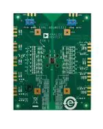
PHOTOGRAPH OF THE EVALUATION BOARD
Figure 1. EVAL-ADuM3151Z Evaluation Board
PLEASE SEE THE LAST PAGE FOR AN IMPORTANT
WARNING AND LEGAL TERMS AND CONDITIONS.
Rev. 0 | Page 1 of 9
�UG-720
EVAL-ADuM3151Z User Guide
TABLE OF CONTENTS
Features .............................................................................................. 1
Power Input ....................................................................................3
Supported SPIsolator Models .......................................................... 1
Data I/O Structures .......................................................................4
General Description ......................................................................... 1
Bypass on the PCB ........................................................................5
Photograph of the Evaluation Board.............................................. 1
High Voltage Capability ...............................................................5
Revision History ............................................................................... 2
Evaluation Board Schematics and Artwork ...................................6
Evaluation Board Circuitry ............................................................. 3
Ordering Information .......................................................................8
PCB Evaluation Goals .................................................................. 3
Bill of Materials ..............................................................................8
Connectors .................................................................................... 3
Related Links ......................................................................................9
REVISION HISTORY
7/14—Revision 0: Initial Version
Rev. 0 | Page 2 of 9
�EVAL-ADuM3151Z User Guide
UG-720
EVALUATION BOARD CIRCUITRY
PCB EVALUATION GOALS
SCOPE PROBE
The EVAL-ADuM3151Z board is intended to achieve the
following goals:
•
•
•
Evaluate the full range of SPIsolator data transfer
functions.
Power each side of the SPIsolator isolator independently.
Allow high differential voltage to be applied between the
two sides of the SPIsolator isolator.
Allow connecting easily to power, other circuit boards and
instrumentation.
SMA CONNECTOR
SCOPE PROBE HEADER
PADS TO
CONNECT
SMA
Although the evaluation board comes with the ADuM3151BRSZ
SPIsolator digital isolator installed, the board is also compatible
with the ADuM3151ARSZ. ADuM3152ARSZ, ADuM3152BRSZ,
ADuM3153ARSZ, and ADuM3153BRSZ.
CONNECTORS
The PCB provides support for three types of interconnections:
•
•
•
SMA edge-mounted connectors.
Through-hole signal ground pairs.
Terminal blocks for power connections.
With these three options, both temporary and permanent
connections to the board can easily be made.
When coaxial connections are desired, SMA connector positions
are available for VDD1 and VDD2 power supplies, as well as all
digital inputs. These SMA connector positions are left
unpopulated so that the user can customize the connectors
for a given application.
Pins that are outputs only may not have access to a coaxial
connection. The native output buffers of the ADuM3151/
ADuM3152/ADuM3253 are not capable of driving a 50 Ω coaxial
terminated cable. Bring out signals leaving the board through the
provided through holes or headers.
Figure 2 shows examples of installed SMA connectors; these
connectors were chosen because they are not only low profile
and provide excellent mechanical connections to the PCB but
also support 50 Ω coaxial cabling. Because most lab equipment is
compatible with BNC connectors, adaptors may be required to
use some on-board connectors.
SHORTING
JUMPER
12437-002
•
Figure 2. Optional Components
Power can be connected through the T1 and T2 terminal blocks or
can be wired directly to the PCB via the PR1 and PR2 throughhole positions or the VDD1 and VDD2 SMA connectors can be
populated to connect the coaxial cable. Each through-hole pair
provides a power and ground with the power on the Pin 1 hole.
The pin spacing of each through-hole connector is 200 mil
between centers. This matches the pin spacing required for
Tektronix active scope probes. If a scope probe connection is
desired, the header shown in Figure 2 can be soldered into the
through-hole positions, and the signal pin can be trimmed to
match the height requirements of a Tektronix active scope probe.
POWER INPUT
Each side of the EVAL-ADuM3151Z SPIsolator isolator requires
an off-board power source. Each power source must be
independent if common-mode voltages are to be applied across
the isolation barrier. Sharing a single supply for both sides of the
part across the isolation barrier does not harm the isolator, and it
is useful for functional testing of the ADuM3151 SPIsolator
isolator when common-mode voltages are not present.
A ground plane and a power plane are present on Layer 2 and
Layer 3 of the PCB on each side of the isolation barrier. Power
connects to the VDD1 and GND1 planes for Side 1 and connects
to the VDD2 and GND2 planes for Side 2.
Rev. 0 | Page 3 of 9
�UG-720
EVAL-ADuM3151Z User Guide
DATA I/O STRUCTURES
Figure 3 shows four 0603 pad layouts between the signal path
and optional connections. Pads with similar functions are
arranged in vertical rows and their function is labeled on the
PCB.
Each data channel has a variety of structures to help configure,
load, and monitor both the input and output. Figure 3 shows one
of the data paths from an external connection to the DUT pin.
Each channel has the same or a subset of these connections
depending on the particular I/O.
•
Starting at the external connection, the signal path is
3.
4.
5.
Pad layout for a PCB board edge-mounted SMA connector.
Two 0805 pads are provided where 100 Ω resistors to
ground can be installed. The combined resistance of 50 Ω
provides a termination for a standard coaxial cable.
A 3-pin 100 mil header is provided, where Pin 1 is
connected to ground through a 10 kΩ resistor, and Pin 3 is
connected to VDD through a 10 kΩ resistor. Temporary
pull-up or pull-down can be implemented with a shorting
jumper between Pin 2 and either Pin 1 or Pin 3.
A 2-pin 100 mil header provides a signal ground pair that
can be used for clip leads or for shorting a channel to
ground temporarily.
There are groupings of three open through holes, consisting
of a signal and two ground connections. These holes can be
used for hardwiring signal wires into the PCB, installing a
header to accept a Tektronix active probe, or installing a
2-pin header to allow adjacent channels to temporarily be
shorted together.
•
•
•
Figure 2 shows many of the optional components installed, as well
as how jumpers can be used to temporarily connect channels.
This figure shows a signal connected to the first channel SMA
and then fanned out to the top three channels and monitored by
an active scope probe.
5 OPEN HOLES FOR SOLDERED WIRES
OR 200mil TEKTRONIC HEADER,
GND/GND/SIGNAL
2 TERMINATION
2 POSITIONS
4 2-PIN HEADER
GND/SIGNAL
3 3-PIN HEADER
FOR 10kΩ LOADS
1 SMA CONNECTOR PADS
NOTES:
1. THE NUMBERED COMPONENTS IN THIS DIAGRAM CORRESPOND TO THE DESCRIPTIONS
IN THE DATA I/O STRUCTURES SECTION.
12437-003
1.
2.
LOAD is a connection to load structures located on the
reverse side of the board. These structures consist of
100 kΩ resistors to power and ground to pull high-Z
outputs to a midrange voltage when not being actively
driven. This is useful during debugging because it allows
easy identification floating outputs. The header and
associated resistors identified in Point 3 are also connected
to the signal path by this pad.
PULL-DOWN is an 0603 pad layout between the signal
path and GND1 or GND2 can be used for installing a
permanent pull-down resistor or load capacitor.
SMA CONNECT is an 0603 pad layout that allows
connection of the data path to the board edge SMA pad
layout and terminations.
PULL-UP is an 0603 pad layout between the signal path
and VDD1 or VDD2 can be used for installing a permanent
pull-up resistor.
Figure 3. Configuration and Monitoring Structures (Showing a Datapath from an External Connection to the DUT Pin)
Rev. 0 | Page 4 of 9
�EVAL-ADuM3151Z User Guide
UG-720
BYPASS ON THE PCB
HIGH VOLTAGE CAPABILITY
Several positions and structures are provided to allow optimum
bypass of the evaluation board. Provision has been made for
optional surface-mount bulk capacitors to be installed near
the power connectors to compensate for long cables to the
power supply. Parallel bypass capacitors are installed near the
ADuM3151BRSZ and consist of a 0.1 µF capacitor for VDD1 on
the top side and bottom side and a 0.1 µF capacitor for each
VDD2 on the top and bottom side of the board. It is best to use
the top side bypass positions if possible.
This PCB is designed in adherence with 3750 V basic insulation
practices. High voltage testing beyond 3750 V is not recommended.
Take appropriate care when using this evaluation board at high
voltages, and do not rely on the PCB for safety functions because it
has not been high potential tested (also known as hipot tested
or dielectric withstanding voltage tested) or certified for safety.
The PCB also implements a distributed capacitive bypass on the
PCB. This consists of power and ground planes closely spaced
on the inner layers of the PCB. This minimizes noise and the
transmission of EMI without using complex design features.
Rev. 0 | Page 5 of 9
�UG-720
EVAL-ADuM3151Z User Guide
EVALUATION BOARD SCHEMATICS AND ARTWORK
SIDE 1 PINS
SIDE 2 PINS
VDD1
VDD2
R13
MCLK_DUT
MCLK_DUT
MO_DUT
MI_DUT
MSSB_DUT
VIA_DUT
VIB_DUT
VOC_DUT
0
R11
1
2
3
P1A
DGND1
DGND1
P1B
DGND1
1
2
SSW-102-01-G-S
VDD1
R14
U1
1 (1) (20)
2 (2) (19)
3 (3) (18)
4 (4) (17)
5 (5) (16)
6 (6) (15)
7 (7) (14)
8 (8) (13)
9 (9) (12)
10 (10) (11)
20
19
18
17
16
15
14
13
12
11
VDD2
GND2
SCLK
SI
SO
SSSB/SS0
VOA/VIA/SS1
VOB/VIB/SS2
VIC/SS3
GND2
VDD2
SCLK_DUT
SCLK_DUT
SI_DUT
SO_DUT
SSSB_DUT
VOA_DUT
VOB_DUT
VIC_DUT
C7
DGND1
DGND1
R17
GEN_SSOP20
P8B
R3
R50
100k
DGND2
100k
ADuM315x
R51
MO_DUT
1
2
SSW-102-01-G-S
VDD2
R52
DGND2
VDD2
10k
1
2
3
MO
P8A
R49
10k
DGND2
R16
1
1
2
3
DGND2
0
MO
2 3 4 5
R48
15PF
DGND2
0
R2
100
0
R1
100
2 3 4 5
VDD1
GND1
MCLK
MO
MI
MSSB
VIA/VOA/SSA0
VIB/VOB/SSA1
VOC/DCLK
GND1
VDD1
R12
MCLK
0
1
0
R47
0
MLCK
PR1
0
1
2
1
2
3
P2A
DGND1
VDD2
DGND1
P2B
DGND1
1
2
SSW-102-01-G-S
DGND1
T1
1
2
KRM2 02
C1T
0.1UF
DGND1
DGND1
VDD1
C1B
0.1UF
DGND1
5 4 3 2
10UF
0.1UF
DGND1
DGND1
0
C8
R54
15PF
DGND2
DGND1
SI_DUT
R59
SI
C1
C2T DNI
R53
VDD1
1
VDD1
0
100
DGND1
1
2
3
0
0
100
JP5
R15
R4
P9A
R19
P9B
R55
R56
100k
DGND2
100k
0
PR2
1
2
MI_DUT
1
2
SSW-102-01-G-S
VDD2
DGND2
C3
DGND2
T2
1
2
KRM2 02
P3B
R21
100k
1
2
SSW-102-01-G-S
VDD1
DGND1
DGND2
R22
R23
10k
DGND1
10k
1
VDD2
C4T
C2B
0.1UF
DGND2
0.1UF
DGND2
C3T
0.1UF
DGND2
DNI
R57
R58
10k
DGND2
10k
VDD2
R60
VDD2
C2
10UF
DGND2
JP6
5 4 3 2
R64
SO
DGND2
1
VDD1
R63
SO
SO_DUT
0
1
2
3
2 3 4 5
JP1
R61
R62
100
100
P10A
P10B
DGND2
DGND2
VDD1
1
2
SSW-102-01-G-S
DGND2
R25
1
R24
MSSB
DGND2
VDD2
0
MSSB
1
2
3
R65
0
R20
100k
DGND1
VDD2
0
P3A
0
1
2
3
0
15PF
DGND1
1
2
3
R18
MSSB_DUT
R66
100
R26
SSSB_DUT
1
2
3
P4A
DGND1
DGND1
C9
P4B
DGND1
1
2
SSW-102-01-G-S
VDD1
P11B
R68
R69
100k
DGND2
100k
1
2
SSW-102-01-G-S
VDD2
DGND2
0
AUX1_S1
VIA_DUT
R28
100
C4
R27
15PF
R71
10k
DGND2
10k
VDD2
1
2
3
P5A
DGND1
JP7
VDD2
P5B
DGND1
R30
R31
100k
100k
1
2
SSW-102-01-G-S
VDD1
DGND1
R72
0
R8
DGND1
R70
1
2
3
R7
100
0
0
DGND1
AUX1_S2
VOA_DUT
R33
R32
1
2
3
0
DGND2
VIB_DUT
100
15PF
R77
R78
100k
DGND2
100k
R79
R80
10k
VDD2
JP8
VDD2
P6B
R38
100k
DGND1
100k
1
2
SSW-102-01-G-S
VDD1
R39
R40
10k
DGND1
10k
R81
0
R37
DGND1
VOB_DUT
AUX2_S2
R83
1
VOB
0
VDD1
R82
1
2
3
1
2
3
P13A
C11
R84
R85
15PF
100
100
0
DGND1
DGND2
DGND2
VDD2
10k
DGND2
1
2
3
P6A
DGND1
DGND1
5 4 3 2
1
2
3
R34
1
2
SSW-102-01-G-S
VDD1
5 4 3 2
DGND2
DGND2
P13B
JP3
DGND2
R86
R87
100k
DGND2
100k
DGND2
VDD2
R42
R88
R89
10k
DGND2
10k
0
VOC_DUT
VDD2
1
2
3
C6
15PF
DGND1
1
2
3
R41
0
P7A
VDD2
JP9
R90
R43
R44
100k
DGND1
100k
1
2
SSW-102-01-G-S
AUX3_S2
R92
VIC_DUT
DGND1
1
VIC
R46
VDD1
1
2
3
P14A
10k
R91
C12
R93
R94
0
0
R45
15PF
100
100
DGND2
P14B
1
2
SSW-102-01-G-S
JP4
DGND2
R95
R96
100k
DGND2
100k
Rev. 0 | Page 6 of 9
DGND2
DGND2
R97
R98
10k
JP10
Figure 4. EVAL-ADuM3151Z Schematic
5 4 3 2
VDD2
10k
DGND2
1
2
3
10k
DGND1
VDD1
0
P7B
1
2
3
100
C5
0
0
R10
R75
100
DGND2
1
2
SSW-102-01-G-S
R36
R9
15PF
R74
100
P12B
R35
VIB
R73
C10
0
1
2
3
P12A
VDD1
AUX2_S1
1
VOA
0
JP2
1
R76
VDD1
10k
10k
DGND1
VDD2
12437-004
VIA
1
2 3 4 5
1
2
3
P11A
DGND1
R29
2 3 4 5
R67
15PF
DGND2
0
R6
0
R5
100
0
0
2 3 4 5
�EVAL-ADuM3151Z User Guide
UG-720
Figure 5. Top Side Layout
Rev. 0 | Page 7 of 9
�UG-720
EVAL-ADuM3151Z User Guide
ORDERING INFORMATION
BILL OF MATERIALS
Table 1. Installed Components
Quantity
1
1
2
2
10
Reference Designator(s)
EVAL-ADuM3151Z
U1
C1, C2
C2T, C3T
JP1 to JP10
14
P1B to P14B
20
R20, R21, R30, R31, R37,
R38, R43, R44, R49, R50,
R55, R56, R68, R69, R77,
R78, R86, R87, R95, R96
R22, R23, R32, R33, R39,
R40, R45, R46, R51, R52,
R57, R58, R70, R71, R79,
R80, R88, R89, R97, R98
T1, T2
20
2
Value
Voltage
Tolerance
10 µF
0.1 µF
Jumper
(3-pin)
Jumper
(2-pin)
100 kΩ
6.3 V
16 V
10%
5%
1/10 W
10 kΩ
Package
1
SSOP20
0805
0603
1 × 3 pin
header
IDC 2×1
IDC 2×1
R0603
1%
0603
5.08 MM
2 × 1 screw
terminal
block
Manufacturer/Part Number
Analog Devices, Inc. 08-038567 Rev A
Analog Devices, Inc. ADuM3151BRSZ
Taiyo Yuden JMK212B7106KG-T
Kemet C0603C104J4RACTU
Harwin M20-9990345
FCI 90726-402HLF
Stackpole RMCF0603FT100K
Panasonic ERJ-3EKF1002V
DIG01 ED2609-ND
Table 2. Optional Components—Not Installed
Quantity
4
16
Reference Designator(s)
C1B, C1T, C2B, C4T
P1A to P14A, PR1, PR2
Value
0.1 µF
Jumper
(2-pin)
Voltage
16 V
Tolerance
5%
10
11
C3 to C12
MO, SO, MLCK, MSSB,
VDD1, VDD2, AUX1_S1,
AUX1_S2, AUX2_S1,
AUX2_S2, AUX3_S2
R1 to R10, R61, R62, R74,
R75, R84, R85, R93, R94
R11 to R19, R24 to R29,
R34 to R36, R41, R42, R47,
R48, R53, R54, R59, R60,
R63 to R67, R72, R73, R76,
R81 to R83, R90 to R92
15 pF
SMA
connector
50 V
5%
100 Ω
1/10 W
0Ω
1/10 W
18
40
1
Package
0603
1 × 2 pin
header
200 mil
0603
CONNPCB coax
SMA end
launch
R0805
Panasonic ERJ-6ENF1000V
1
R0603
Panasonic ERJ-3GEY0R00V
Rev. 0 | Page 8 of 9
Manufacturer/Part Number
Kemet C0603C104J4RACTU
SAMTEC MTSW-202-12-G-S-730 ZZZ
Kemet 15PF 50V 5% 0603 NPO ZZZ
Johnson 142-0701-851
�EVAL-ADuM3151Z User Guide
UG-720
RELATED LINKS
Resource
ADuM3151
ADuM3152
ADuM3153
AN-1109
Description
Product Page, 3.75 kV, 7-Channel SPIsolator Digital Isolators for SPI
Product Page, 3.75 kV, 7-Channel SPIsolator Digital Isolators for SPI
Product Page, 3.75 kV, 7-Channel SPIsolator Digital Isolators for SPI
Application Note, Recommendations for Control of Radiated Emissions with iCoupler Devices
ESD Caution
ESD (electrostatic discharge) sensitive device. Charged devices and circuit boards can discharge without detection. Although this product features patented or proprietary protection
circuitry, damage may occur on devices subjected to high energy ESD. Therefore, proper ESD precautions should be taken to avoid performance degradation or loss of functionality.
Legal Terms and Conditions
By using the evaluation board discussed herein (together with any tools, components documentation or support materials, the “Evaluation Board”), you are agreeing to be bound by the terms and conditions
set forth below (“Agreement”) unless you have purchased the Evaluation Board, in which case the Analog Devices Standard Terms and Conditions of Sale shall govern. Do not use the Evaluation Board until you
have read and agreed to the Agreement. Your use of the Evaluation Board shall signify your acceptance of the Agreement. This Agreement is made by and between you (“Customer”) and Analog Devices, Inc.
(“ADI”), with its principal place of business at One Technology Way, Norwood, MA 02062, USA. Subject to the terms and conditions of the Agreement, ADI hereby grants to Customer a free, limited, personal,
temporary, non-exclusive, non-sublicensable, non-transferable license to use the Evaluation Board FOR EVALUATION PURPOSES ONLY. Customer understands and agrees that the Evaluation Board is provided
for the sole and exclusive purpose referenced above, and agrees not to use the Evaluation Board for any other purpose. Furthermore, the license granted is expressly made subject to the following additional
limitations: Customer shall not (i) rent, lease, display, sell, transfer, assign, sublicense, or distribute the Evaluation Board; and (ii) permit any Third Party to access the Evaluation Board. As used herein, the term
“Third Party” includes any entity other than ADI, Customer, their employees, affiliates and in-house consultants. The Evaluation Board is NOT sold to Customer; all rights not expressly granted herein, including
ownership of the Evaluation Board, are reserved by ADI. CONFIDENTIALITY. This Agreement and the Evaluation Board shall all be considered the confidential and proprietary information of ADI. Customer may
not disclose or transfer any portion of the Evaluation Board to any other party for any reason. Upon discontinuation of use of the Evaluation Board or termination of this Agreement, Customer agrees to
promptly return the Evaluation Board to ADI. ADDITIONAL RESTRICTIONS. Customer may not disassemble, decompile or reverse engineer chips on the Evaluation Board. Customer shall inform ADI of any
occurred damages or any modifications or alterations it makes to the Evaluation Board, including but not limited to soldering or any other activity that affects the material content of the Evaluation Board.
Modifications to the Evaluation Board must comply with applicable law, including but not limited to the RoHS Directive. TERMINATION. ADI may terminate this Agreement at any time upon giving written notice
to Customer. Customer agrees to return to ADI the Evaluation Board at that time. LIMITATION OF LIABILITY. THE EVALUATION BOARD PROVIDED HEREUNDER IS PROVIDED “AS IS” AND ADI MAKES NO
WARRANTIES OR REPRESENTATIONS OF ANY KIND WITH RESPECT TO IT. ADI SPECIFICALLY DISCLAIMS ANY REPRESENTATIONS, ENDORSEMENTS, GUARANTEES, OR WARRANTIES, EXPRESS OR IMPLIED, RELATED
TO THE EVALUATION BOARD INCLUDING, BUT NOT LIMITED TO, THE IMPLIED WARRANTY OF MERCHANTABILITY, TITLE, FITNESS FOR A PARTICULAR PURPOSE OR NONINFRINGEMENT OF INTELLECTUAL
PROPERTY RIGHTS. IN NO EVENT WILL ADI AND ITS LICENSORS BE LIABLE FOR ANY INCIDENTAL, SPECIAL, INDIRECT, OR CONSEQUENTIAL DAMAGES RESULTING FROM CUSTOMER’S POSSESSION OR USE OF
THE EVALUATION BOARD, INCLUDING BUT NOT LIMITED TO LOST PROFITS, DELAY COSTS, LABOR COSTS OR LOSS OF GOODWILL. ADI’S TOTAL LIABILITY FROM ANY AND ALL CAUSES SHALL BE LIMITED TO THE
AMOUNT OF ONE HUNDRED US DOLLARS ($100.00). EXPORT. Customer agrees that it will not directly or indirectly export the Evaluation Board to another country, and that it will comply with all applicable
United States federal laws and regulations relating to exports. GOVERNING LAW. This Agreement shall be governed by and construed in accordance with the substantive laws of the Commonwealth of
Massachusetts (excluding conflict of law rules). Any legal action regarding this Agreement will be heard in the state or federal courts having jurisdiction in Suffolk County, Massachusetts, and Customer hereby
submits to the personal jurisdiction and venue of such courts. The United Nations Convention on Contracts for the International Sale of Goods shall not apply to this Agreement and is expressly disclaimed.
©2014 Analog Devices, Inc. All rights reserved. Trademarks and
registered trademarks are the property of their respective owners.
UG12437-0-7/14(0)
Rev. 0 | Page 9 of 9
�