EVAL-ADuM4160EBZ User Guide
UG-043
One Technology Way • P.O. Box 9106 • Norwood, MA 02062-9106, U.S.A. • Tel: 781.329.4700 • Fax: 781.461.3113 • www.analog.com
iCoupler ADuM4160/ADuM3160 USB Isolator Evaluation Board
INTRODUCTION
EVAL-ADuM4160EBZ EVALUATION BOARD
USB use has displaced older communications standards, such
as RS-232, as the default serial communications port in PC-based
systems. When compared to these other standards, USB has
many enhanced features, such as power for peripherals, automatic
driver installation, and higher data rates. However, when using
USB, it is difficult to provide isolation, which has limited its
acceptance in medical and industrial applications.
This USB evaluation board comes populated with an ADuM4160;
however, because the ADuM4160 and ADuM3160 are electrically
identical and pin compatible, any evaluation done with this board
and component also applies directly to the ADuM3160. If the
user wants to substitute the ADuM3160 on the printed circuit
board (PCB), no other changes are required.
The design goals of this evaluation platform are to
Connect to systems through standard USB Type A and
Type B connectors.
Draw power from the USB host or from an external 5.0 V
or 3.3 V power supply.
Support isolated power for the downstream interface
through an ADuM5000 isoPower® dc-to-dc converter.
Support external downstream power from a 5 V or 3.3 V
power supply.
Provide test points for all power and signal paths.
Support low and full speed communications.
Support enumeration control.
Support external electrostatic discharge (ESD) protection.
Support common-mode chokes in the xD+/xD− lines.
Support ferrite inductors in the VBUSx and GNDx lines.
For full details, see the ADuM4160 and the ADuM3160 data
sheets, which must be used in conjunction with this user guide
when using the EVAL-ADuM4160EBZ evaluation board.
PLEASE SEE THE LAST PAGE FOR AN IMPORTANT
WARNING AND LEGAL TERMS AND CONDITIONS.
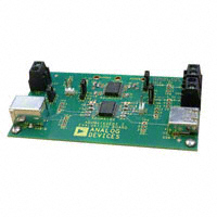
08418-001
Analog Devices, Inc., has introduced the ADuM4160 and
ADuM3160 iCoupler® USB isolators to address the difficult task
of isolating the bus. The EVAL-ADuM4160EBZ USB isolator
evaluation board allows for an easy interface to existing
applications by standard cabling or discrete wiring.
Figure 1.
FEATURES OF THE ADuM4160/ADuM3160
The ADuM4160 and ADuM3160 provide support for full speed
and low speed data communications by interfacing directly with
the USB xD+ and xD− lines. The devices are designed to be
transparent to USB data traffic other than adding about as much
delay as a hub and cable. Features of the isolator include the
following:
Built in voltage regulators that allow the ADuM4160 and
the ADuM3160 to draw power from either 5 V or 3.3 V
sources.
Application of an upstream pull-up resistor is under the
control of the downstream pin, PIN (Pin 12).
Pins on the upstream and downstream sides of the device,
SPU and SPD (Pin 5 and Pin 13, respectively), can set the
operating speed of the isolator.
The upstream side of the isolator includes Pin 1 through Pin 8,
is connected to the left side of the evaluation board, and interfaces through a Type B connector. The downstream facing side
includes Pin 9 through Pin 16, is connected to the right side of
the evaluation board, and interfaces through a Type A connector.
The evaluation board allows configuration of the features of the
ADuM4160/ADuM3160 chip and provides support for a variety
of possible power schemes. The evaluation board also allows
common-mode voltages; however, it is not recommended for
performing safety related testing, such as high voltage withstand
testing. Perform this type of testing on the component level or
on a production board.
Rev. B | Page 1 of 8
�UG-043
EVAL-ADuM4160EBZ User Guide
TABLE OF CONTENTS
Introduction ...................................................................................... 1
Speed Selection ..............................................................................4
EVAL-ADuM4160EBZ Evaluation Board ..................................... 1
Pull-Up Control .............................................................................4
Features of the ADuM4160/ADuM3160 ....................................... 1
Series Resistors...............................................................................4
Revision History ............................................................................... 2
Test Points ......................................................................................4
Power .................................................................................................. 3
Optional Components ..................................................................4
Upstream Side ............................................................................... 3
Evaluation Board Schematic and Artwork.....................................5
Downstream Side.......................................................................... 3
Ordering Information .......................................................................8
Grounding Scheme....................................................................... 3
Bill of Materials ..............................................................................8
REVISION HISTORY
7/2017—Rev. A to Rev. B
Changed from EVAL-ADuM4160EBZ/ADuM3160EBZ User
Guide to EVAL-ADuM4160EBZ User Guide ............ Throughout
Changes to Features of the ADuM4160/ADuM3160 Section .... 1
Changed Evaluation Board Section to EVAL-ADuM4160EBZ
Evaluation Board Section ................................................................ 1
Changes to Upstream Side Section and Downstream Side
Section ................................................................................................ 3
Changes to Table 4, Series Resistors Section, Test Points Section,
and Optional Components Section ................................................ 4
Changes to Figure 3 .......................................................................... 6
Added Figure 4 .................................................................................. 6
Added Figure 5 and Figure 6 ........................................................... 7
Added Ordering Information Section, Bill of Materials Section,
and Table 5 ......................................................................................... 8
9/2010—Rev. 0 to Rev. A
Added ADuM3160 ........................................................ Throughout
Changes to Introduction ..................................................................1
2/2010—Revision 0: Initial Version
Rev. B | Page 2 of 8
�EVAL-ADuM4160EBZ User Guide
UG-043
POWER
UPSTREAM SIDE
The USB standard requires that the upstream facing port of a
peripheral device derive power for its pull-up from the 5 V present
on the cable. Power can also be used to power functions in the
peripheral at up to 500 mA.
The ADuM4160 and ADuM3160 contain an internal voltage
regulator that can derive the 3.3 V from VBUSx for use in the data
transmission and pull-up power. The user can bypass this regulator
if 3.3 V is provided from an external supply. The evaluation
board can source its power either from the cable at 5 V or from
an external supply connected to J5 terminal block, EXT. Jumper
JP1 selects between the two sources. When external power is
chosen, the ADuM3160 and ADuM4160 can be configured to
accept either 3.3 V or 5 V from that source. If 3.3 V is supplied,
the internal regulator must be disabled by shorting Pin 1 and
Pin 3 together. Shorting Pin 1 and Pin 3 is accomplished by
placing a shunt across JP3, 3.3EXT. This jumper must be open
when the USB bus is the source of power.
Table 1. Upstream Power Jumper Settings
Power Source
USB Bus
EXT 5.0 V
EXT 3.3 V
Jumper Settings
IN SELU (JP1)
3.3EXT (JP3)
USB (2 and 3)
Open
EXT (1 and 2)
Open
EXT (1 and 2)
Short
The ADuM5000 can provide a maximum 500 mW of power to
the downstream side. Applications that require more power at
the downstream port must use the external 5 V power supply
option. The ADuM5000 is provided for the convenience of the
user, and its use in final applications must be reviewed based on
its data sheet precautions for power consumption and
electromagnetic interference (EMI) mitigation.
Configuration of the downstream power is accomplished by
installing or uninstalling the ADuM5000 converter, applying
power to J3 or J4, and setting the appropriate jumper.
As with the upstream side of the ADuM4160 or the ADuM3160,
there is an internal regulator that derives the 3.3 V supply for the
xD+ and the xD− signal lines from a 5 V source applied to
VBUS2. In addition, if VBUS2 and VDD2 are connected together to a
3.3 V source, the regulator is bypassed, and the voltage is used
directly by the chip. The IN SELD (JP3) jumper selects between
deriving power from a 5 V source and a 3.3 V source. The 5 V
source can either be an external voltage applied to J3 or an
ADuM5000. The only 3.3 V source is the J4 terminal block. If
external power is used, the ADuM5000 must not be installed on
the board.
Table 2. Downstream Power Jumper Settings
DOWNSTREAM SIDE
The USB standard does not allow any power to be sourced
from a peripheral port. Power to run the downstream side of
the ADuM4160 or ADuM3160 cannot come from the cable
connection as it did on the upstream facing side. If the isolator
is built into a peripheral device, it can receive power directly
from the power supply of the peripheral. If the isolator is not
built into the peripheral that it is protecting, power must be
provided from an external source or derived from the upstream
bus power through a dc-to-dc converter. All of these possible
power configurations are addressed in the evaluation board.
Power for the downstream port can be provided from an
external 5 V power supply through Terminal Block J3 or from
the upstream USB power bus through an ADuM5000 isoPower
isolated dc-to-dc converter. The ADuM5000 is shipped loose
with the evaluation board and must be soldered to the evaluation
board in the U2 position if isolated power is provided by the
upstream USB power bus. Only one method of powering the
downstream port can be used.
Power Source
USB Bus
5 V (J3)
3.3 V (J4)
Jumper Settings/Components
IN SELD (JP3)
ADuM5000
5 V/USB
Installed
5 V/USB
Not installed
3.3 V
Not installed
GROUNDING SCHEME
The evaluation board consists of two separate ground and
power systems. In addition, there is a floating capacitive
structure on the bottom layer of the PCB that provides EMI
mitigation for the ADuM5000 dc-to-dc converter. This structure
consists of a floating plane on each side of the isolation
boundary. To allow evaluation of different EMI mitigation
schemes, the planes can be, for example,
•
•
•
Rev. B | Page 3 of 8
Left floating, which has a minimal effect on EMI.
Connected by adding a strip of copper tape and soldering it
to the exposed pads.
Connected by safety capacitors installed in through-hole
positions, C14 and C19.
�UG-043
EVAL-ADuM4160EBZ User Guide
In addition, the ground and power planes can be capacitively
linked via C15 to C18 at the option of the user. This linking can
provide plane-to-plane noise bypassing through several paths to
reduce radiated emissions from the ADuM5000 power supply.
Two large screw holes along the top edge of the PCB provide
connection to the upstream ground plane and the downstream
ground plane. These holes allow grounding of the PCB to the
system in multiple configurations. The floating planes are
designed with 0.4 mm of setback to all vias and other board
planes. If the floating structures are employed for noise reduction,
the PCB must not be used for high voltage testing. When this
type of structure is required in the final design, build it on an
inner layer of the PCB to avoid creepage and clearance issues.
SPEED SELECTION
The ADuM4160 and ADuM3160 work at a fixed USB transmission speed, either low speed or full speed. The SPU pin and
the SPD pin on the upstream and downstream sides of the device
set the speed and must be set by jumpers on the evaluation
board. For proper operation, set both speed jumpers to the
same speed setting.
Table 3. Speed Selection Jumpers
SPU (JP4)
Short SPU Full
Short SPU Low
SPD (JP5)
Short SPD full
Short SPD low
Table 4. PIN Pull-Up Control
PIN (JP6)
Short
Open
Upstream Pull-Up State
Disconnected
Connected
SERIES RESISTORS
The two USB speeds supported by the ADuM4160 and
ADuM3160 require different series resistance values at the
transceiver terminals.
For full speed operation, the R1, R2, R3, and R4 resistors must
be populated with 24 Ω, 1% resistors. These 24 Ω resistors are
installed in the base configuration of the evaluation board and,
if the evaluation board is operating at full speed, no changes are
required.
When the ADuM4160 operates at low speeds, it is recommended to modify the evaluation board from the as received
configuration. For low speed operation, replace the R1, R2, R3,
and R4 resistors with 0 Ω, 0805 sized, SMT shunts. If impedance is
not critical, the 24 Ω resistors do not significantly affect the low
speed performance, and they can be left in place for both speed
modes.
TEST POINTS
Speed
Full (12 Mbps)
Low (1.5 Mbps)
PULL-UP CONTROL
The PIN pin allows control of enumeration and disconnect by the
peripheral. When PIN is logic high, the pull-up on the upstream
side of the ADuM4160 or the ADuM3160 is applied to the data
line appropriate for the USB speed mode, which allows enumeration and data transmission. When PIN is logic low, the
upstream pull-up is disconnected, making the upstream port
behave as though the port were not present.
This function allows the peripheral to delay communication
with the host by delaying application of the upstream pull-up
resistor until it is ready to enumerate on the bus. If this functionality is not required, tie PIN to VDD2, and when power is
applied to both the downstream power supplies, the pull-up is
applied to the upstream side.
Jumper JP6 provides control of PIN. A 10 kΩ resistor pulls the
PIN input high. When a shunt is placed across JP6, it is pulled
low, which provides a default state of high to PIN, allowing
immediate enumeration.
Positions for eight test points are included on the evaluation
board. No headers are provided in the default configuration.
Mounting holes for a ground signal pair are provided. The holes
fit a standard square pin spaced at 100 mil or 200 mil on center.
This configuration was chosen to match the dimensions of the
Tektronix® high frequency active probes or standard headers. To
obtain an appropriate scope header use a 3-pin SIP (2.54 mm
spacing) wire wrap header and remove the center pin. The
signal pin can be trimmed to match the spacing of the probe. If
another type of connection is required, insert wires into the
holes provided for these connections.
OPTIONAL COMPONENTS
Options for installing common-mode chokes and external ESD
protection on the DD+/DD− and UD+/UD− data lines are available on the EVAL-ADUM4160EBZ evaluation board. Positions
for 1206-sized Wurth WE-CNSW chokes are provided at
Position FL1 and Position FL2. Positions for ESD diode packs
(NUP2202 from ON Semiconductor®) are provided at Position D1
and Position D2. In addition, pads for surface-mount ferrite
inductors are provided at Position R6 to Position R10. These
positions are included on the PCB as a convenience to the end
user and are not necessary for operation. To make use of
common-mode chokes, remove the R11, R12, R13, and R14
shunts.
Rev. B | Page 4 of 8
�1
2
3
4
USB-B-S-F-B-TH-R
J2
25.161.0253
1
2
AGND_A
R7
R8
TBD0805
DNI
TBD0805
DNI
DNI
R6
1
2
3
AGND_A
TP3
DNI
1
2
3
TP2 DNI
1
22-03-2031
2
3
TP1 DNI
22-03-2031 1
2
3
22-03-2031
JP1
TBD0805
DNI
1
JP3
4
1
+5V
NC
VP
5
JP4
NUP2202W1T2G
IO2
6
DNI
D1
0
R12
1
2
3
DNI
FL1
1
2
260OHM AT 100MEGHZ
2
3
0
R11
69157-102HLF
AGND_A
VN
IO1
AGND_A
22-03-2031
+5V
2
22-03-2031
1
2
3
22-03-2031
DNI TP4
+5V
DNI
C1
AGND_A
TBD0805
DNI
TBD0805
DNI
R2
R1
0.1UF
DNI
C15
1
2
3
4
5
6
7
8
1
C18
TBD_SPACER_400
DNI
C19
TBD_SPACER_500
DNI
AGND_A
STHGND
DNI
C17
TBD_SPACER_500
AGND_A
STHGND1
AGND_B
VISO
AGND_B
AGNDB
K24A
ADUM4160BRWZ
R1-R4 TBD 0805
AGNDA
K24A
+5V
1
U1
C3
0.1UF
DNI
16
VBUS1
VBUS2
15
GND1
GND2
14
VDD1
VDD2
13
PDEN
SPD
12
SPU
PIN
11
UD_NEG DD_NEG
10
UD_POS DD_POS
9
GND1
GND2
AGND_A
VDD
C2
0.1UF
VISO
STHGND1
TBD_SPACER_500
DNI
C16
TBD_SPACER_500
AGND_A
ADUM5000ARWZ
ADUM5000
C7
U2
0.1UF
16
1
VDD1
VISO
15
2
GND1 GNDISO
14
3
NC
NC
13
4
RCIN
VSEL
12
5
RCOUT
NC
11
6
RCSEL
NC
10
7
VDD1
VISO
9
8
GND1 GNDISO
FOR 24 OHM 1% USE 0603
FOR 0 OHM USE 0805
+5V
C6
0.1UF
C5
10UF
+5V
TBD0805
C12 +5V
AGND_A
AGND_A
DNI
C14
10K
R5
C4
TBD0805
DNI
AGND_B
1
NC
5
VP
VISO
3
2
4
1
0
R13
AGND_B
VISO
AGND_B
DNI
FL2
AGND_B
6
0
NUP2202W1T2G
IO2
D2
DNI
R14
260OHM AT 100MEGHZ
C11
0.1UF
C9
10UF
VN
IO1
R4
TBD0805
DNI
R3
TBD0805
DNI
VISO
C10
0.1UF
AGND_B
VISO
C8
0.1UF
22-03-2031
JP2
1
2
3
1
2
AGND_B
25.161.0253
1
2
DNI J4
TP6
22-03-2031
DNI
1
2
3
22-03-2031
JP5
1
2
3
DNI
TP5
1
2
22-03-2031
3
AGND_B
69157-102HLF
JP6
TP7
DNI
22-03-2031
1
2
3
DNI TP8
1
22-03-2031
2
3
AGND_B
C13
10UF
R10
J5
4
3
Rev. B | Page 5 of 8
2
Figure 2. EVAL-ADUM4160EBZ Evaluation Board Schematic
4
3
R9
TBD0805
DNI
TBD_SPACER_400
TBD0805
DNI
AGND_B
G1
G2
1
2
3
4
25.161.0253
J3
87520-0010BLF_ALT
GND
PINS
J1
AGND_B
1
2
08418-002
STHGND
EVAL-ADuM4160EBZ User Guide
UG-043
EVALUATION BOARD SCHEMATIC AND ARTWORK
�EVAL-ADuM4160EBZ User Guide
08418-003
UG-043
08418-004
Figure 3. EVAL-ADUM4160EBZ Evaluation Board Layer 1 and Silkscreen
Figure 4. EVAL-ADUM4160EBZ Evaluation Board Layer 2
Rev. B | Page 6 of 8
�UG-043
08418-005
EVAL-ADuM4160EBZ User Guide
08418-006
Figure 5. EVAL-ADUM4160EBZ Evaluation Board Layer 3
Figure 6. EVAL-ADUM4160EBZ Evaluation Board Layer 4 and Silkscreen
Rev. B | Page 7 of 8
�UG-043
EVAL-ADuM4160EBZ User Guide
ORDERING INFORMATION
BILL OF MATERIALS
Table 5.
Qty
1
1
7
3
1
1
1
4
2
4
1
5
9
2
6
2
Reference Designator
U1
U2
C2, C6, C7, C8, C10, C11, C12
C5, C9, C13
J1
J2
J3
JP1, JP2, JP4, JP5
JP3, JP6
R11, R12, R13, R14
R5
Not applicable
R1, R2, R3, R4, R6, R7, R8, R9, R10
C1, C3, C4
C14, C15, C16, C17, C18, C19
D1, D2
2
2
8
FL1, FL2
J4, J5
TP1, TP2, TP3, TP4, TP5, TP6, TP7, TP8
Description
Device under test (DUT)
DUT (shipped with evaluation board; not installed)
X7R, 0805, capacitors
X5R, 0805, capacitors
USB, Type A, PCB connector
USB, Type B, PCB connector
2-position screw terminal
100 mil (2.54 mm) 3-position headers
100 mil (2.54 mm) 2-position headers
0805, 0 Ω, resistors
0805, 10 kΩ, resistor
100 mil (2.54 mm) jumpers
0805, resistors, not installed
0805, capacitors, not installed
Leaded capacitor position, not installed
Transient voltage suppressor (TVS) arrays, not
installed
SMD, common-mode chokes, not installed
2-position screw terminals, not installed
100 mil, 3-position headers, not installed
Manufacturer/Part Number
Analog Devices/ADuM4160BRWZ
Analog Devices/ADuM5000ARWZ
Murata/GRM21BR71H104KA01L
Murata/GRM21BR61C106KE15L
FCI/87520-0010BLF_ALT
SAMTEC/USB-B-S-F-B-TH-R
Wieland/25.161.0253
Molex/22-03-2031
Amphenol FCI/69157-102HLF
Panasonic/ERJ-6GEY0R00V
Panasonic/ERJ-6ENF1002V
FCI/68786-302LF
Not applicable
Not applicable
Not applicable
ON Semiconductor/NUP2202W1T2G
Wurth Elektronik/744232261
Wieland/25.161.0253
Molex/22-03-2031
ESD Caution
ESD (electrostatic discharge) sensitive device. Charged devices and circuit boards can discharge without detection. Although this product features patented or proprietary protection
circuitry, damage may occur on devices subjected to high energy ESD. Therefore, proper ESD precautions should be taken to avoid performance degradation or loss of functionality.
Legal Terms and Conditions
By using the evaluation board discussed herein (together with any tools, components documentation or support materials, the “Evaluation Board”), you are agreeing to be bound by the terms and conditions
set forth below (“Agreement”) unless you have purchased the Evaluation Board, in which case the Analog Devices Standard Terms and Conditions of Sale shall govern. Do not use the Evaluation Board until you
have read and agreed to the Agreement. Your use of the Evaluation Board shall signify your acceptance of the Agreement. This Agreement is made by and between you (“Customer”) and Analog Devices, Inc.
(“ADI”), with its principal place of business at One Technology Way, Norwood, MA 02062, USA. Subject to the terms and conditions of the Agreement, ADI hereby grants to Customer a free, limited, personal,
temporary, non-exclusive, non-sublicensable, non-transferable license to use the Evaluation Board FOR EVALUATION PURPOSES ONLY. Customer understands and agrees that the Evaluation Board is provided
for the sole and exclusive purpose referenced above, and agrees not to use the Evaluation Board for any other purpose. Furthermore, the license granted is expressly made subject to the following additional
limitations: Customer shall not (i) rent, lease, display, sell, transfer, assign, sublicense, or distribute the Evaluation Board; and (ii) permit any Third Party to access the Evaluation Board. As used herein, the term
“Third Party” includes any entity other than ADI, Customer, their employees, affiliates and in-house consultants. The Evaluation Board is NOT sold to Customer; all rights not expressly granted herein, including
ownership of the Evaluation Board, are reserved by ADI. CONFIDENTIALITY. This Agreement and the Evaluation Board shall all be considered the confidential and proprietary information of ADI. Customer may
not disclose or transfer any portion of the Evaluation Board to any other party for any reason. Upon discontinuation of use of the Evaluation Board or termination of this Agreement, Customer agrees to
promptly return the Evaluation Board to ADI. ADDITIONAL RESTRICTIONS. Customer may not disassemble, decompile or reverse engineer chips on the Evaluation Board. Customer shall inform ADI of any
occurred damages or any modifications or alterations it makes to the Evaluation Board, including but not limited to soldering or any other activity that affects the material content of the Evaluation Board.
Modifications to the Evaluation Board must comply with applicable law, including but not limited to the RoHS Directive. TERMINATION. ADI may terminate this Agreement at any time upon giving written notice
to Customer. Customer agrees to return to ADI the Evaluation Board at that time. LIMITATION OF LIABILITY. THE EVALUATION BOARD PROVIDED HEREUNDER IS PROVIDED “AS IS” AND ADI MAKES NO
WARRANTIES OR REPRESENTATIONS OF ANY KIND WITH RESPECT TO IT. ADI SPECIFICALLY DISCLAIMS ANY REPRESENTATIONS, ENDORSEMENTS, GUARANTEES, OR WARRANTIES, EXPRESS OR IMPLIED, RELATED
TO THE EVALUATION BOARD INCLUDING, BUT NOT LIMITED TO, THE IMPLIED WARRANTY OF MERCHANTABILITY, TITLE, FITNESS FOR A PARTICULAR PURPOSE OR NONINFRINGEMENT OF INTELLECTUAL
PROPERTY RIGHTS. IN NO EVENT WILL ADI AND ITS LICENSORS BE LIABLE FOR ANY INCIDENTAL, SPECIAL, INDIRECT, OR CONSEQUENTIAL DAMAGES RESULTING FROM CUSTOMER’S POSSESSION OR USE OF
THE EVALUATION BOARD, INCLUDING BUT NOT LIMITED TO LOST PROFITS, DELAY COSTS, LABOR COSTS OR LOSS OF GOODWILL. ADI’S TOTAL LIABILITY FROM ANY AND ALL CAUSES SHALL BE LIMITED TO THE
AMOUNT OF ONE HUNDRED US DOLLARS ($100.00). EXPORT. Customer agrees that it will not directly or indirectly export the Evaluation Board to another country, and that it will comply with all applicable
United States federal laws and regulations relating to exports. GOVERNING LAW. This Agreement shall be governed by and construed in accordance with the substantive laws of the Commonwealth of
Massachusetts (excluding conflict of law rules). Any legal action regarding this Agreement will be heard in the state or federal courts having jurisdiction in Suffolk County, Massachusetts, and Customer hereby
submits to the personal jurisdiction and venue of such courts. The United Nations Convention on Contracts for the International Sale of Goods shall not apply to this Agreement and is expressly disclaimed.
©2010–2017 Analog Devices, Inc. All rights reserved. Trademarks and
registered trademarks are the property of their respective owners.
UG08418-0-7/17(B)
Rev. B | Page 8 of 8
�