EVAL-ADuMQSEBZ User Guide
UG-042
One Technology Way • P.O. Box 9106 • Norwood, MA 02062-9106, U.S.A. • Tel: 781.329.4700 • Fax: 781.461.3113 • www.analog.com
Evaluating the 16-Lead SOIC and the 16-Lead QSOP Digital Isolators
FEATURES
SUPPORTED iCOUPLER MODELS
Convenient connections for power through screw
terminal blocks
Add-on BNC connector for 50 Ω signal sources
On-board signal routing
Support for signal wrap back
Simple signal paths to reduce transmission line effects
Pull-up and pull-down provided for control lines
Support for isoPower
Project area that supports surface-mount and through-hole
devices
ADuM130x
ADuM131x
ADuM140x
ADuM141x
ADuM1510
ADuM240x
ADuM330x
ADuM340x
ADuM344x
ADuM5000
ADuM520x
ADuM540x
ADuM6000
ADuM620x
ADuM640x
ADuM744x
ADuM7510
GENERAL DESCRIPTION
The EVAL-ADuMQSEBZ can be used with most iCoupler®
isolation products in the 16-lead, wide-body SOIC and QSOP
packages. The evaluation board supports the common pad
positions for power, ground, and input/output pins found in
nearly all of the iCoupler products and is a configurable board
that can be adapted to many iCoupler products.
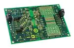
08414-001
EVALUATION BOARD
Figure 1.
PLEASE SEE THE LAST PAGE FOR AN IMPORTANT
WARNING AND LEGAL TERMS AND CONDITIONS.
Rev. C | Page 1 of 8
�UG-042
EVAL-ADuMQSEBZ User Guide
TABLE OF CONTENTS
Features .............................................................................................. 1
Terminals ........................................................................................3
General Description ......................................................................... 1
Data Input/Output Connections .................................................5
Supported iCoupler Models ............................................................ 1
Design Area ....................................................................................5
Evaluation Board .............................................................................. 1
Evaluation Board Schematic and Layout .......................................6
Revision History ............................................................................... 2
Ordering Information .......................................................................8
Evaluation Board Hardware ............................................................ 3
Bill of Materials ..............................................................................8
Pad Layout for the Device Under Test (DUT) .......................... 3
REVISION HISTORY
11/2016—Rev. B to Rev. C
Changes to Supported iCoupler Models Section ......................... 1
10/2015—Rev. A to Rev. B
Changes to Supported iCoupler Models Section ......................... 1
12/2010—Rev. 0 to Rev. A
Changes to Supported iCoupler Models Section ......................... 1
1/2010—Revision 0: Initial Version
Rev. C | Page 2 of 8
�EVAL-ADuMQSEBZ User Guide
UG-042
EVALUATION BOARD HARDWARE
PAD LAYOUT FOR THE DEVICE UNDER TEST (DUT)
08414-003
08414-002
The evaluation board has a pad layout in U2A that accommodates
16-lead, wide-body SOIC devices, as well as QSOP miniature
packages, as shown in Figure 2. Power and ground connections
connect to capacitor pads for Side 1 and Side 2.
(but not populated) to connect the ADuM5000 in master or slave
mode, as well as to set the output voltage. See the ADuM5000
data sheet for descriptions of the pin functions.
Figure 2. DUT Pad Layout Component U2A
Three low inductance, surface-mount bypass capacitors are
provided for each side. A 100 nF capacitor is installed on each
side in Capacitor C2 and Capacitor C3. Additional bypass
capacitors are required for QSOP packages and are below the
QSOP pads and within the pad layout of the SOIC package.
However, they cannot be installed if the SOIC is in use.
In addition, there are 10 µF ceramic, X7R capacitors, C1 on Side 1
and C4 on Side 2, that provide high frequency bypassing and
ripple reduction. For further ripple reduction in isoPower®
devices like the ADuM540x, tantalum capacitors are added to
C10 as a 68 µF value on Side 1 and to C5 as a 22 µF value on
Side 2. These large value ceramic and tantalum bypass capacitors
are not necessary for non-isoPower devices.
Many of the iCoupler devices have configuration pins that allow
outputs to be disabled or default levels to be set. These pins are
usually located at Pin 7 and Pin 10 in the wide body package. Pullup 0 Ω resistors on SM Pad R4 and SM Pad R17 pull these pins
high. These pull-up resistors can be removed, and pull-down
resistors can be installed on R5 and R18.
In addition to the U2A DUT space, an additional pad layout is
provided at U1, specifically to accommodate an ADuM5000
isoPower device, as shown in Figure 3, which is a power supply
only device that can provide secondary power for any iCoupler
in standalone mode or a slave to boost power to the ADuM520x
or ADuM540x devices. The surface-mount resistor pads that
control these functions are not populated.
An ADuM5000 is not installed at Position U1; it is left to the
user to obtain and install this device, if required. As shown in
Figure 3, the power and ground connections for this device are
different from the rest of the iCoupler components. The C6 to
C9 pad positions for bypass capacitors are provided but not
populated (0.1 µF, X7R, ceramic capacitors are recommended).
Pull-up, pull-down, and connecting resistor pads are provided
Figure 3. ADuM5000 Pad Layout Component U1
Grounding Scheme
The evaluation board consists of two separate ground and
power systems. Each side of the DUT can operate from an
independent power and ground reference, which allows
simulation of conditions similar to the target application. The
evaluation board provides for board creepage and clearance
typical of most 2.5 kV circuit boards. It is not recommended for
use above 2.5 kV rms transient voltages or for isolation voltage
testing above 2500 V rms.
Electromagnetic Interference (EMI) and Electromagnetic
Compatibility (EMC) Measurements
The signal path was made as simple as possible while still
providing flexibility. The evaluation board is not intended for
detailed characterization of system noise, EMI, or EMC. It may
be useful for initial bench work in these areas, but Analog Devices,
Inc., does not guarantee that the evaluation board results will be
indicative of the final system performance in these areas. The
evaluation board includes some of the structures discussed in
the AN-0971 Application Note for radiated EMI mitigation.
TERMINALS
Side 1 Power Supply Inputs
Power is supplied to the evaluation board via a set of terminal
block connectors, IO_1C, as shown in Figure 4. Power is connected
to the Pin 1 top terminal, and ground is connected to the Pin 2
top terminal. Provisions for adding in-line inductors for noise
isolation were made with the inclusion of Z1 and Z2, which are
1206 size, surface-mount components. These positions are
populated with 0 Ω resistors to connect power to the evaluation
board. If ferrite inductors are required for noise control, remove
these components and replaced them with appropriate inductors.
Rev. C | Page 3 of 8
�EVAL-ADuMQSEBZ User Guide
08414-005
08414-004
UG-042
Figure 4. Side 1 Terminal Block Connector
Figure 5. Side 2 Terminal Block Connector
The power and ground from the screw terminal block (if
installed) are connected to the Side 1 power and ground pads
of the DUT and provide power and ground to pull-up and pulldown resistors and terminations.
Power is connected to the terminal block connector (if installed),
IO_1D, as shown in Figure 5. Power is connected to IO_1D
Pin 1 at the top, and ground is connected to Pin 2. Provisions
for adding in-line inductors for noise isolation or for isolating
the jacks from the on-board power connections were made with
the inclusion of Z6 and Z7. These positions are populated with
0 Ω resistors to connect power from the ADuM540x to the
IO_1D terminal block.
The ADuM640x devices differ from the rest of the isoPower
devices in that they have an additional power supply input on
Pin 7 that replaces the RCOUT pin present on the ADuM5401,
ADuM5402, ADuM5403, and ADuM5404. Bypass and connect
this pin to VDD1 for proper operation of the ADuM640x. It is
recommended that a 0.1 µF capacitor be installed at R5 and a
0 W resistor at R4. The ADuM640x devices are not compatible
with power sharing; therefore, do not install an ADuM5000 at U1
when using the ADuM640x.
Side 2 Power Supply Connections
The Side 2 connections are different from those on Side 1. With
standard iCoupler devices, these connections are power supply
inputs for Side 2. However, with isoPower devices such as the
ADuM540x, these same connections can be power outputs for
off-board circuits. In addition, they can be configured as an
independent power supply for the project area.
When standard iCoupler isolators are installed, populate the Z6
and Z7 pads with 0 Ω resistors to connect the power jacks to the
power pins of the DUT. Replace these resistors with inductors if
noise isolation is required.
When isoPower devices are installed on the evaluation board,
the power configuration required can vary greatly, depending
on the demands of the application. With 0 Ω resistors or
inductors installed at Z6 and Z7, the power jacks can provide
power from the isoPower device to an external device.
Rev. C | Page 4 of 8
�EVAL-ADuMQSEBZ User Guide
UG-042
DATA INPUT/OUTPUT CONNECTIONS
DESIGN AREA
Side 1 Data Input/Output
The design area of the evaluation board allows breadboarding
of application components such as RS-485 and controller area
network (CAN) transceiver, analog-to-digital converter (ADC),
or digital-to-analog converter (DAC) components with direct
interconnects. The design area, as shown in Figure 6, accepts
most surface-mount narrow- and wide-body components with
50 mil and 100 mil pitch, as well as narrow- and wide-body
300 mil DIP through-hole devices. These surface-mount discrete
components and jumper wires can complete a wide variety of
circuits.
Signals can be provided to the evaluation board and routed to
the required input pins through the IO_1C terminal block
connector, as shown in Figure 4. Four channel inputs/outputs can
be connected from IO_1C Pin 3 through IO_1C Pin 6 to the
respective A, B, C, and D channels of the ADuM540x.
Signals from the IO_1C terminal block connector channels can
also be routed to some of the other data lines through the JP1A
and JP1B jumper blocks (these jumper blocks correspond to
BNC Channel A and Channel B, if you populate them). Each
jumper block allows a channel signal from the IO_1C terminal
block to be connected to additional data input lines by configuring
the jumpers. The jumper blocks can also be used to wrap
signals from an iCoupler output back to an input by using the
JP1A or JP1B block to cross-connect inputs and outputs.
A common way to provide signals is with a function generator
through 50 Ω coax cables. The evaluation board has a layout
position at IO_1A and IO_1B for adding two BNC connectors,
but these are not provided with the evaluation board. The Tyco
AMP 227699-2 coax cables can be purchased to populate these
BNC connectors. In addition, to have 50 Ω terminations on the
evaluation board for the added BNC connectors, add a 50 Ω
through-hole resistor at the R1 and R2 positions. It is possible to
route data outputs to this connector as well; however, it is not
recommended because proper termination is not possible for
logic level signals, and improper termination can cause severe
ringing on the output lines.
The design area has convenient connection points to the
primary data path, CHA to CHD, of the iCoupler, as well as
power connections for VISO and GNDISO. To allow signals from
the design area to be routed to the IO_1D terminal block,
remove the 0 Ω resistors for R23 through R26. Note that no
ground plane is provided in the design area.
The Side 1 input/output structure also includes pull-up/pulldown/load positions, R7 through R14. Discrete through-hole
resistors and capacitors can be installed at these positions to
simulate most loading conditions or to provide pull-ups for
open collector outputs.
Side 2 Data I/O
VISO
Z6
GNDISO
Z7
DESIGN AREA
CHA
CHA
CHB
CHB
CHC
CHC
CHD
In addition to the off-board input/output connections, each
data channel is provided with through-hole connections to the
design area.
Rev. C | Page 5 of 8
IO_1D
1
CHD
R23
R24
R25
R26
8
VISO
Figure 6. Design Area
08414-006
Signals can be provided to the evaluation board and routed to
the required input pins through the IO_1D terminal block
connector, as shown in Figure 5. It consists of terminal block
connections that operate like the Side 1 structures. The terminal
block connections can also be used to wrap signals from an
iCoupler output back to an input.
�Rev. C | Page 6 of 8
999394
1
2
3
4
5
6
IO_1C
Figure 7. Schematic of ADuM540x Evaluation Board
AGND
TSW-104-08-T-D
1
2
3
4
5
6
7
8
JP1A
DP1-1
DP2-1
DP3-1
DP4-1
1
TP_D
1
TP_A
AMP227699-2
1
TP_B
R1
1
TP_C
R9
IO_1A
R8
AGND
5 4 3 2
1
R7
VDD1
R11
R10
R12
1
2
3
4
5
6
7
8
JP1B
R14
AGND
1
1
AGND
GND2
TSW-104-08-T-D
AGND
R13
TBD1206
Z2
TBD1206
Z1
VDD1
1
AGND
GND3
AMP227699-2
R2
R21
TBD0805
AGND
GND1
VDD1
1
R3
IO_1B
AGND
5 4 3 2
1
TBD0805
AGND
R5
TBD1206
R4
TBD1206
VDD1
N
P
TBD0805
C7
TBD0805
C6
VDD1
AGND
C10
68UF
AGND
1
2
3
P1
C1
.1UF
C2
.1UF
AGND
C11
0.1UF
AGND
VDD1
1
2
3
4
5
6
7
8
GEN_SO16WB
1
2
3
4
5
6
7
8
16
15
14
13
12
11
10
9
16
15
14
13
12
11
10
9
U2A
16
15
14
13
12
11
10
9
U2
R22
TBD0805
GEN_QSOP16
R6
TBD0805
GEN_SO16WB
1
2
3
4
5
6
7
8
U1
APLANE
C12
0.1UF
C8
.1UF
C9
.1UF
C4
.1UF
APLANE
R18
TBD1206
R17
TBD1206
V_ISO
C3
.1UF
R16
TBD1206
R15
TBD1206
1
2
3
APLANE
V_ISO
C5
22UF
P2
V_ISO
1
2
3
P3
N
P
1
1
R20
TBD1206
R19
TBD1206
APLANE
R24
1
TBD1206
APLANE
V_ISO
TBD1206
R23
GND_ISO1
V_ISO
Z6
TBD1206
R25
GND_ISO2
TBD1206
Z7
TBD1206
1
1
TPB
1
TPC
1
TPD
TBD1206
R26
GND_ISO3
1
TPA
999394
1
2
3
4
5
6
IO_1D
UG-042
EVAL-ADuMQSEBZ User Guide
EVALUATION BOARD SCHEMATIC AND LAYOUT
08414-007
�UG-042
08414-008
EVAL-ADuMQSEBZ User Guide
Figure 8. Evaluation Board Layout
Rev. C | Page 7 of 8
�UG-042
EVAL-ADuMQSEBZ User Guide
ORDERING INFORMATION
BILL OF MATERIALS
Table 1.
Quantity
2
0
0
1
1
2
2
0
0
2
17
2
0
6
4
0
0
Reference Designator
IO_1C, IO_1D
U1
U2
C10
C5
C1, C4
C2, C3
C6 to C9, C11, C12
IO_1A, IO_1B
JP1A, JP1B
TP_A, TP_B, TP_C, TP_D, TPA, TPB,
TPC, TPD, GND3, GND2, GND1,
GND_ISO, GND_ISO1, GND_ISO2,
GND_ISO3, VDD1, V_ISO
P1, P2
R3 to R6, R21, R22
R17, R23 to R26
Z1, Z2, Z6, Z7
R15, R16, R18 to R20
R1, R2, R7 to R14
Description
CONN-PCB terminals
ADuM5000; not populated
Supported iCoupler models SO16WB; not populated
Capacitor, tantalum, chip 68 µF; not populated
Capacitor, tantalum, chip 22 µF; not populated
Capacitors, ceramic, X5R, 10 µF; not populated
Capacitors, ceramic, X5R, 0.1 µF
Capacitors, ceramic, SMD 0805; not populated
CONN-PCB coax BNCs; not populated
CONN-PCB headers, 8-pin double row
Test points
Supplier/Part Number
Weidmuller/999394
Not applicable
Not applicable
KEMET/T495X686K020AS
AVX/TAJC226K020R
Panasonic/ECJ-2FB0J106M
Murata/GRM21BR71E104KA01L
Not applicable
Tyco AMP/227699-2
SAMTEC/TSW-104-08-T-D
VECTOR/K24A/M
Jumpers
Resistors, chip, SMD, 0805; not populated
Resistors, chip, SMD, 0805; 0 Ω
Resistors, chip, SMD, 0805; 0 Ω
Resistors, chip, SMD, 0805; not populated
Resistors, SPACER_400; not populated
FCI/65474-001LF
Not applicable
Panasonic/ERJ-6GEY0R00V
Panasonic/ERJ-6GEY0R00V
Not applicable
Not applicable
ESD Caution
ESD (electrostatic discharge) sensitive device. Charged devices and circuit boards can discharge without detection. Although this product features patented or proprietary protection
circuitry, damage may occur on devices subjected to high energy ESD. Therefore, proper ESD precautions should be taken to avoid performance degradation or loss of functionality.
Legal Terms and Conditions
By using the evaluation board discussed herein (together with any tools, components documentation or support materials, the “Evaluation Board”), you are agreeing to be bound by the terms and conditions
set forth below (“Agreement”) unless you have purchased the Evaluation Board, in which case the Analog Devices Standard Terms and Conditions of Sale shall govern. Do not use the Evaluation Board until you
have read and agreed to the Agreement. Your use of the Evaluation Board shall signify your acceptance of the Agreement. This Agreement is made by and between you (“Customer”) and Analog Devices, Inc.
(“ADI”), with its principal place of business at One Technology Way, Norwood, MA 02062, USA. Subject to the terms and conditions of the Agreement, ADI hereby grants to Customer a free, limited, personal,
temporary, non-exclusive, non-sublicensable, non-transferable license to use the Evaluation Board FOR EVALUATION PURPOSES ONLY. Customer understands and agrees that the Evaluation Board is provided
for the sole and exclusive purpose referenced above, and agrees not to use the Evaluation Board for any other purpose. Furthermore, the license granted is expressly made subject to the following additional
limitations: Customer shall not (i) rent, lease, display, sell, transfer, assign, sublicense, or distribute the Evaluation Board; and (ii) permit any Third Party to access the Evaluation Board. As used herein, the term
“Third Party” includes any entity other than ADI, Customer, their employees, affiliates and in-house consultants. The Evaluation Board is NOT sold to Customer; all rights not expressly granted herein, including
ownership of the Evaluation Board, are reserved by ADI. CONFIDENTIALITY. This Agreement and the Evaluation Board shall all be considered the confidential and proprietary information of ADI. Customer may
not disclose or transfer any portion of the Evaluation Board to any other party for any reason. Upon discontinuation of use of the Evaluation Board or termination of this Agreement, Customer agrees to
promptly return the Evaluation Board to ADI. ADDITIONAL RESTRICTIONS. Customer may not disassemble, decompile or reverse engineer chips on the Evaluation Board. Customer shall inform ADI of any
occurred damages or any modifications or alterations it makes to the Evaluation Board, including but not limited to soldering or any other activity that affects the material content of the Evaluation Board.
Modifications to the Evaluation Board must comply with applicable law, including but not limited to the RoHS Directive. TERMINATION. ADI may terminate this Agreement at any time upon giving written notice
to Customer. Customer agrees to return to ADI the Evaluation Board at that time. LIMITATION OF LIABILITY. THE EVALUATION BOARD PROVIDED HEREUNDER IS PROVIDED “AS IS” AND ADI MAKES NO
WARRANTIES OR REPRESENTATIONS OF ANY KIND WITH RESPECT TO IT. ADI SPECIFICALLY DISCLAIMS ANY REPRESENTATIONS, ENDORSEMENTS, GUARANTEES, OR WARRANTIES, EXPRESS OR IMPLIED, RELATED
TO THE EVALUATION BOARD INCLUDING, BUT NOT LIMITED TO, THE IMPLIED WARRANTY OF MERCHANTABILITY, TITLE, FITNESS FOR A PARTICULAR PURPOSE OR NONINFRINGEMENT OF INTELLECTUAL
PROPERTY RIGHTS. IN NO EVENT WILL ADI AND ITS LICENSORS BE LIABLE FOR ANY INCIDENTAL, SPECIAL, INDIRECT, OR CONSEQUENTIAL DAMAGES RESULTING FROM CUSTOMER’S POSSESSION OR USE OF
THE EVALUATION BOARD, INCLUDING BUT NOT LIMITED TO LOST PROFITS, DELAY COSTS, LABOR COSTS OR LOSS OF GOODWILL. ADI’S TOTAL LIABILITY FROM ANY AND ALL CAUSES SHALL BE LIMITED TO THE
AMOUNT OF ONE HUNDRED US DOLLARS ($100.00). EXPORT. Customer agrees that it will not directly or indirectly export the Evaluation Board to another country, and that it will comply with all applicable
United States federal laws and regulations relating to exports. GOVERNING LAW. This Agreement shall be governed by and construed in accordance with the substantive laws of the Commonwealth of
Massachusetts (excluding conflict of law rules). Any legal action regarding this Agreement will be heard in the state or federal courts having jurisdiction in Suffolk County, Massachusetts, and Customer hereby
submits to the personal jurisdiction and venue of such courts. The United Nations Convention on Contracts for the International Sale of Goods shall not apply to this Agreement and is expressly disclaimed.
©2010–2016 Analog Devices, Inc. All rights reserved. Trademarks and
registered trademarks are the property of their respective owners.
UG08414-0-11/16(C)
Rev. C | Page 8 of 8
�