Circuit Note
CN-0225
Devices Connected/Referenced
AD8275
Precision Instrumentation Amplifier with
Signal Processing Amplifiers
G = 0.2, Level Translator, 16-Bit ADC Driver
AD7687
16-Bit, 250 kSPS PulSAR Differential ADC
ADR431
Ultralow Noise XFET® Voltage Reference
with Current Sink and Source Capability
AD8295
Circuits from the Lab™ reference circuits are engineered and
tested for quick and easy system integration to help solve today’s
analog, mixed-signal, and RF design challenges. For more
information and/or support, visit www.analog.com/CN0225.
High Impedance, High CMR, ±10 V Analog Front End Signal Conditioner
for Industrial Process Control and Automation
EVALUATION AND DESIGN SUPPORT
level shifting, attenuation, and differential conversion, with only
two analog components. Because of the high level of integration,
the circuit saves printed circuit board space and offers a cost
effective solution for a popular industrial application.
Circuit Evaluation Boards
CN-0225 Circuit Evaluation Board (EVAL-CN0225-SDPZ)
System Demonstration Platform (EVAL-SDP-CB1Z)
Design and Integration Files
Schematics, Layout Files, Bill of Materials
Signal levels of up to ±10 V are typical in process control and
industrial automation systems. With smaller signal inputs from
sensors such as thermocouples and load cells, large commonmode voltage swings are often encountered. This requires
a flexible analog input that handles both large and small
differential signals with high common-mode rejection and
also has a high impedance input.
CIRCUIT FUNCTION AND BENEFITS
The circuit, shown in Figure 1, is a complete analog front end
for digitizing ±10 V industrial level signals with a 16-bit
differential input PulSAR® ADC. The circuit provides a high
impedance instrumentation amplifier input with high CMR,
+15V
+15V
U1-A
16
VINP
VIN
VINN
+VS
4
3
2
1
+IN
RG1
RG2
–IN
2
AD8295
VIN
OUT 15
3
IA
REF 6
–IN
10kΩ SENSE 5
50kΩ
+IN
50kΩ
+15V
U2
U1-C
AD8275
OUT 6
20kΩ
REF2 8
20kΩ
REF1 1
AD8295
+IN1
10 A1R1
9
20kΩ
8
A1R2
14
A2
OUT2
12
VOUTN
22µF
33Ω
33Ω
1.5nF
3
IN+
4
+2.25V
+1.25V
+0.25V
U1-B
AD8295
OUT1
VOUTP
+10V
13
–IN2
+IN2
10kΩ
A1
−15V
−10V
VREF
+2.5V
VCOM
+1.25V
7
4
0V
ADR431
10kΩ
20kΩ
–IN1
–VS
–VS
5
11
IN–
1
2
REF VDD
U3
AD7687
GND
5
VIO
SDI
SCK
SDO
CNV
10
9
8
7
6
+2.25V
+1.25V
+0.25V
3.3V
SDI
SCK
SDO
CNV
10058-001
7
+VS
Figure 1. High Performance Analog Front for Industrial Process Control (Simplified Schematic: All Connections and Decoupling Not Shown)
Rev.A
Circuits from the Lab™ circuits from Analog Devices have been designed and built by Analog Devices
engineers. Standard engineering practices have been employed in the design and construction of
each circuit, and their function and performance have been tested and verified in a lab environment at
room temperature. However, you are solely responsible for testing the circuit and determining its
suitability and applicability for your use and application. Accordingly, in no event shall Analog Devices
be liable for direct, indirect, special, incidental, consequential or punitive damages due to any cause
whatsoever connected to the use of any Circuits from the Lab circuits. (Continued on last page)
One Technology Way, P.O. Box 9106, Norwood, MA 02062-9106, U.S.A.
Tel: 781.329.4700
www.analog.com
Fax: 781.461.3113
©2011 Analog Devices, Inc. All rights reserved.
�CN-0225
Circuit Note
Attenuation and level shifting are necessary to process
industrial level signals with modern low voltage ADCs. In
addition, fully differential input ADCs offer the advantages of
good common-mode rejection, reduction in second-order
distortion products, and simplified dc trim algorithms.
Industrial signals, therefore, need further conditioning to
properly interface with differential input ADCs.
output to drive the ADC. The AD8275 (G = 0.2) level translator
is a difference amplifier with matched on-chip precision lasertrimmed thin film resistors to ensure low gain error, low gain
drift (1 ppm/℃ maximum), and high common-mode rejection
(80 dB). The AD8275 has a wide power supply range from
+3.3 V to +15 V, as well as a large input voltage range from
−12.3 V to +12 V when operating on a single +5 V power supply.
The circuit in Figure 1 is a complete and highly integrated
analog front end industrial level signal conditioner that uses
only two active components to drive an AD7687 differential
input 16-bit PulSAR ADC: the AD8295 precision in-amp (with
two on-chip auxiliary op amps) and the AD8275 level
translator/ADC driver. An ADR431 low noise 2.5V XFET®
reference supplies the voltage reference for the ADC.
Driving the Differential Input ADC
The AD8295 is a precision instrumentation amplifier with two
uncommitted on-chip signal processing amplifiers and two
precisely matched 20 kΩ resistors in a small 4 mm × 4 mm
package.
The AD8275 is a G = 0.2 difference amplifier that can be used to
attenuate ±10 V industrial signals, and the attenuated signal can
be easily interfaced to a single supply low voltage ADC. The
AD8275 performs the attenuation and level shifting function in
the circuit, maintaining good CMR without any need for
external components.
The AD7687 is a 16-bit, successive approximation ADC that
operates from a single power supply between 2.3 V and 5.5 V. It
has a differential input for good CMR and also offers the ease of
use associated with SAR ADCs.
CIRCUIT DESCRIPTION
The circuit is comprised of the AD8295 and AD8275 as the
analog front end circuit, an AD7687 ADC with an ADR431
reference, and only a few other external components for
decoupling, etc.
Instrumentation Amplifier (Integrated into the AD8295)
The instrumentation amplifier (IA) integrated into the
AD8295 is set for a gain-of-one as the operating condition.
For applications where higher gain is required, an appropriate
external gain resistor can be added. The power supply of the
AD8295 is ±15 V, which allows for the full ±10 V industrial
input signal level. The reference pin of the in-amp connects to
ground, thereby making the output of the AD8295 ground
referenced.
Difference Amplifier/Attenuator (AD8275)
The signal at the output of the AD8295 in-amp is single-ended
with a maximum amplitude of ±10 V. This signal must be
attenuated and level shifted to the proper level to drive the
AD7687 ADC. A simple resistive level attenuator stage directly
on the output of AD8295 would not provide a differential
The circuit in Figure 1 uses a balanced difference amplifier
composed of the AD8275 (U2) and one of the uncommitted op
amps (U1-C) in the AD8295. This op amp (U1-C) is used to
invert the positive output of the AD8275 (thereby providing a
complementary negative output) and drive the REF1 and REF2
pins of the AD8275. The output common-mode voltage of the
differential output (VCOM = 1.25 V) is developed from the
10 kΩ external resistor divider connected to the 2.5 V reference
and is applied to the noninverting input of U1-C. The equations
describing the circuit operation are as follows:
VOUTP + VOUTN = 2 × VCOM
VOUTP = VOUTN + 0.2 × VIN
VOUTP = VCOM + 0.1 × VIN
VOUTN = VCOM − 0.1 × VIN
From the equations, with a ±10 V input voltage, the voltages to
the ADC (VOPTP and VOUTN) will each swing between
0.25 V and 2.25 V, 180° out of phase with respect to each other,
with a common-mode voltage of 1.25 V. The differential signal,
therefore, utilizes 4 V out of the 5 V available differential input
range of the ADC.
The ADR431 is a 2.5 V reference in a family of XFET voltage
references featuring low noise, high accuracy, and low
temperature drift performance. The ADR431 drives the resistor
divider and the reference input of the AD7687 ADC. The
ADR431output is buffered by the second uncommitted op amp
(U1-B) in the AD8295 and drives the power supply (VDD) of
the AD7687. A single-pole RC filter composed of two 33 Ω
resistors and a 1.5 nF capacitor serves as a 3 MHz cutoff
antialiasing and noise reduction filter for the AD7687.
Layout Considerations
The performance of this or any other high speed or high
resolution circuit is highly dependent on proper PCB layout.
This includes, but is not limited to, power supply bypassing,
signal routing, and proper power planes and ground planes. See
Tutorial MT-031, Tutorial MT-101, and the article A Practical
Guide to High-Speed Printed-Circuit-Board Layout for more
detailed information regarding PCB layout.
Rev. A | Page 2 of 5
�CN-0225
10058-002
Circuit Note
Figure 2. FFT with a Kaiser Window (Parameter = 20), 20 kHz Input, 250 kSPS Sampling Rate
6000
System Performance
2000
1000
Figure 3. DC Histogram for a 10 V Input, 15,000 Samples
Rev. A | Page 3 of 5
10058-003
ADC CODE
39,327
39,326
39,325
39,324
39,323
39,322
39,321
0
39,320
SNR = 85.531 dBFS (excluding harmonics)
SINAD = 81.432 dBFS.
SFDR = 77.403 dBFS.
THD = –76.479 dBFS
3000
39,319
•
•
•
•
4000
39,318
The results generated from the evaluation software are
as follows:
5000
NUMBER OF OCCURRENCES
The ac performance was tested at the system level with the
AD7687 sampling at 250 kSPS. Figure 2 shows an FFT test
result with a 5 V p-p 20 kHz input. Figure 3 shows a histogram
of the ADC output with a 10 V dc input.
�CN-0225
Circuit Note
COMMON VARIATIONS
Other pin-compatible differential input 16-bit ADCs in the
PulSAR family are available at different sampling rates: AD7684
(100 kSPS), AD7688 (500 kSPS), and AD7693 (500 kSPS).
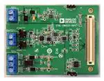
The circuit uses the EVAL-CN0225-SDPZ circuit board and the
EVAL-SDP-CB1Z System Demonstration Platform (SDP)
evaluation board. The two boards have 120-pin mating
connectors, allowing for the quick setup and evaluation of the
circuit’s performance. The EVAL-CN0225-SDPZ board contains
the circuit to be evaluated, as described in this circuit note, and
the SDP evaluation board is used with CN0225 evaluation
software to capture the data from the EVAL-CN0225-SDPZ
circuit board.
Equipment Needed
• PC with a USB port and Windows XP or Vista (32-bit),
or Windows 7 (32-bit)
• EVAL-CN0225-EB1Z circuit evaluation board
• EVAL- SDP-CB1Z SDP evaluation board
• DC Supply: +15 V, –15 V, and +6 V
• Low distortion single-ended or differential signal source,
such as Agilent 81150A or Audio Precision System
Two 2322.
Getting Started
Load the evaluation software by placing the CN0225 Evaluation
Software disc in the CD drive of the PC. Then locate the drive
that contains the evaluation software disc and open the Readme
file. Follow the instructions contained in the Readme file for
installing and using the evaluation software.
Functional Block Diagram
Figure 4 shows a functional block diagram of the test setup. The
PDF file “EVAL-CN0225-SDPZ-SCH” has the detailed
schematics for the CN0225 evaluation board. This file is
contained in the CN0225 Design Support Package:
www.analog.com/CN0225-DesignSupport.
VIN+
SDP
EVAL-CN0225-SDPZ
USB
10058-004
CIRCUIT EVALUATION AND TEST
VIN–
GND +6V
SDP CONA OR CONB
+15V –15V GND
120-PIN SDP CONNECTOR
The reference for the ADC can be changed to the ADR430,
which is 2.048 V. This makes use of a larger percentage of the
input range of the ADC; however, an additional AVDD power
supply for the AD7687 is required.
USB
SIGNAL SOURCE
If 18-bit resolution is needed, the following are also pincompatible members of the PulSAR family: AD7691 (250 kSPS),
AD7690 (400 kSPS), and AD7982 (1 MSPS).
PC
TRIPLE POWER SUPPLY
Figure 4. Test Setup Functional Block Diagram
Setup
Connect the 120-pin connector on the EVAL-CN0225-SDPZ
circuit board to the connector marked “CONA” on the
EVAL-SDP-CB1Z evaluation (SDP) board. Nylon hardware
should be used to firmly secure the two boards, using the
holes provided at the ends of the 120-pin connectors. After
successfully setting the dc output supply to +15 V, -15 V and
+6 V output, turn the power supply off.
With power to the supply off, connect a +15 V power supply to
the pin of J3 marked “+15VA” and a −15 V power supply to the
pin of J3 marked “−15VA” and “GND” to the pin of J3 marked
“AGND”. Connect +6 V to J2 in the same manner. Turn on the
power supply and then connect the USB cable with the SDP
board to the USB port on the PC. Note: Do not connect the
USB cable to the mini USB connect on the SDP board before
turning on the dc power supply for the EVAL-CN0225-SDPZ.
Test
After setting up the power supply and connecting it to the
EVAL-CN0225-SDPZ circuit board, launch the evaluation
software and connect the USB cable from the PC to the USB
mini-connector on the SDP board. The software will be able to
communicate to the SDP board if the Analog Devices System
Development Platform driver is listed in the Device Manager.
Once USB communications are established, the SDP board
can be used to send, receive, and capture serial data from the
EVAL-CN0225-SDPZ board.
The data in this circuit note was generated using an Agilent
81150A differential signal source
Information regarding the SDP board can be found at
www.analog.com/SDP.
Rev. A | Page 4 of 5
�Circuit Note
CN-0225
LEARN MORE
Data Sheets and Evaluation Boards
CN0225 Design Support Package:
www.analog.com/CN0225-DesignSupport
CN-0225 Circuit Evaluation Board (EVAL-CN0225-SDPZ)
SDP User Guide
Ardizzoni, John. A Practical Guide to High-Speed PrintedCircuit-Board Layout, Analog Dialogue 39-09, September
2005.
MT-031 Tutorial, Grounding Data Converters and Solving the
Mystery of “AGND” and “DGND”, Analog Devices.
MT-101 Tutorial, Decoupling Techniques, Analog Devices.
System Demonstration Platform (EVAL-SDP-CB1Z)
AD8295 Data Sheet
AD8275 Data Sheet
AD7687 Data Sheet
AD7687 Evaluation Board
REVISION HISTORY
11/11—Rev. 0 to Rev. A
Change to Circuit Evaluation and Test........................................... 4
10/11—Revision 0: Initial Version
(Continued from first page) Circuits from the Lab circuits are intended only for use with Analog Devices products and are the intellectual property of Analog Devices or its licensors. While you
may use the Circuits from the Lab circuits in the design of your product, no other license is granted by implication or otherwise under any patents or other intellectual property by
application or use of the Circuits from the Lab circuits. Information furnished by Analog Devices is believed to be accurate and reliable. However, "Circuits from the Lab" are supplied "as is"
and without warranties of any kind, express, implied, or statutory including, but not limited to, any implied warranty of merchantability, noninfringement or fitness for a particular
purpose and no responsibility is assumed by Analog Devices for their use, nor for any infringements of patents or other rights of third parties that may result from their use. Analog Devices
reserves the right to change any Circuits from the Lab circuits at any time without notice but is under no obligation to do so.
©2011 Analog Devices, Inc. All rights reserved. Trademarks and
registered trademarks are the property of their respective owners.
CN10058-0-11/11(A)
Rev. A | Page 5 of 5
�