Circuit Note
CN-0292
Devices Connected/Referenced
Circuits from the Lab® reference
designs are engineered and
tested for quick and easy system
integration to help solve today’s
analog, mixed-signal, and RF
design challenges. For more
information and/or support, visit
www.analog.com/CN0292.
AD7176-2
24-Bit, 250 kSPS, Σ-Δ ADC with
20 μs Settling
AD8475
Precision, Selectable Gain, Fully
Differential Funnel Amplifier
ADR4550
Ultralow Noise, High Accuracy,
5.0 V Voltage Reference
ADuM3471
Isolated Switching Regulators
(3/1 Channel Directionality)
ADP7102
20 V, 300 mA, Low Noise,
CMOS LDO Regulator
ADA4898-1
High Voltage, Low Noise,
Low Distortion, Unity Gain
Stable, High Speed Op Amp
ADP7182
−28 V, 200 mA, Low Noise,
Linear Regulator
ADA4096-4
ADG1204
ADP1720
30 V, Micropower, Overvoltage
Protection, RRIO, Quad Op Amp
Low Capacitance, Low Charge
Injection, iCMOS®, ±15 V/±12 V,
4:1 Multiplexer
50 mA, High Voltage,
Micropower Linear Regulator
Completely Isolated, Robust, 4-Channel, Multiplexed Data Acquisition System for
Industrial Level Signals
EVALUATION AND DESIGN SUPPORT
Circuit Evaluation Boards
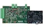
CN-0292 Circuit Evaluation Board (EVAL-CN0292-SDZ)
System Demonstration Platform, SDP-B (EVAL-SDP-CB1Z)
Design and Integration Files
Schematics, Layout Files, Bill of Materials
CIRCUIT FUNCTION AND BENEFITS
The circuit in Figure 1 is a completely isolated, robust, industrial,
4-channel data acquisition system that provides 16-bit, noise
free code resolution and an automatic channel switching rate
of up to 42 kSPS. The channel to channel crosstalk at 42 kSPS
switching is less than 15 ppm FS (less than −90 dB) because of
the unique selection of fast settling components in the multiplexed
signal chain.
The circuit acquires and digitizes standard industrial signal
levels of ±5 V, ±10 V, 0 V to 10 V, and 0 mA to 20 mA. The
input buffers also provide overvoltage protection, thereby
eliminating the leakage errors associated with conventional
Schottky diode protection circuits.
Applications for the circuit include process control (PLC/DCS
modules), battery testing, scientific multichannel instrumentation,
and chromatography.
Rev. 0
Circuits from the Lab reference designs from Analog Devices have been designed and built by Analog
Devices engineers. Standard engineering practices have been employed in the design and
construction of each circuit, and their function and performance have been tested and verified in a lab
environment at room temperature. However, you are solely responsible for testing the circuit and
determining its suitability and applicability for your use and application. Accordingly, in no event shall
Analog Devices be liable for direct, indirect, special, incidental, consequential or punitive damages due
toanycausewhatsoeverconnectedtotheuseofanyCircuitsfromtheLabcircuits. (Continuedonlastpage)
One Technology Way, P.O. Box 9106, Norwood, MA 02062-9106, U.S.A.
Tel: 781.329.4700
www.analog.com
Fax: 781.461.3113
©2014 Analog Devices, Inc. All rights reserved.
�CN-0292
Circuit Note
+16.76V
+V_ISO
TRANSFORMER
100kΩ
+V_ISO
SCHOTTKY
DIODE
FULL WAVE
RECTIFIER
+15V_REG
VIN
VOUT
ADP7102
8.06kΩ
11.3kΩ
ADJ
1kΩ
–V_ISO
GND
+15V_REG
ADA4096-4
+15V_REG
ADG1204
–V_ISO
47Ω
CH1 10nF
–15V_REG +15V_REG
VIN
+5V_REG
VOUT
ADP7182
IN
11.3kΩ
V2 10Ω
47nF
1.8kΩ
–15V_REG
47nF
47Ω
CH4 10nF
+15V_REG
270pF
1kΩ
10Ω
+IN
0.4×
680pF
–IN
ADA4898-1 0.4×
V4 10Ω
+5V_REG
AD8475
2.5kΩ
68pF
47Ω
CH3 10nF
+15V_REG
2.5kΩ
270pF
1kΩ
VOCM
47nF
–15V_REG
10kΩ
+2.5V
EN
A0
A1
X2
VDD2
+5V_EXT
VDD1
VDDA
VOUT
GND2
GND1
ADR4550
GND2
GND1
GND_EXT
GND
+5V
AVDD1,
AVDD2
AIN1
AIN0
10Ω
X1
FB
OC
VIN
GND
+5V_REG
47Ω
V3 10Ω
100kΩ
+15V_REG
1kΩ
GND
CH2 10nF
OUT
ADP7182
ADJ
47nF
+5V_REG
VREG
ADuM3471
REF+
AD7176-2
DGND AVSS
CS
SCLK
DIN
DOUT
VOA
VOB
VOC
VID
VIA
VIB
VIC
VOD
SPI
ISOLATED
SIDE
PROCESSOR
SIDE
10976-001
V1 10Ω
+1.25V
REFOUT
GPIO0
GPIO1
±10V
INPUTS
–15V_REG
Figure 1. Functional Block Diagram of 4-Channel Data Acquisition System (Simplified Schematic: All Connections and Decoupling Not Shown)
VIN
CH1
Signal Path
+FS
C
Four channels of input signals are buffered by the ADA4096-4,
a quad, rail-to-rail, input/output op amp featuring overvoltage
protection against phase reversal or latch-up for inputs of up to
32 V above or below the ±15 V supply rails, which eliminates
the need for additional overvoltage protection circuitry.
The inputs are designed for typical low frequency, industrial
signals of ±10 V. The input buffers provide a high impedance
to the sources and isolate the inputs from the multiplexer switching
transients.
The RC networks on the inputs of the buffers (10 Ω/10 nF)
have a bandwidth of 1.6 MHz and provide high frequency noise
filtering.
The RC networks on the outputs of the ADA4096-4 (47 Ω/47 nF)
isolate the buffers from the multiplexer switching transients.
Figure 2 shows an equivalent circuit. The drain capacitor, CD,
must be charged by the input voltage before switching to the
next channel. There can be as much as 20 V between channels,
and a transient current is generated when the multiplexer switches
to the next channel.
R
VIN
CH2
–FS
VOUT
CD
R
+FS
–FS
C
10976-002
CIRCUIT DESCRIPTION
Figure 2. RC Kickback Isolation Circuit
The ADG1204 multiplexer, featuring low drain capacitance
(