Circuit Note
CN-0314
Devices Connected/Referenced
Circuits from the Lab® reference designs are engineered and
tested for quick and easy system integration to help solve today’s
analog, mixed-signal, and RF design challenges. For more
information and/or support, visit www.analog.com/CN0314.
AD8420
Wide Supply Range, Rail-to-Rail
Output Instrumentation Amplifier
ADR02
Ultracompact, Precision 5.0 V Voltage
Reference
Configurable 4-20 mA Loop Powered Transmitter/Receiver using a Micropower
Instrumentation Amplifier
EVALUATION AND DESIGN SUPPORT
CIRCUIT FUNCTION AND BENEFITS
Circuit Evaluation Boards
CN0314 Evaluation Board (EVAL-CN0314-EB1Z)
Design and Integration Files
Schematics, Layout Files, Bill of Materials
The circuit shown in Figure 1 is a configurable 4 mA-to-20 mA
loop-powered transmitter based on an industry-leading
micropower instrumentation amplifier. Total unadjusted error
is less than 1%. It can be configured with a single switch as
either a transmitter (Figure 1) that converts a differential input
voltage into a current output, or as a receiver (Figure 5) that
converts a 4 mA-to-20 mA current input to a voltage output.
P5-1
ADR02
R4
22.6kΩ
P2-1
+VIN
0V TO 5V
OR
0V TO 10V
ICIRCUIT
5V
R3
11.0kΩ
R1
5.05kΩ
ICIRCUIT + IAMP
195mV
TO
990mV
R2
20.5kΩ
0V TO 10V
0V TO 5V
R5
1kΩ
100µA TO 200µA
IQ1
IAMP
330pF
20kΩ
P3
ILOOP
4mA TO 20mA
+IN
+VS
+
AD8420
3.3nF
LOOP
SUPPLY
12V TO 36V
Q1
ZXT13N50DE6
VOUT
−
FB
REF
0V
–IN
−VS
250Ω
RLOOP
ICIRCUIT
330pF
NOTE: R1, R2, R3, R4 AND R5 ARE 0.1%
IQ1
100µA
TO
200µA
3.9mA
TO
19.8mA
+
VR9
–
R9
50Ω
0.1%
IAMP
VR9: 195mV TO 990mV
P5-2
ILOOP
LOOP
GROUND
11284-001
20kΩ
P2-2
−VIN
Figure 1. Robust Loop Powered Configurable Transmitter Circuit with 4 mA-to-20 mA Output
Rev. 0
Circuits from the Lab® reference designs from Analog Devices have been designed and built by Analog
Devices engineers. Standard engineering practices have been employed in the design and
construction of each circuit, and their function and performance have been tested and verified in a lab
environment at room temperature. However, you are solely responsible for testing the circuit and
determining its suitability and applicability for your use and application. Accordingly, in no event shall
Analog Devices be liable for direct, indirect, special, incidental, consequential or punitive damages due
toanycausewhatsoeverconnectedtotheuseofanyCircuitsfromtheLabcircuits. (Continuedonlastpage)
One Technology Way, P.O. Box 9106, Norwood, MA 02062-9106, U.S.A.
Tel: 781.329.4700
www.analog.com
Fax: 781.461.3113
©2014 Analog Devices, Inc. All rights reserved.
�CN-0314
Circuit Note
The design is optimized for precision, low noise and low power
industrial process control applications. The circuit can accept
0 V to 5V or 0 V to 10 V input range as a transmitter. As a
receiver it can provide 0.2 V to 2.3 V or 0.2 V to 4.8 V output
range compatible with ADCs using 2.5 V or 5 V references. The
supply voltage can range from 12 V to 36 V as a transmitter and
7 V to 36 V as a receiver.
Since the circuit is configurable, a single hardware design can be
used as a backup for both transmitter and receiver at the same
time, minimizing customer inventory requirements.
CIRCUIT DESCRIPTION
The circuit features the AD8420, an instrumentation amplifier
based on an indirect current feedback architecture. Because of
this architecture, the AD8420 has excellent input and output
characteristics. Unlike conventional instrumentation amplifiers,
the AD8420 can easily amplify signals at or even slightly below
ground without requiring dual supplies. The AD8420 has railto-rail output voltage swing that is completely independent of
the input common-mode voltage. This exempts the AD8420
from the restrictions caused by interaction between the
common-mode input and output voltage associated with most
conventional instrumentation amplifier architectures. The
flexible input and output characteristics, together with
micropower consumption (80 µA maximum for 0 V input) and
wide supply range, make the AD8420 ideal for flexible low
power industrial applications.
Transmitter Configuration
Figure 1 shows the simplified schematic for the 4mA-to-20mA
transmitter configuration. The circuit only consumes around
1 mA of current, which makes it suitable for loop-powered
applications. The transmitter has input ranges of 0 V to 5 V and
0 V to 10 V, which can be selected using Jumper P3. The input
voltage range is then scaled down to 0.195 V to 0.990 V range
since the differential input voltage of AD8420 is limited to
maximum of 1 V.
The input to the AD8420 has a differential mode noise filter
(40 kΩ/3.3 nF) with a 1.2 kHz bandwidth and a common-mode
noise filter (20 kΩ/330 pF) with a 24 kHz bandwidth.
The indirect current feedback architecture of AD8420 forces the
differential input voltage of the amplifier to appear between its
FB and REF pins. The transistor Q1 then translates the 0.195 V
to 0.990 V range into 3.9 mA to 19.8 mA flowing through the
R9 50 Ω sense resistor.
The current through the R9 sense resistor includes the circuit
current and the Q1 current, but not the AD8420 current, IAMP.
The unique architecture of the AD8420 makes its supply
current predictable from 100 µA to 200 µA for a 0.195 V to
0.990 V input applied between +IN and −IN. This supply
current will add to the current through R9, bringing the total
output loop current to 4 mA-to-20 mA. Therefore, the total
current in the loop is given by the equation:
I LOOP = I AMP + I R9
In order for the circuit to operate properly, the total circuit
supply voltage must be greater than 7 V to provide sufficient
headroom for the ADR02 voltage reference.
VLOOP SUPPLY > 7 V + RLoadILoop(max)
For RLOOP of 250 Ω,
VLOOP SUPPLY > 7 V + (250 Ω)(20 mA)
Therefore,
VLOOP SUPPLY > 12 V
The loop supply voltage is also limited to 36 V maximum.
An advantage of AD8420 is its high impedance reference pin
that eliminates the need for an additional op-amp to drive it,
thus, saving power, cost and space in the transmitter circuit.
It is important for proper loop operation that the circuit board
ground and the loop ground are not connected except for the
R9, 50 Ω sense resistor.
Selection of Scaling Resistors
The differential input voltage range of AD8420 is limited to
maximum of ±1V. Hence, to be able to accept higher industrial
input voltage range, the circuit makes use of a scaling resistor
network to translate the 0 V to 5 V or 0 V to 10 V input into
0.195 V to 0.990 V. The following equations use nodal analysis
to obtain the values for R1, R2, R3, and R4 in the circuit:
VIN MIN – 0.195 V V REF – 0.195 V 0.195 V
(1)
+
=
R1
R2
R5
VIN MAX – 0.990 V
+
V REF – 0.990 V
R1
=
0.990 V
R2
(2)
R5
where:
VREF = 5 V
R5 = 1 kΩ
For 0 V to 5 V input range, Equation 1 and Equation 2 lead to
Equation 3 and Equation 4, respectively.
0 V – 0.195 V 5 V – 0.195 V 0.195 V
(3)
+
=
R1
R2
1 kΩ
5 V – 0.990 V
+
5 V – 0.990 V
R1
=
0.990 V
R2
(4)
1 kΩ
Solving for R1 and R2 using Equation 3 and Equation 4:
R1 = 5044 Ω
R2 = 20564 Ω
For 0 V to 10 V input range, Equation 1 and Equation 2 results
to Equation 5 and Equation 6, respectively.
0 V – 0.195 V 5 V – 0.195 V 0.195 V
(5)
+
=
R3
R4
1 kΩ
10 V – 0.990 V
R3
Rev. 0 | Page 2 of 8
+
5 V – 0.990 V
R4
=
0.990 V
1 kΩ
(6)
�Circuit Note
CN-0314
Again, solving for the corresponding scaling resistors:
Total Transmitter Circuit Accuracy
R3 =11088 Ω
R4 =22603 Ω
In the practical circuit, the nearest EIA standard 0.1% resistor
values must be chosen, resulting in fixed offset error. The
resistors supplied with the EVAL-CN0314-EB1Z board are as
follows:
R1 = 5050 Ω and R2 = 20500 Ω
R3 = 11000 Ω and R4 = 22600 Ω
With these values supplied with the board, the offset errors due
to the resistor values can be computed using the following
equations:
For 0 V to 5 V inputs, VREF = 5 V, R1 = 5.05 kΩ, R2 = 20.5 kΩ,
and R5 = 1 kΩ.
Offset Error (%FSR) =
VIN VREF
( R1 )( R2 )( R5 )
+
R2
R1
− IQ1 ( ideal )
× 100%
[( R1 )( R2 ) + ( R2 )( R5 ) + ( R1 )( R5 )] 50 Ω
mA
16
(7)
Offset Error (%FSR) = 0.078% at VIN = 0 V; IQ1 = 3.9 mA
Offset Error (%FSR) = −0.033% at VIN = 5 V; IQ1 = 19.8 mA
Consequently, for 0 V to 10 V inputs, VREF = 5 V, R3 = 11 kΩ,
R4 = 22.6 kΩ, and R5 = 1 kΩ:
A good approximation of the total error contributed by the
resistor tolerances is to assume that each of the critical resistors
contributes equally to the total error. The four critical resistors
are R1 or R3, R2 or R4, R5 and R9. Worst-case tolerance build
up of 0.1% resistors yield a total resistor error of 0.4% maximum. If
rss errors are assumed, the total rss error is 0.1√4 = 0.2%.
The maximum and rss errors due to the active components in
the system using the A grade for AD8420 and B grade for levels
of ADR02 are shown in the table below.
Table 1. Errors Due to Active Components
Error Component
AD8420-A
ADR02-B
RSS FS Error
Max FS Error
Error
Offset
Offset
Error Value
250 µV
0.06%
Error %FSR
0.03%
0.015%
0.034%
0.045%
Adding the worst case resistor tolerance error of 0.4% to the
worst-case errors due to the offsets of active components yields:
Full Scale Error = 0.4% + 0.045% = 0.445%
These errors assume that ideal resistors were selected and the
errors resulted from their tolerances.
Actual error data from the circuit is shown in Figure 3 and
Figure 4 with a loop supply = 25 V. The total output error
(%FSR) is calculated by taking the difference between the
measured output current and the ideal output current, dividing
by the FSR (16 mA), and multiplying the result by 100.
0.10
Offset Error (%FSR) =
VIN VREF
( R3 )( R4 )( R5 )
+
R4
R3
− IQ1 ( ideal )
× 100%
[( R3 )( R4 ) + ( R4 )( R5 ) + ( R3 )( R5 )] 50 Ω
16 mA
TOTAL ERROR (%FSR)
0.05
0
–0.05
–0.10
–0.15
Offset Error (%FSR) = −0.013% at VIN = 0 V; IQ1 = 3.9 mA
Offset Error (%FSR) = 0.718% at VIN = 10 V; IQ1 = 19.8 mA
To minimize this offset error, it is also possible to use
combination of two 0.1% values to come closer to the calculated
resistor values.
–0.20
0
0.5
1.0
1.5
2.0
2.5
3.0
3.5
VOLTAGE INPUT (V)
4.0
4.5
5.0
11284-002
(8)
Figure 2. Total Transmitter Error (% FSR) vs. Input Voltage (0 V to 5 V Range)
Rev. 0 | Page 3 of 8
�TOTAL ERROR (%FSR)
CN-0314
Circuit Note
0.7
Receiver Configuration
0.6
The simplified receiver configuration is illustrated in Figure 4.
The receiver circuit translates the current signal into a voltage
level that is compatible with most single-ended input ADCs
operating on either 2.5 V or 5 V references.
0.5
0.4
0.3
0.2
0.1
–0.1
0
1
2
3
4
5
6
7
VOLTAGE INPUT (V)
8
9
10
11284-003
0
Figure 3. Total Transmitter Error (% FSR) vs. Input Voltage (0 V to10 V Range)
VCC
7V TO 36V
P5-1
J1
VOUT
P5-2
ADR02
R12
23.7kΩ
20kΩ
R13
4.53kΩ
R14
24.3kΩ
330pF
P1-1
IIN 0.2V TO 1V
R11
1.58kΩ
+IN
P4
+VS
0.2V TO 2.3V
0.2V TO 4.8V
4mA TO 20mA
P1-2
20kΩ
0V
AD8420
3.3nF
VOUT
FB
–IN
REF
−VS
R10
1kΩ
330pF
NOTE: R10, R11, R12, R13 AND R14 ARE 0.1%
Figure 4. Simplified Schematic for 4 mA-to-20 mA Receiver Configuration
Rev. 0 | Page 4 of 8
J2
11284-004
R6
50Ω
0.1%
�Circuit Note
CN-0314
Resistor R6 is used to sense the 4 mA-to-20 mA signal and
convert it into a 0.2 V to 1 V input voltage to the amplifier. The
input voltage is then reflected across the FB and REF pins of the
amplifier. Unlike most direct-gain receivers with an output
voltage range of 1 V to 5 V, the circuit uses the ADR02 together
with gain and scaling resistors to provide an output of 0.2 V to
4.8 V. This maximizes the input dynamic range of ADCs with
5 V references. The extra headroom ensures linearity across the
entire input signal range. The receiver circuit can also be
configured using Jumper P4 to give an output of 0.2 V to 2.3 V
for ADCs that use 2.5 V references.
The key advantage of AD8420 for this application is that it can
sense the current near ground without exceeding the input
range or running into common-mode restrictions, unlike many
other single supply instrumentation amplifiers. Additionally,
the AD8420 provides gain and level shifting capability so that it
does not waste ADC input range as would be the case with
simple resistive dividers.
Thus,
R13 = 4560 Ω
R14 = 24000 Ω
The resistor supplied on the circuit board is the value nearest
EIA standard 0.1% resistor that is obtainable from and available
with the suppliers. Thus, actual values of the resistor supplied
on the board are as follows:
R11 = 1580 Ω and R12 = 23700 Ω
R13 = 4530 Ω and R14 = 24300 Ω
With these values supplied with the board, the offset errors due
to the resistor values are as follows:
For a 0.2 V to 2.3 V output range, VREF = 5 V, R11 = 1580 Ω,
R12 = 23700 Ω, and R10 = 1 kΩ.
Offset Error (%FSR) =
R11
R11 R11
– VREF
– V OUT _ IDEAL
–
VFB 1 +
R10 R12
R12
V OUT _ MAX – V OUT _ MIN
Selection of Gain and Scaling Resistors
The gain of the AD8420 is usually set by the ratio of two
resistors (R11 and R10). However, the circuit utilizes ADR02 to
take advantage of the extra 20% of the range that is wasted with
direct gain on the low side. The equations below show how to
get the value of the gain and scaling resistors for the desired
output voltage ranges.
VOUT MIN – 0.200 V VREF – 0.200 V 0.200 V
+
=
R11
R12
R10
(9)
VOUT MAX – 1 V VREF – 1 V 1 V
+
=
R11
R12
R10
(15)
Offset Error (%FSR) = −0.190% at VFB = 0.2 V; VOUT_IDEAL
= 0.2 V
Offset Error (%FSR) = 0.635% at VFB = 1 V; VOUT_IDEAL =
2.3 V
For a 0.2 V to 4.8 V output range, VREF = 5 V, R13 = 4530 Ω,
R14 = 24300 Ω, and R10 = 1 kΩ.
Offset Error (%FSR) =
(10)
R13
R13 R13
– V OUT _ IDEAL
– VREF
–
VFB 1 +
R10 R14
R14
V OUT _ MAX – V OUT _ MIN
where:
VREF = 5 V
R10 = 1 kΩ
For 0.2 V to 2.3 V output range:
0.2 V – 0.200 V
+
5 V – 0.200 V
R11
2.3 V – 1 V
=
R12
+
5V – 1 V
R11
(11)
1 kΩ
Offset Error (%FSR) = 0.243% at VFB = 0.2 V; VOUT_IDEAL =
0.2 V
It is also possible to use combination of two 0.1% values to
come closer to the calculated values minimize this offset error.
R11 = 1560 Ω
R12 = 24000 Ω
Total Receiver Circuit Accuracy
For 0.2 V to 4.8 V output range,
+
5 V – 0.200 V
R13
4.8 V – 1 V
R13
R14
+
5V – 1 V
R14
=
Offset Error (%FSR) = −0.341% at VFB = 1 V; VOUT_IDEAL =
4.8 V
(12)
This gives us resistor values of
0.2 V – 0.200 V
× 100%
(16)
1 kΩ
1V
=
R12
0.200 V
× 100%
=
0.200 V
(13)
1 kΩ
1V
1 kΩ
(14)
A good approximation of the total error contributed by the
resistor tolerances is to assume that each of the critical resistors
contributes equally to the total error. The four critical resistors
are R11 or R13, R12 or R14, R6 and R10. Worst-case tolerance
build up of 0.1% resistors yield a total resistor error of 0.4%
maximum. If rss errors are assumed, the total rss error is
0.1√4 = 0.2%.
Rev. 0 | Page 5 of 8
�CN-0314
Circuit Note
The maximum and rss errors due to the active components in
the system using the A grade for AD8420 and B grade for levels
of ADR02 are shown in the table below.
0.2
TOTAL ERROR (%FSR)
0.1
Table 2. Errors Due to Active Components
Error
Offset
Offset
Gain
Error Value
0.06%
250 µV
0.05%
Error % FSR
0.01%
0.01%
0.05%
0.014%
0.05%
0.064%
0.02%
0.05%
0.07%
Adding the worst case resistor tolerance error of 0.4% to the
worst-case errors due to the active components yields:
Full Scale Error = 0.4% + 0.07% = 0.47%
These errors assume that ideal resistors were selected, and the
errors resulted from their tolerances.
Actual error data for the receiver circuit is shown in Figure 5
and Figure 6 with VCC = 25 V. The total output error (% FSR) is
calculated by taking the difference between the measured
output voltage and the ideal output current, dividing by the FSR
of the output voltage, and multiplying the result by 100.
0.4
TOTAL ERROR (%FSR)
0.3
–0.1
–0.2
–0.3
–0.4
–0.5
–0.6
0
2
4
6
8
10
12
14
CURRENT INPUT (mA)
16
18
20
11284-006
Error Component
ADR02-B
AD8420-A
AD8420-A
RSS FS Offset
RSS FS Gain
RSS FS Error
Max FS Offset
Max FS Gain
Max FS Error
0
Figure 6. Total Receiver Error (%FSR) vs. Input Voltage (4 mA-to-20 mA
Range) for 0.2 V to 4.8 V Output Range
A design support package for the EVAL-CN0314-EB1Z
transmitter/receiver board including complete schematics, bill
of materials, and layout files, can be found at
http://www.analog.com/CN0314-DesignSupport.
COMMON VARIATIONS
The circuit is proven to work with good stability and accuracy
with component values shown. Other voltage references and inamp can be used in this configuration for other various
applications for this circuit.
The AD8237, a micropower, zero drift, true rail-to-rail
instrumentation amplifier can also be used for low supply
voltage versions of this circuit configuration.
The ADR4550, high precision, low power, low noise voltage
references can be used to replace the ADR02 for a low voltage
supply applications.
0.2
0.1
0
–0.1
–0.3
0
2
4
6
8
10
12
14
CURRENT INPUT (mA)
16
18
20
11284-005
–0.2
Figure 5. Total Receiver Error (%FSR) vs. Input Current (4 mA-to-20 mA
Range) for 0.2 V to 2.3 V Output Range
Rev. 0 | Page 6 of 8
�Circuit Note
CN-0314
CIRCUIT EVALUATION AND TEST
Equipment Required
EVAL-CN0314-EB1Z evaluation board
Agilent E3631A dual dc power supply or equivalent
Yokogawa 2000 precision dc power supply or equivalent
Agilent 3458 precision multimeter or equivalent
Test Setup Configuration and Tests
For the test setup of the transmitter configuration (Figure 8), a
Yokogawa 2000 precision dc source was used to generate a 0 V
to 5 V or 0 V to 10 V differential input ranges. The S1 switch
must be placed in the “V-I” position to configure the circuit as a
transmitter
POWER SUPPLY
V+
P2-1
COM
P2-2
P5-1
EVAL-CN0314-EB1Z
P5-2
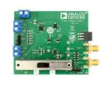
Figure 9. Photo of EVAL-CN0314-EB1Z Board
Switch and Jumper Settings for 4 mA-to-20 mA Transmitter
For the transmit configuration shown in Figure 1, Switch S1
should be put in the “V-I” position. Jumper P3 should be put in
the “0–10V” position for an input range of 0 V to 10 V, and in
the “0–5V” position for an input range of 0 V to 5 V. See also
the photo of the evaluation board in Figure 9.
VOUT
Switch and Jumper Settings for 4 mA-to-20 mA Receiver
COM
For the receiver configuration shown in Figure 4, Switch S1
should be put in the “I-V” position. Jumper P4 should be put in
the “0.2–2.3V” position for an output voltage of 0.2 V to 2.3 V,
and in the “0.2–4.8V” position for an output voltage of 0.2 V to
4.8 V. See also the photo of the evaluation board in Figure 9.
CURRENT METER
COM
11284-007
PRECISION
VOLTAGE
SOURCE
11284-009
The circuit was tested using the test setup shown in Figure 7
and Figure 8. The Agilent 3631A was set to 25 V to serve as the
power supply of the board. The Agilent 3458 multimeter was
used to measure the actual current or voltage output of the
evaluation board. A photo of the EVAL-CN0314-EB1Z is shown
in Figure 9.
I
Figure 7. Functional Block Diagram of Test Setup for the Transmitter
For the test setup of the receiver configuration (Figure 9), a
second EVAL-CN0314-EB1Z was used to produce a 4 mA-to20 mA input current. A precision current source can be used if
desired. The S1 switch must be placed in the “I-V” position to
configure the circuit as a receiver.
POWER SUPPLY
P5-1
VOUT
P5-2
COM
EVAL-CN0314-EB1Z
VOLTAGE METER
P1-1
P1-2
VOUT
V
J1
COM
COM
11284-008
CURRENT IOUT
SOURCE
COM
Figure 8. Functional Block Diagram of Test Setup for the Receiver
Rev. 0 | Page 7 of 8
�CN-0314
Circuit Note
LEARN MORE
CN-0314 Design Support Package:
http://www.analog.com/CN0314-DesignSupport
MT-031 Tutorial, Grounding Data Converters and Solving the
Mystery of AGND and DGND. Analog Devices.
MT-035 Tutorial, Op Amp Inputs, Outputs, Single-Supply, and
Rail-to-Rail Issues. Analog Devices.
MT-065 Tutorial, In-Amp Noise. Analog Devices.
MT-066 Tutorial, In-Amp Bridge Circuit Error Budget Analysis.
Analog Devices.
MT-087 Tutorial, Voltage References. Analog Devices.
MT-101 Tutorial, Decoupling Techniques. Analog Devices.
Voltage Reference Wizard Design Tool.
Data Sheets and Evaluation Boards
CN-0314 Circuit Evaluation Board (EVAL-CN0314-EB1Z)
AD8420 Data Sheet
ADR02 Data Sheet
REVISION HISTORY
3/14—Revision 0: Initial Version
(Continued from first page) Circuits from the Lab reference designs are intended only for use with Analog Devices products and are the intellectual property of Analog Devices or its licensors.
While you may use the Circuits from the Lab reference designs in the design of your product, no other license is granted by implication or otherwise under any patents or other intellectual
property by application or use of the Circuits from the Lab reference designs. Information furnished by Analog Devices is believed to be accurate and reliable. However, Circuits from the
Lab reference designs are supplied "as is" and without warranties of any kind, express, implied, or statutory including, but not limited to, any implied warranty of merchantability,
noninfringement or fitness for a particular purpose and no responsibility is assumed by Analog Devices for their use, nor for any infringements of patents or other rights of third parties
that may result from their use. Analog Devices reserves the right to change any Circuits from the Lab reference designs at any time without notice but is under no obligation to do so.
©2014 Analog Devices, Inc. All rights reserved. Trademarks and
registered trademarks are the property of their respective owners.
CN11284-0-3/14(0)
Rev. 0 | Page 8 of 8
�


 工商网监
湘ICP备2023018690号
工商网监
湘ICP备2023018690号
