Circuit Note
CN-0342
Devices Connected/Referenced
Circuits from the Lab® reference designs are engineered and
tested for quick and easy system integration to help solve today’s
analog, mixed-signal, and RF design challenges. For more
information and/or support, visit www.analog.com/CN0342.
ADuM3190
2.5 kV rms Isolated Error Amplifier
ADP1621
Constant-Frequency, Current-Mode
Step-Up DC-to-DC Controller
Flyback Power Supply Using a High Stability Isolated Error Amplifier
EVALUATION AND DESIGN SUPPORT
The entire circuit operates from 5 V to 24 V, allowing it to be
used with standard industrial and automotive power supplies.
The output capability of the circuit is up to 1 A with a 5 V input
and 5 V output configuration.
Circuit Evaluation Board
CN-0342 Circuit Evaluation Board (EVAL-CN0342-EB1Z)
Design and Integration Files
Schematics, Layout Files, Bill of Materials
This solution can be adapted for use in applications where higher
dc input voltages are used to create lower voltage isolated supplies
with good efficiency and a small form factor. Examples include
10 W to 20 W telecommunication and server power supplies,
where power efficiency and printed circuit board (PCB) density
are important, and −48 V supplies are common.
CIRCUIT FUNCTION AND BENEFITS
The circuit shown in Figure 1 is an isolated, flyback power
supply that uses a linear isolated error amplifier to supply the
feedback signal from the secondary side to the primary side.
Unlike optocoupler-based solutions, which have a nonlinear
transfer function that changes over time and temperature, the
linear transfer function of the isolated amplifier is stable and
minimizes offset and gain errors when transferring the feedback
signal across the isolation barrier.
VOUT
5V TO 24V
T1
C26
C25
C14
47µF
47µF
100µF
R12
820Ω
C21
220nF
D1
R19
390Ω
C23
C24
C3
47µF
47µF
100µF
5V
R4
100kΩ
Q2
R18
0Ω
IN
SDSN
CS
GND
COMP PIN
GATE
FB
FREQ PGND
ADP1621
R3
51kΩ
R5
82Ω
D2
Q3
R16
0Ω
R6
100kΩ
C17
0.1µF
R2
47kΩ
R1
2kΩ
R20
0Ω
VDD1
VDD2
ADuM3190
REF
REFOUT
+IN
EAOUT
–IN
C10
1nF
COMP
GND1
GND2
R19
15kΩ
C9
2.2nF
11763-001
VIN
Figure 1. Simplified Schematic of Flyback Power Supply Circuit
Rev. 0
Circuits from the Lab reference designs from Analog Devices have been designed and built by Analog
Devices engineers. Standard engineering practices have been employed in the design and
construction of each circuit, and their function and performance have been tested and verified in a lab
environment at room temperature. However, you are solely responsible for testing the circuit and
determining its suitability and applicability for your use and application. Accordingly, in no event shall
Analog Devices be liable for direct, indirect, special, incidental, consequential or punitive damages due
toanycausewhatsoeverconnectedtotheuseofanyCircuitsfromtheLabcircuits. (Continuedonlastpage)
One Technology Way, P.O. Box 9106, Norwood, MA 02062-9106, U.S.A.
Tel: 781.329.4700
www.analog.com
Fax: 781.461.3113
©2014 Analog Devices, Inc. All rights reserved.
�CN-0342
Circuit Note
CIRCUIT DESCRIPTION
The average transformer primary side current, ILAVG, is given by
The isolation amplifier is the ADuM3190, which includes a
1.225 V voltage reference and an error amplifier with 10 MHz
unity-gain bandwidth product. An external resistive divider
(R1, R2, R3, and R4) and compensation network (R9, C9, and
C10) complete the analog feedback loop.
The input supply range of the ADuM3190 is 3.0 V to 20 V on
both sides, and internal low dropout regulators provide stable
supplies for the voltage reference, error amplifier, and analog
isolator. The ADuM3190 is compatible with the Distributedpower Open Standards Alliance (DOSA) output voltage trim
method.
The ADP1621 provides pulse-width modulation (PWM)
control for the flyback power supply. The internal 5.5 V shunt
regulator provides the capability of high supply input voltage
with the addition of an external NPN transistor (Q2). The
ADP1621 also provides lossless current sensing for current
mode operation, providing excellent line and load transient
response.
Setting the Output Voltage
The output voltage is set through a voltage divider from VOUT to
the −IN pin of ADuM3190. The feedback resistor ratio sets the
output voltage of the system. Using the internal voltage reference in
the ADuM3190, the regulation voltage at the −IN pin is 1.225 V.
VOUT
I LAVG =
where:
ILOAD is the load current.
D is the duty cycle under maximum load current.
NS/NP is the turn ratio of the transformer.
The output voltage is
VOUT × (1 − D) ×
The peak-to-peak primary inductor ripple current is inversely
proportional to the inductor value.
∆I L =
The ADuM3190 provides an internal 1.225 V voltage reference
specified for ±1% accuracy over the −40°C to +125°C temperature
range. The reference voltage output pin (REFOUT) can be connected
to the +IN pin of the error amplifier to set the output voltage.
When higher accuracy or a special output voltage is required, and
a different reference voltage must be used, the +IN pin can also
be connected to an external reference
For this design example, the following parameters were used:
•
•
•
•
•
VIN = 5 V
VOUT = 5 V
IOUTMAX = 1 A
fSW = 200 kHz
Transformer turn ratio = 1:1
f SW × L
where:
fSW is the switching frequency.
L is the primary inductor value.
Assuming continuous conduction mode (CCM) operation, the
primary inductor current is given by
Voltage Reference
The transformer choice is important because it dictates the
primary inductor current ripple.
VIN × D
VIN × D
I LOAD N S
×
+
1 − D N P 2 × f SW × L
Assuming the primary ripple current is 50% of the average current
on the transformer primary side, a reasonable choice for the
inductor value is
For a 5 V output configuration, the resistor divider values are
R1 = 2 kΩ, R2 = 47 kΩ, R3 = 51 kΩ, and R4 = 100 kΩ.
Transformer Selection
NP
= VIN × D
NS
The duty cycle (D) is 50% because the output and input are both
5 V, and the transformer turn ratio is 1:1.
I LPK =
R4 + R3
= 1.225 V × 1 +
R1
+
R2
I LOAD N S
×
1 − D NP
L=
VIN × D × (1 − D)
0.5 × f SW × I LOAD
×
5 V × 0.5 (1 − 0.5)
NP
=
= 12.5 μH
N S 0.5 × 200 kHz × 1 A
The transformer used in this design is a 1:1 turn ratio transformer
with 16 µH primary side inductance (Halo Electronics, Inc.,
TGB01-P099EP13LF).
Compensation Network
In a flyback topology power supply, the output load resistance, the
output capacitor, and its effective series resistance (ESR) add a zero
and a pole at frequencies that are dependent on the component
type and values. There is also a right half plane (RHP) zero in
the control-to-output transfer function. Because the RHP zero
reduces the phase by 90°, the frequency of 0 dB gain (crossover
frequency) is lower than the RHP zero.
With the ADuM3190 providing the error amplifier, a Type II
compensation network can be provided from the −IN pin to the
COMP pin to compensate for the control loop for stability. The
compensation network values depend on the selected components.
Rev. 0 | Page 2 of 5
�Circuit Note
CN-0342
Insulation and Safety
The zeros and poles of a Type II compensation network are
derived as follows:
f ZERO
The ADuM3190 is packaged in a small, 16-lead QSOP package
for a 2.5 kV rms isolation voltage rating.
1
2 R9 C9
f POLE
Safety specifications for the ADuM3190 are shown in Table 1.
C10 C9
Table 1. Safety Specifications for the ADuM3190
2 R9 C10 C9
In this particular design, the compensation network is set by
R9 = 15 kΩ, C9 = 2.2 nF, and C10 = 1 nF.
The zero and the pole provided by this compensation network
are fZERO = 4.8 kHz and fPOLE = 15.4 kHz. Increasing the zero and
pole frequency improves the load transient response but decreases
the phase margin of the feedback loop and can cause instability
in the power supply.
Parameter
Rated Dielectric Insulation Voltage
Minimum External Air Gap (Clearance)
Minimum External Tracking (Creepage)
Minimum Internal Gap (Internal Clearance)
Tracking Resistance (Comparative Tracking
Index)
Isolation Material Group
Value
2500
3.8 min
3.1 min
0.017 min
>400
Unit
V rms
mm
mm
mm
V
II
COMMON VARIATIONS
Snubber Network
When the power MOSFET (Q3) is turned off, there is a high
voltage spike on the drain due to the transformer leakage
inductance. This excessive voltage can overstress the power
MOSFET and lead to a reliability issue or damage. Therefore, it
is necessary to use an additional network to clamp the voltage.
The resistor, capacitor, and diode (R19, C21, and D2) snubber
network absorbs the current in the leakage inductance by turning
on the snubber diode when the MOSFET drain voltage exceeds
the cathode voltage of D2.
The ADP1621 operates in lossless mode with the drain of the
power MOSFET connected to the CS pin. In a practical design,
limit the voltage at the CS pin to an absolute maximum of 33 V, and
a practical maximum of 30 V to maintain accuracy. If the measured
peak voltage exceeds 30 V, or if a more accurate current limit is
desired, connect the CS pin to an external current sense resistor
in the source of the MOSFET.
Primary Side Power Supply
The ADP1621 supply voltage range is 2.9 V to 5.5 V, and the
ADuM3190 supply voltage range is 3.0 V to 20 V. To work
with a 5 V to 12 V input voltage supply, a small-signal NPN
transistor (Q2) can be used as a voltage regulator.
For higher input voltages, the current sense resistor must be used
with a current control loop. Change the R20 resistor from 0 Ω
to the value required by the application. For the 1 A output
configuration, choose a sense resistor value of 50 mΩ. According to
the internal current feedback loop in the ADP1621, the maximum
PWM duty cycle of switching is reduced when the current sensing
voltage rises. If the sense resistor value is too high, the duty cycle of
the switching is limited; the maximum output current is then
also limited under the specific output voltage. The ADP1621
compensation pin (COMP) has a 0 V to 2 V effective input voltage
range. It is recommended to limit the voltage on the CS pin to
less than 0.1 V to guarantee an adequate switching duty cycle.
When working with an input voltage less than 5 V, bypass the
input regulation transistor by shorting the jumper between the
collector and the emitter.
For applications such as telecommunication or server power
supplies with a −48 V input, regulate the supply voltage for the
primary side controller to +5 V. The NPN transistor Q2 needs a
higher VCE breakdown voltage, and the power MOSFET Q3 needs
a higher VDS (100 V, VDSMAX). In addition, change the diode in
the RCD snubber circuit, D2, to a 70 V reverse voltage rating.
To reduce the current on the internal regulator in the ADP1621,
increase R12 to 1.5 kΩ.
The IN pin of ADP1621 has a 5.5 V internal voltage regulator
and is connected to the base node of the NPN transistor Q2.
This connection biases Q2 so that the emitter node can be
regulated to 5.5 V − 0.7 V = 4.8 V, which can be used as the
power supply voltage for the ADP1621 (PIN) and the
ADuM3190 (VDD1).
Table 2 summarizes the alternative components selected for
different input voltage configurations.
Table 2. Component Values for Different Configurations
Secondary Side Power Supply
The ADuM3190 has a 3.0 V to 20 V supply voltage range on the
secondary side (VDD2), with an internal regulator providing a
3.0 V operating voltage. If VOUT is set higher than 20 V, add an
external voltage regulator to provide the specified VDD2 voltage.
Input Voltage
Q2
Q3
D2
R12
5 V to 7 V
PMST2369
NTD18N06L
MBR0540T1
390 Ω
7 V to 24 V
PMST2369
NTD18N06L
MBR0540T1
820 Ω
24 V to 48 V
BC846
NVD6824NL
MMSD701T1
1.5 kΩ
A complete design support package, including the schematics,
layouts, and bill of materials, is available at
www.analog.com/CN0342-DesignSupport.
Rev. 0 | Page 3 of 5
�CN-0342
Circuit Note
Performance Results
Figure 2 shows the measured efficiency with three different
input voltages: 5 V, 12 V, and 24 V.
Figure 4. 100 mA to 900 mA Load Transient Response
Figure 2. Flyback Circuit Output Efficiency vs. Load Current for
Input Voltages of 5 V, 12 V, and 24 V
Figure 3 shows the output voltage over a temperature range
from −40°C to +125°C. The total output voltage error over this
range is less than ±20 mV (±0.4%).
Figure 5. 900 mA to 100 mA Load Transient Response
Figure 3. Flyback Circuit Output Voltage vs. Temperature
Figure 4 and Figure 5 show the transient response for increasing
and decreasing load current. The transient response time is
32 µs for a load current increase from 100 mA to 900 mA, and
45 µs for a load current decrease from 900 mA to 100 mA.
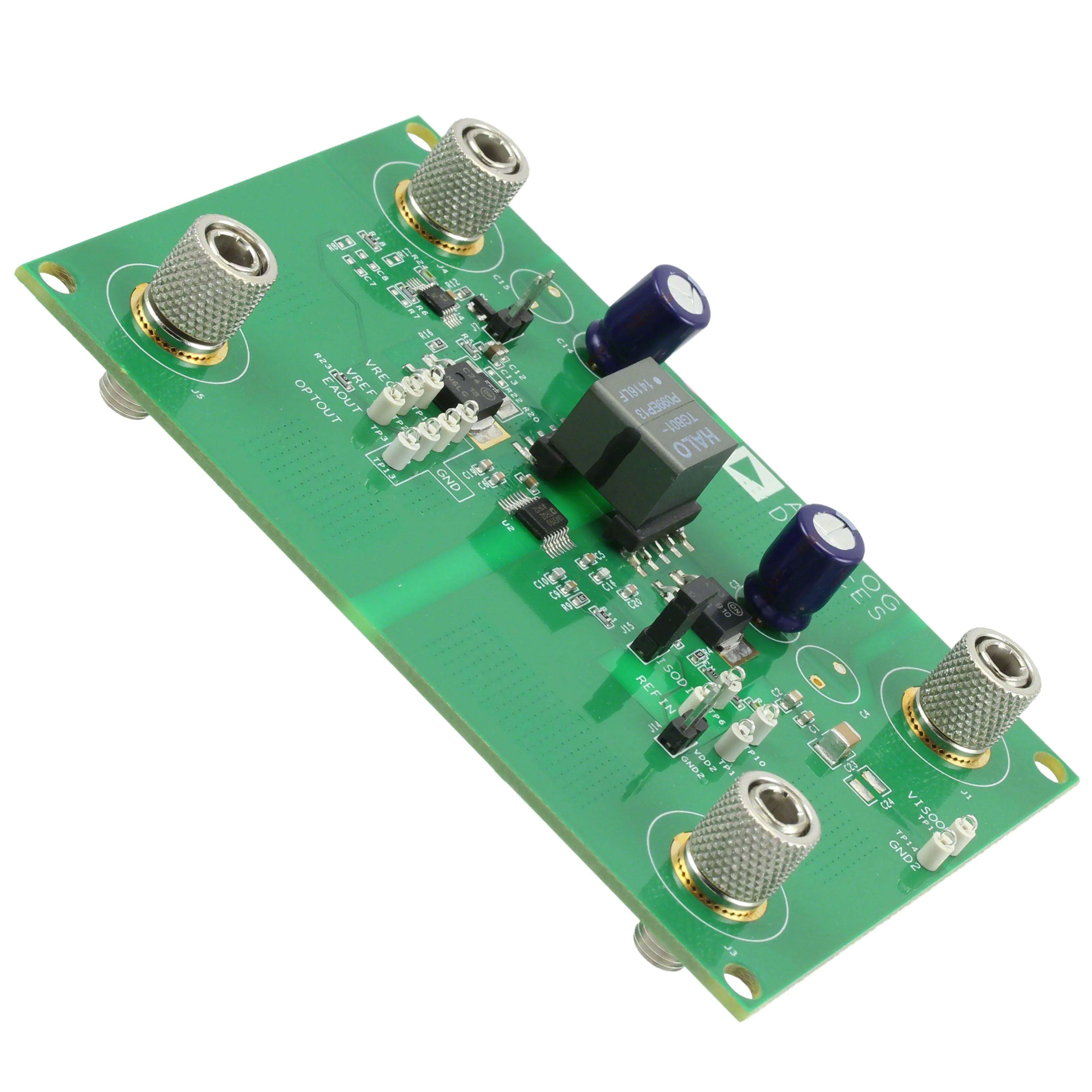
A photograph of the EVAL-CN0342-EB1Z evaluation board is
shown in Figure 6.
Figure 6. EVAL-CN0342-EB1Z Evaluation Board Photo
Rev. 0 | Page 4 of 5
�Circuit Note
CN-0342
CIRCUIT EVALUATION AND TEST
LEARN MORE
The circuit is tested using a dc power supply and a source/
measurement unit for efficiency and load regulation. Load
transient response and output ripple are measured with an
oscilloscope and current probe.
CN0342 Design Support Package.
Equipment Needed
Brown, Marty. Practical Switching Power Supply Design.
Academic Press, 1990.
Gottlieb, Irving M. Power Supplies, Switching Regulators,
Inverters, and Converters. Second Edition, McGraw Hill
(TAB Books), 1994.
The following equipment is required:
A 30 V power supply with 3 A current output capability
and current measurement function
A source/measurement unit with 1 A load current capability
An oscilloscope with >300 MHz bandwidth and a current
probe with >1 A input range
Getting Started
The circuit does not require software support for evaluation.
Connect the power supply, and the output is regulated based
on the configuration.
Brown, Marty. Power Supply Cookbook. ButterworthHeinemann, 1994.
Lenk, John D. Simplified Design of Switching Power Supplies.
Butterworth-Heinemann, 1995.
Billings, Keith. Switchmode Power Supply Handbook.
McGraw-Hill, 1989.
Chryssis, George. High-Frequency Switching Power Supplies:
Theory and Design. Second Edition, McGraw-Hill, 1989.
Setup and Test
Pressman, Abraham I. Switching Power Supply Design.
McGraw-Hill, 1991.
Connect the 5 V power supply to the primary side input
connector (J4), and connect ground to J5.
ADIsimPower Power Management Design Tool.
Analog Devices, Inc.
Connect the source meter to the secondary side, where J1 is the
5 V output, and J3 is the output ground.
Data Sheets and Evaluation Boards
Place a jumper on J15 to use the internal 1.225 V voltage
reference of the ADuM3190.
ADP1621 Data Sheet
ADuM3190 Data Sheet
REVISION HISTORY
11/14—Revision 0: Initial Version
(Continued from first page) Circuits from the Lab reference designs are intended only for use with Analog Devices products and are the intellectual property of Analog Devices or its
licensors. While you may use the Circuits from the Lab reference designs in the design of your product, no other license is granted by implication or otherwise under any patents or
other intellectual property by application or use of the Circuits from the Lab reference designs. Information furnished by Analog Devices is believed to be accurate and reliable.
However, Circuits from the Lab reference designs are supplied "as is" and without warranties of any kind, express, implied, or statutory including, but not limited to, any implied
warranty of merchantability, noninfringement or fitness for a particular purpose and no responsibility is assumed by Analog Devices for their use, nor for any infringements of
patents or other rights of third parties that may result from their use. Analog Devices reserves the right to change any Circuits from the Lab reference designs at any time without
notice but is under no obligation to do so.
©2014 Analog Devices, Inc. All rights reserved. Trademarks and
registered trademarks are the property of their respective owners.
CN11763-0-11/14(0)
Rev. 0 | Page 5 of 5
�