Circuit Note
CN-0364
Devices Connected/Referenced
Low Power, 8-/16-Channel, 31.25 kSPS,
AD7173-8
24-Bit, Highly Integrated Σ-Δ ADC
Circuits from the Lab® reference designs are engineered and
tested for quick and easy system integration to help solve today’s
analog, mixed-signal, and RF design challenges. For more
information and/or support, visit www.analog.com/CN0364.
AD5700-1
Low Power HART Modem with
Internal Oscillator
ADuM5211
Dual-Channel Isolator with Integrated
DC-to-DC Converter
ADuM3151
3.75 kV, 7-Channel, SPIsolator Digital
Isolator for SPI
ADG704
CMOS, Low Voltage, 4 Ω, 4-Channel
Multiplexer
ADP2441
36 V, 1 A, Synchronous, Step-Down
DC-to-DC Regulator
PLC/DCS Quad Channel Voltage and Current Input with HART Compatibility
EVALUATION AND DESIGN SUPPORT
Circuit Evaluation Boards
CN-0364 Circuit Evaluation Board (EVAL-CN0364-SDPZ)
System Demonstration Platform (EVAL-SDP-CB1Z)
Design and Integration Files
Schematics, Layout Files, Bill of Materials
CIRCUIT FUNCTION AND BENEFITS
The circuit shown in Figure 1 provides a complete, fully isolated,
highly flexible, quad channel analog input system suitable for
programmable logic controllers (PLCs) and distributed control
system (DCS) applications that require multiple voltage inputs
and HART-compatible, 4 mA to 20 mA current inputs.
The analog input circuit is designed for group isolated industrial
analog inputs and can support voltage and current input ranges
including ±5 V, ±10 V, 0 V to +5 V, 0 V to +10 V, +4 mA to
+20 mA, and 0 mA to +20 mA.
The circuit is powered from a standard 24 V bus supply and
generates an isolated 5 V system supply voltage.
CIRCUIT DESCRIPTION
The data conversion is performed by the AD7173-8 24-bit, Σ-Δ
analog-to-digital converter (ADC). The AD7173-8 is software
configurable and allows 8 fully differential or 16 single-ended
input channels, offering great flexibility via an internal crosspoint
multiplexer. The AD7173-8 is in a small 6 mm × 6 mm LFCSP
package, making it ideal where space is a premium. The internal
clock and precision 2.5 V voltage reference minimize external
components and result in additional space savings. The four
programmable general-purpose output pins (GPIO0, GPIO1,
GPO2, GPO3) allow external multiplexer control, which allows
the control of the multiplexed HART interface and eliminates
the need for additional control lines from the processor/controller.
The AD7173-8 has internal calibration registers that can be
programmed to provide offset and gain corrections for the full
input path.
The AD5700-1 is the industry’s lowest power and smallest footprint
HART-compliant modem and is used in conjunction with the
current input channels to form a HART-compatible, 4 mA to
20 mA receiver solution. The AD5700-1 includes a precision
internal oscillator that provides additional space savings,
especially in isolated applications.
The ADG704 multiplexer provides HART connectivity to the
multiple current input channels.
The ADuM5211 isolates two data channels (Tx, Rx) and also
provides the 5 V power isolation via integrated isoPower®
technology. The ADuM3151 SPIsolator provides serial
peripheral interface (SPI) isolation at clock rates of up to
17 MHz (B grade), as well as isolating three additional data
channels.
The ADP2441 36 V, step-down, dc-to-dc regulator accepts an
industrial standard 24 V supply, with wide tolerance on the input
voltage. The ADP2441 steps the input voltage down to 5 V to
power all controller side circuitry. The circuit also includes
standard external protection on the 24 V supply terminals.
Rev. 0
Circuits from the Lab® reference designs from Analog Devices have been designed and built by Analog
Devices engineers. Standard engineering practices have been employed in the design and
construction of each circuit, and their function and performance have been tested and verified in a lab
environment at room temperature. However, you are solely responsible for testing the circuit and
determining its suitability and applicability for your use and application. Accordingly, in no event shall
Analog Devices be liable for direct, indirect, special, incidental, consequential or punitive damages due
toanycausewhatsoeverconnectedtotheuseofanyCircuitsfromtheLabcircuits. (Continuedonlastpage)
One Technology Way, P.O. Box 9106, Norwood, MA 02062-9106, U.S.A.
Tel: 781.329.4700
www.analog.com
Fax: 781.461.3113
©2014 Analog Devices, Inc. All rights reserved.
�CN-0364
Circuit Note
+5V_ISO
AVDD1
V+
CHANNEL 1
VOLTAGE INPUT
NETWORK
CH 1
V−
CH 1
GND
SCLK
AIN15
CHANNEL 1
CURRENT INPUT
NETWORK
ADuM3151 V
DD1
SCLK
MCLK
SI
DIN
SCLK
MO
SDI
MI
SDO
SPI
AIN0
SO
DOUT
CH 1
CURRENT
SLOW I
VIO
VDD2
CH 1
VOLTAGE
FAST I
I+
+5V_ISO
AVDD2
AIN14
AIN1
CS
SSS
AD7173-8
V+
CH 2
iCOUPLER
CORE
MSS
VOA
VIA
VIC
VOC
CS
V−
+5V_ISO
CH 4
VOLTAGE
I+
ADG704
CH 2
AIN8
GND2
GND1
AIN9
RTS
GND
CH 4
CURRENT
V+
VDD2
VIA
GPIOx DGND AVSS
4
1 OF 4
DECODER
GPIOx
ADC_IP
1 OF 4
DECODER
GPIOx
5.5V
TO
36V
VDDP
ADP2441
DC-TO-DC
CONVERTER
CIRCUIT
isoPOWER
DC-TO-DC
CONVERTER
RXD
REF
I+
GND
TX
2 CHANNEL
2iCOUPLER
CORE
VISO
CD
HART
OUTPUT
NETWORK
V−
VIB
UART
HART_OUT
V+
CH 4
RX
+5V
RTS
HART
OUTPUT
NETWORK
ADG704
VOA
+5V_ISO
AD5700-1
+5V_ISO
CH 4
VOB
+5V_ISO
4
CH 3
GND
CD
TXD
GNDISO
FIELD
SUPPLY
GNDP
AGND DGND
ISOLATED
SIDE
4
PROCESSOR
SIDE
12592-001
I+
ADuM5211 VDD1
AIN3
CH 3
V−
VIO
+5V_ISO
AIN2
Figure 1. PLC/DCS Quad Channel Voltage and Current Input Front End (Simplified Schematic: All Connections and Decoupling Not Shown)
Voltage Input Circuit
the circuit. Single point calibration is recommended to remove
the initial errors. Multipoint calibration can be used to cancel
temperature drift effects. The board is populated by default with
0.1%, 25 ppm/°C resistors for R1, R2, R3, and R4.
Figure 2 shows the voltage input network for Channel 1.
V–
R2
402kΩ
+2.0V ±1.1V
VDD (5V)
R3
49.9kΩ
+2.2V
C1
16pF
R4
49.9kΩ
C2
16pF
AIN14
The R5 and R6 resistors set the common-mode voltage for the
ADC. The AD7173-8 has an allowable input voltage range of
0 V to 3.9 V. The bias voltage of +2.2 V, along with the input
divider resistors, level shifts and attenuates the ±10 V input
signal to ±1.1 V centered on a common-mode voltage of +2 V
at the ADC input.
R5
4.99kΩ
C3
82pF
R6
4.02kΩ
AIN15
12592-002
R1
402kΩ
V+
0V ±10V
Figure 2. Voltage Input Equivalent Circuit (Simplified)
The circuit has differential inputs and supports an input range
of up to ±10 V with up to ±5 V common-mode voltage. The
input impedance is ~900 kΩ, and the high values of R1 and R2
also protect the input during any high voltage transient events.
The R1, R2, R3, and R4 resistors form a differential resistor divider.
The matching of these resistors is critical to the dc accuracy of
Input common-mode noise filtering is provided by R1||R3/C1
and R2||R4/C2, and is approximately 200 kHz. Differential
noise filtering is provided by R1||R3, R2||R4, and C3, and is
approximately 20 kHz.
Table 1 summarizes the parameters of the four voltage input
channels.
Rev. 0 | Page 2 of 6
�Circuit Note
CN-0364
produces 2.4 V, which is within the 2.5 V full-scale range of the
AD7173-8 (using the internal 2.5 V voltage reference). The board
is populated by default with a 0.1%, 10 ppm/°C RSENSE resistor.
Table 1. Voltage Input Circuit Parameters (Maximum
Values Based on Worst-Case Calculations)
Parameter
Input Impedance
Divider Ratio
Value
903
0.11
Unit
kΩ
Initial Error from
Resistors
Error from Input
Leakage
Error from
Resistor Drift
0.18
%FSR
max
%FSR
±0.01
18
±5
31.25
ppm/°C
max
ppm/°C
max
ppm/°C
max
V
kSPS
1.55
kSPS
9
Error from
Reference Drift
Common Mode
Data Rate
10
6.25
Input Filter
20
200
SPS
kHz
kHz
Test Conditions/
Comments
Resistor divider of
402 kΩ and 49.9 kΩ
25°C, uncalibrated;
assumed 0.1% resistors
±10 V range; AD7173-8,
±2 nA typical leakage
Assumed 10 ppm/°C
resistors
Assumed 5 ppm/°C
resistors
Internal reference
1 input enabled
(14.7 bit noise-free code
resolution for ±10 V)
4 channels, each fully
settled, sinc5+1 filter
(14.7 bit noise-free code
resolution for ±10 V)
4 channels, each fully
settled, 50 HZ/60 Hz
reject (18.8 bit noise-free
code resolution for ±10 V)
Differential
Common mode
Current Input Circuit
Figure 3 shows the current input network for Channel 1.
7.15kΩ
There are two input paths to separate ADC inputs. The fast
input path is for channels not using HART, and the slow input
path is for channels using HART.
The fast input path allows signals up to the full input bandwidth
of the Σ-Δ ADC. It is also possible to use the internal sinc filters
to reject the 1.2 kHz and 2.2 kHz HART frequencies. However,
using the sinc filters requires running the relevant channel at the
400 SPS data rate (sinc3 filter), which increases the time required
to convert all four channels.
The slow input contains a 16 Hz double-pole filter, which filters
out the 1.2 kHz and 2.2 kHz HART digital signaling frequencies.
Using this input, the Σ-Δ ADC can still run at its fast data rate
and also reject the HART digital signaling frequencies. The time
required to convert all four channels is not reduced. Operating
the ADC at its fast data rate is especially useful if not all channels
have HART enabled.
Table 2 summarizes the current input circuit parameters.
Table 2. Current Input Circuit Parameters (Maximum
Values Based on Worst-Case Calculations)
Parameter
Input Impedance
Error from
Resistor
Error from
Resistor Drift
Error from
Reference Drift
Data Rate
Value
250
N/A1
31.25
Unit
Ω
%FSR
max
ppm/°C
max
ppm/°C
max
kSPS
1.55
kSPS
6.25
SPS
27
16
kHz
Hz
N/A1
10
AIN0
820pF
FAST INPUT
~27kHz BW
GND
47kΩ
RSENSE
100Ω
100Ω
100nF
AIN1
47nF
SLOW INPUT
~16Hz BW
AIN16
(COMMON)
12592-003
CURRENT
INPUT
R1'
150Ω
Input Filter
Figure 3. Current Input Equivalent Circuit (Simplified)
The circuit has four current input channels, supporting a
maximum input range of 0 mA to 24 mA. The input impedance
of the circuit is 250 Ω, and the input is referenced to ground. A
precision 100 Ω current sense resistor is used so that a 24 mA input
1
N/A = not applicable.
Rev. 0 | Page 3 of 6
Test Conditions/
Comments
Grounded
Per RSENSE resistor
specifications
Per RSENSE resistor
specifications
Internal reference
1 input enabled (14.8 bit
noise-free code resolution
for 0 mA to 20 mA)
4 channels, each fully
settled, sinc5+1 filter
(14.8 bit p-p resolution
for 0 mA to 20 mA)
4 channels, each fully
settled, 50 Hz/60 Hz reject
(18.1 bit p-p resolution for
0 mA to 20 mA)
Fast input
Slow input providing
HART filtering
�CN-0364
Circuit Note
HART Input and Output Circuit
Power Supply Circuit
Figure 4 shows the HART input and output circuit.
The evaluation board is powered by a 5.5 V to 36 V dc power
supply and uses an on-board switching regulator to provide the
5 V supply to the system, as shown in Figure 5. In the test setup,
the 5 V also powers the EVAL-SDP-CB1Z system demonstration
platform (SDP) board. The EVAL-SDP-CB1Z SDP board provides
a regulated 3.3 V for the VIO voltage.
VREF (1.5V)
R4
1.2MΩ
C2
300pF
R3
150kΩ
SW1
ADC_IP
(AD5700-1)
R5
1.2MΩ
C1
150pF
HART INPUT
The high switching frequency of the ADP2441 allows minimal
output voltage ripple even when small inductors are used. Selecting
the size of the inductor involves considering the trade-off between
efficiency and transient response. A smaller inductor results in
larger inductor current ripple, which provides excellent transient
response but degrades efficiency. Due to the high switching
frequency of the ADP2441, using shielded ferrite core inductors
is recommended because of their low core losses and low
electromagnetic interference (EMI).
VDD (5V)
C3
2.2µF
R1
50Ω
R2'
200Ω
SW2
R6
11.3kΩ
R7
2kΩ
GND
C4
22nF
HART_OUT
(AD5700-1)
12592-004
CURRENT
INPUT
HART OUTPUT
Figure 4. HART Input and Output Circuits (Simplified)
The HART functionality is multiplexed between the four
current input channels. The HART input and output networks
are shared between the four channels using the two ADG704
multiplexers (SW1 and SW2 in Figure 4).
In the Figure 5 circuit, the switching frequency is approximately
1 MHz with the 88.7 kΩ external resistor. The inductor value of
12 μH (Coilcraft LPS6235-123MLC) is chosen from Table 8 of
the ADP2441 data sheet.
The HART input circuitry consists of a HART band-pass filter
formed by R3, C1, C2, R4, and R5. This filter is described in the
AD5700-1 data sheet. A switch (SW1) is used in each channel
to switch the HART input circuitry to the active HART channel.
The 150 kΩ resistor (R3) is present on each channel and is part
of the HART band-pass filter, but also provides additional
protection for the switch (SW1). The HART input connects
directly to the current input terminal to ensure that the correct
voltage levels are received at the ADC_IP pin of the AD5700-1.
The circuit is connected to the field supply of 5.5 V to 36 V
using screw terminals. The EARTH terminal can be connected
to an external earth connection or to the GND terminal if an
external earth connection is not used.
Power inductors (DR73-102-R), varistors (V56ZA3P, 56 V),
power diode (S2A-TP, 50 V), and a 1.1 A fuse provide additional
input protection against high voltage transient events.
A switch (SW2) is used in each channel to switch the HART output
circuitry to the active HART channel. Capacitor C3 couples the
HART signal. The combination of R1, C3, R6, and R7 was carefully
chosen to ensure that the voltage of the HART_OUT pin of the
AD5700-1 does not fall below GND during a 25 Hz, 4 mA to 20
mA input signal (representing the fastest allowable slew rate for
a HART-enabled device).
10nF
0.1µF
VCC
BST
VIN
SW
86.6kΩ
S2A-TP
50V
11µF
ADP2441
0.6V
DR73-102-R
1mH
5.5V
TO
36V
FIELD
SUPPLY
4.7µF
FB
COMP
11.8kΩ
VARISTORS:
V56ZA3P, 56V
AGND
270pF
SS/TRK
PGND
FREQ
FUSE
1.1A
DR73-102-R
1mH
GND
EARTH
35.7kΩ
10nF
88.7kΩ
Figure 5. Power Supply Circuit (Simplified Schematic: All Connections Not Shown)
Rev. 0 | Page 4 of 6
12592-005
+5V
COILCRAFT
LPS6235-123MLC
12µH
�Circuit Note
CN-0364
Noise Test
COMMON VARIATIONS
Evaluate the system noise by shorting the input terminals for
each channel, which results in a zero differential voltage for the
voltage input channels and grounded input for the current input
channels. Gather the data with the inputs shorted, and compute
the code spread and noise-free code resolution from the set
number of samples.
When high channel data rates are required, the AD7175-2 ADC
can be used. The AD7175-2 supports data rates of up to 250 kSPS,
with channel switching rates of up to 50 kSPS. The AD7175-2 can
achieve a resolution of 17.2 noise-free bits at the 250 kSPS data
rate. Besides the higher data rates, the features of the AD7175-2
are similar to those of the AD7173-8.
This noise test can be done using the CN-0364 Evaluation
Software. The code spread and noise-free code resolution of
each channel can be obtained and the data displayed in a
histogram. Figure 6 shows a histogram from sample data
gathered from the voltage input of Channel 1.
For applications that require more than 150 mW of isolated power,
the ADuM540x or ADuM347x can be used. The ADuM540x
use isoPower technology to supply up to 500 mW of isolated
power. The ADuM347x drive an external, discreet transformer
to supply up to 2 W at up to 70% efficiency.
35
CIRCUIT EVALUATION AND TEST
The circuit shown in Figure 1 uses the EVAL-CN0364-SDPZ
evaluation board and the EVAL-SDP-CB1Z SDP controller board.
25
The EVAL-CN0364-SDPZ evaluation board features PMOD
compatible headers for integration with external controller boards.
20
The CN-0364 Evaluation Software communicates with the SDP
board to configure and capture data from the EVAL-CN0364SDPZ evaluation board.
15
10
Equipment Needed
5
The following equipment is needed:
Figure 6. Channel 1 Voltage Input, Inputs Shorted and Biased to
Reference Voltage, 31.25 kSPS, Sinc5+1 Filter, 2000 Samples
(15.8 Bit Noise-Free Code Resolution)
HART Testing
The HART functionality was tested according to the HART
physical layer test specification (HCF-TEST-2). The circuit met
the requirements for the HART physical layer. More details on
the HART specifications can be obtained directly from the
HART Communication Foundation.
A PC with a USB port and Windows® Vista (32-bit) or
Windows 7 (32-bit)
The EVAL-CN0364-SDPZ circuit evaluation board
The EVAL-SDP-CB1Z SDP controller board
The CN-0364 Evaluation Software
A precision voltage and current source
A power supply: 5.5 V to 36 V dc at 500 mA
Getting Started
Install the CN-0364 Evaluation Software, which is available
for download at ftp://ftp.analog.com/pub/cftl/CN0364/. Follow
the on-screen prompts to install and use the software. More
information is available in the CN-0364 Software User Guide.
Functional Block Diagram
The rejection of the ADC input to the HART 1.2 kHz and
2.2 kHz signals was also measured. Table 3 shows the results.
Figure 7 shows a function block diagram of the test setup.
5.5V TO
36V SUPPLY
AT 500mA
Fast Input Path, 400 SPS Sinc3 Filter
Frequency
(kHz)
1.2
2.2
1.2
2.2
Rejection
(dB)
60.5
66.5
≥74.4
66.6
24V
Operating Mode
Slow Input Path, 31 kSPS Sinc5+1 Filter
PRECISION
VOLTAGE OR
CURRENT
SOURCES
P1
PC
USB
P9
120
SDP
A complete design support package for the EVAL-CN0364-SDPZ
board including schematic, bill of materials, and layout can be
downloaded from www.analog.com/CN0364-DesignSupport.
HART ENABLED
TRANSMITTER
(DEMO-AD5700D2Z)
P8
CON A
OR
CON B
EVAL-SDP-CB1Z
EVAL-CN0364-SDPZ
Figure 7. Test Setup Functional Block Diagram
Rev. 0 | Page 5 of 6
12592-007
Table 3. Rejection of 1.2 kHz and 2.2 kHz HART Frequencies
EARTH
8388440
ADC OUTPUT CODE
12592-006
8388420
8388400
8388380
8388360
8388340
8388320
8388300
8388280
8388260
8388240
8388220
8388200
8388180
8388160
8388140
0
GND
NUMBER OF OCCURRENCES
30
�CN-0364
Circuit Note
Setup
LEARN MORE
The EVAL-CN0364-SDPZ evaluation board connects to the
EVAL-SDP-CB1Z SDP board through a 120-pin mating connector
found on both boards. The CN-0364 Evaluation Software and
the SDP board allow the data to be analyzed using a PC.
CN-0364 Design Support Package.
The CN-0267 circuit (a complete 4 mA to 20 mA loop powered
field instrument with HART interface) can be connected to easily
test the HART physical layer functionality. The CN-0267 hardware
responds to the HART commands available in the CN-0364
Evaluation Software.
SDP-B User Guide.
CN-0267 Circuit Note, Complete 4 mA to 20 mA Loop Powered
Field Instrument with HART Interface, Analog Devices.
CN-0270 Circuit Note, Complete 4 mA to 20 mA HART
Solution, Analog Devices.
CN-0278 Circuit Note, Complete 4 mA to 20 mA HART Solution
with Additional Voltage Output Capability, Analog Devices.
External controllers can also be used to communicate with and
power the evaluation board using the PMOD headers for SPI
and UART communication.
CN-0321 Circuit Note, Fully Isolated, Single Channel Voltage
and 4 mA to 20 mA Output with HART Connectivity,
Analog Devices.
Precision voltage and current sources can be used as input to
the analog front end to evaluate system performance.
CN-0328 Circuit Note, Completely Isolated 4-Channel
Multiplexed HART Analog Output Circuit, Analog Devices.
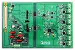
Figure 8 shows a photo of the EVAL-CN0364-SDPZ evaluation
board.
Mark Cantrell, Recommendations for Control of Radiated
Emissions with isoPower Devices, Application Note AN-0971,
Analog Devices.
HART® Communication Foundation
Data Sheets and Evaluation Boards
AD7173-8 Data Sheet
AD5700-1 Data Sheet
ADuM3151 Data Sheet
ADuM5211 Data Sheet
ADG704 Data Sheet
12592-008
ADP2441 Data Sheet
Figure 8. Photo of EVAL-CN0364-SDPZ Evaluation Board
REVISION HISTORY
12/14—Revision 0: Initial Version
(Continued from first page) Circuits from the Lab reference designs are intended only for use with Analog Devices products and are the intellectual property of Analog Devices or its licensors.
While you may use the Circuits from the Lab reference designs in the design of your product, no other license is granted by implication or otherwise under any patents or other intellectual
property by application or use of the Circuits from the Lab reference designs. Information furnished by Analog Devices is believed to be accurate and reliable. However, Circuits from the
Lab reference designs are supplied "as is" and without warranties of any kind, express, implied, or statutory including, but not limited to, any implied warranty of merchantability,
noninfringement or fitness for a particular purpose and no responsibility is assumed by Analog Devices for their use, nor for any infringements of patents or other rights of third parties
that may result from their use. Analog Devices reserves the right to change any Circuits from the Lab reference designs at any time without notice but is under no obligation to do so.
©2014 Analog Devices, Inc. All rights reserved. Trademarks and
registered trademarks are the property of their respective owners.
CN12592-0-12/14(0)
Rev. 0 | Page 6 of 6
�