Circuit Note
CN-0509
Devices Connected/Referenced
Circuits from the Lab® reference designs are engineered and
tested for quick and easy system integration to help solve today’s
analog, mixed-signal, and RF design challenges. For more
information and/or support, visit www.analog.com/CN0509.
LTC7103
105 V, 2.3 A Low EMI Synchronous StepDown Regulator
LT8302
42 VIN Micropower No Opto Isolated
Flyback Converter with 65 V/3.6 A Switch
Wide Input Voltage Range, Dual USB Port Charger
EVALUATION AND DESIGN SUPPORT
supplies, random stacks of alkaline battery cells, motors hacked
to run as generators, and wind turbines. The CN-0509 includes
two USB charging ports that can provide 2 A at 5 V. One port
includes a dedicated charging port (DCP) controller that enables
the fast charging modes for devices from most manufacturers.
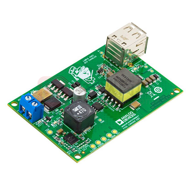
Circuit Evaluation Boards
CN-0509 Circuit Evaluation Board (EVAL-CN0509-EBZ)
Design and Integration Files
Schematics, Layout Files, Bill of Materials
CIRCUIT FUNCTION AND BENEFITS
Finding a power source to charge cell phones or other USB
communication devices can be difficult during emergency
situations, such as natural disasters or extended power outages.
Chargers operating from ac mains are ubiquitous, but when a
power grid is unavailable, and the last USB battery backup charger
systems are depleted, how else can critical USB powered devices
be charged?
The circuit shown in Figure 1 is a wide input voltage range USB
device charger capable of providing 2 A at 5 V for a wide range of
dc power sources, including solar panels, fully charged or half
discharged car batteries, −48 V telecommunications backup
This circuit accepts any dc voltage from 5 V to 100 V and
produces an isolated 5 V supply via a standard USB, Type A
connector. Isolation prevents faults in situations in which the
relationship of the power source to Earth ground is unknown
because the outer case of many cell phones and other portable
electronics are often electrically connected to USB ground.
The circuit shown in Figure 1 is also protected from reverse
voltage conditions. Because the polarity of a makeshift power
supply may not be known, the circuit can survive reverse
connection to the dc power source. This design contains light
emitting diodes (LEDs) that indicate whether the voltage source
is connected properly or must be swapped.
INPUT POLARITY INDICATOR
GREEN LED
DRIVER
(TRANSISTOR)
RED LED
DRIVER
(TRANSISTOR)
USB2
LTC7103
(BUCK REGULATOR)
2.5A
FUSE
LTC8302
SW
FLYBACK
RFB
CONVERTER
USB CHARGE DM1
PORT
CONTROLLER DP1
USB1
20199-001
VIN
Figure 1. CN0509 Wide Range Isolated Device Charger Simplified Schematic
Rev. 0
Circuits from the Lab® reference designs from Analog Devices have been designed and built by Analog
Devices engineers. Standard engineering practices have been employed in the design and
construction of each circuit, and their function and performance have been tested and verified in a lab
environment at room temperature. However, you are solely responsible for testing the circuit and
determining its suitability and applicability for your use and application. Accordingly, in no event shall
Analog Devices be liable for direct, indirect, special, incidental, consequential or punitive damages due
toanycausewhatsoeverconnectedtotheuseofanyCircuitsfromtheLabcircuits. (Continuedonlastpage)
One Technology Way, P.O. Box 9106, Norwood, MA 02062-9106, U.S.A.
Tel: 781.329.4700
www.analog.com
Fax: 781.461.3113
©2020 Analog Devices, Inc. All rights reserved.
�CN-0509
Circuit Note
CIRCUIT DESCRIPTION
R1
270kΩ
The CN-0509 converts a wide array of dc power sources from
5 V to 100 V into a regulated 5 V, 2 A supply capable of charging
USB charged devices through a dual USB, Type A receptacle.
This design uses a combination of a high efficiency, step-down
(buck) dc to dc converter (LTC7103), capable of passthrough
operation, and an isolated flyback converter (LT8302). This
configuration combines the high power efficiency and wide
operating range of a buck converter with the isolation and
excellent regulation of a flyback converter.
Input Voltage Protection and LED Driver
The CN-0509 power entry stage is shown in Figure 2. A high
voltage Schottky diode and fuse protect the circuit from reverse
supply connection and overcurrent conditions.
INPUT POLARITY INDICATOR
B
DZTA42-13
3E
DSS120UTR
DSS120UTR
DS2
REVERSED
DS1
CORRECT
Q1
Q2
SML-P11MTT86R
SML-P11VTT86
MBT3904DW1T1G
MBT3904DW1T1G
R4
240Ω
R2
240Ω
GND
VIN
Figure 3. Polarity Indication
When power is applied, current flows through R1, which turns
on Transistor Q3. Current then flows through the emitter of Q3,
the LED, and R2. As the current increases through R2, the voltage
across R2 increases as well. Once the voltage drop across R2 reaches
the base to emitter voltage (VBE) of transistor Q1 (approximately
0.7 V), Q1 begins to turn on. The resulting current through R1
reduces the base drive to Q1, effectively limiting current to the
LED. This feedback loop maintains the green LED and the red
LED current at approximately 2.41 mA and 2.432 mA, respectively,
over a voltage range of 11 V to 100 V.
The power entry circuit is followed by an LTC7103 synchronous
buck converter. A buck converter, or step-down switch mode
power supply, efficiently reduces a higher dc voltage to a lower
voltage with low power dissipation and high power density in
a small package relative to a linear regulator of similar current
capability.
20199-002
LTC7103
VIN
D6
3E
LTC7103 Buck Converter
RED LED
DRIVER
(TRANSISTOR)
2.5A
FUSE
D2
Q4
4 2
C
1
Figure 2. Input Voltage Protection Circuit
Two LEDs indicate the input power, green indicates correct
polarity and red indicates a reversed connection. If the red LED
appears, the input connections must be reversed for the circuit
to operate. While a bridge rectifier could be used to allow operation
in either polarity, the additional 400 mV drop increases the
minimum operating voltage, which can be an issue when charging
from lower voltage sources, such as solar panels or alkaline
battery cells.
The dc input is filtered and bypassed by a total of 4.8 µF before
going into the input of the buck converter. The LTC7103 then
efficiently steps down the wide input voltage range of 12 V to
105 V to a regulated output voltage (VOUT) of 12 V while
delivering up to 2.3 A of output current at a 300 kHz switching
frequency (fSW).
An active, constant current driver circuit maintains LED
current over the entire operating range of the circuit, with
minimal variation in brightness. Two circuits are connected
in series, however, with opposite polarity (see Figure 3).
100
95
90
85
80
75
70
65
fSW = 300kHz
VIN = 100V
VIN = 72V
VIN = 48V
VIN = 24V
60
55
50
0.1
1
10
100
LOAD CURRENT (mA)
1000
20199-004
VIN
DZTA42-13
B
EFFICIENCY (%)
GREEN LED
DRIVER
(TRANSISTOR)
R3
270kΩ
20199-003
Two output ports are provided, one that leaves the USB D+
and D− signals open for general-purpose charging and one that
includes a USB DCP controller that enables the high current
charging modes for devices from most manufacturers. Both ports
can be used simultaneously. However, the maximum total load
current is 2 A.
Q3
4 2
C
1
Figure 4. Efficiency at 12 V VOUT and Various Input Voltage Conditions
Rev. 0 | Page 2 of 7
�Circuit Note
CN-0509
The LTC7103 includes a selectable precision internal feedback
divider, eliminating the need for external precision resistors.
The digital state of the VPRG1 and VPRG2 pins sets the output
voltage to one of the nine fixed options between 1.0 V and 15 V.
Note that the CN-0509 sets the output to 12 V by tying the
VPRG1 pin to the INTVCC pin and leaving the VPRG2 pin open.
5
VPRG1 = GND
VPRG2 = OPEN
OUTPUT VOLTAGE (V)
4
The CN-0509 takes advantage of the ability of the LTC7103 to
operate in passthrough mode when the input voltage is between
4.4 V and 12 V (see Figure 5). The isolated flyback stage following
the LTC7103 is optimized for 12 V but continues to operate
down to voltages as low as 5 V with a reduced output current
capability. Passthrough operation allows the circuit to continue to
operate as long as possible, even as the voltages of the emergency
power source begins to drop.
2
0
1
0
2
3
LOAD CURRENT (A)
20199-006
1
Figure 6. Typical LTC7103 Current-Limit Operation
13
LT8302 Flyback Converter
12
The buck stage is followed by an LT8302 micropower, no opto,
isolated flyback converter. The LT8302 maintains regulation by
indirectly sensing the output voltage by sampling the primary
side flyback waveform, eliminating the need for optocouplers or
a third sense winding on the coupled inductor.
11
10
9
8
Isolation is essential in this application because the polarity and
ground connections of a makeshift power source may not be
known or may inherently be incorrect for a charging application
by design. A −48 V telecommunications supply is a common
example (see Figure 7).
7
6
4
0
10
20
30
40
50
60
70
80
90
INPUT VOLTAGE (V)
100
20199-005
5
TELECOM
SUPPLY
Figure 5. Passthrough Operation for 4.4 V < VIN < 12 V
NONISOLATED
BUCK SUPPLY
VIN
The architecture of the LTC7103 provides inherent protection
against short-circuit conditions without the need for folding
back the output current or the oscillator frequency. This
protection is made possible because the pulse-width modulation
(PWM) comparator is continuously receiving inductor current
information from the average current amplifier. This results in
automatic cycle skipping under short-circuit conditions if the
minimum on time of the top switch is too long to maintain
control of the inductor current at the full switching frequency.
Typical current-limit operation is shown in Figure 6.
5V
SW
CASE AT
–48V
GND
+
48V
USB
CELLPHONE
–
–48V
HAZARD!
EARTH
Figure 7. Ground Fault Condition
Telecommunication supplies are negative with respect to Earth
ground to prevent galvanic corrosion of wires. Therefore, a
charger based on a nonisolated buck converter ties the outer
case of a cell phone to −48 V, posing a hazard if the case comes
into contact with a grounded object. Similar situations can
occur with improperly wired solar panels or generators.
Rev. 0 | Page 3 of 7
20199-007
OUTPUT VOLTAGE (V)
3
�Circuit Note
RREF × N PS × (VOUT + VF (T0))
VREF
Figure 8 shows the typical maximum output power at 5 V VOUT
for common winding ratio values at various input voltages. The
CN-0509 transformer has a 3:1 turns ratio for a maximum VOUT
of approximately 10 W.
20
OUTPUT POWER (W)
U3
5V, 2A
SUPPLY
where:
RFB is the LT8302 feedback resistor.
RREF is the LT8302 reference resistor.
NPS is the transformer effective primary to secondary turns ratio.
VOUT is the output voltage.
VF(T0) is the output diode forward voltage at 25°C = ~0.3 V.
VREF is the LT8302 internal voltage reference.
MAXIMUM OUTPUT POWER
N = 4:1
N = 3:1
N = 2:1
N = 1:1
15
GND
IN
DM
GND
VBUS
DP
D–
D+
GND
GND
20199-009
RFB =
VBUS
VBUS
USB CONNECTOR 2
(BOTTOM)
In addition to providing isolation, the LT8302 further steps
down the 12 V output from the buck converter to 5 V. VOUT is
programmed using two external resistors and a third optional
temperature compensation resistor as follows:
USB CONNECTOR 1
(TOP)
CN-0509
Figure 9. USB Dedicated Charging Port Controller
U3 is a DCP controller that monitors the USB data line voltages
(D+ and D−) and provides signatures for enabling fast charging
modes for several common device manufacturers (see Figure 9).
While both ports can be used simultaneously up to a maximum
total load current of 2 A, when using the DCP port, leaving the
other port disconnected is recommended.
Note that the quality of USB cables varies significantly. Long,
small gauge cables can result in significant voltage drop at the load.
System Performance
CN-0509 operation is nearly constant for any input voltage between
12 V and 100 V because the input to the isolated converter is at
a constant 12 V. Lower input voltage reduces the available
charging current according to Figure 10.
10
5
10
20
30
INPUT VOLTAGE (V)
40
Figure 8. Typical Maximum Output Power at 5 V VOUT
Fast Charging Up to 2 A
USBs have become a defacto standard for device charging, and
typical chargers can deliver more than the minimum 500 mA
USB 2.0 specification. Chargers must provide a special voltage
signature on USB data lines to let the device recognize itself and
to determine the maximum charging current it can draw from
the power source, which can be higher than the 500 mA
minimum standard.
Rev. 0 | Page 4 of 7
2.0
1.5
1.0
0.5
0
0
10
20
30
40
50
60
70
80
90
INPUT VOLTAGE (V)
Figure 10. Maximum Load Current vs. Input Voltage
100
20199-010
0
MAXIMUM LOAD CURRENT (A)
0
20199-008
2.5
�Circuit Note
CN-0509
Reverse Input Survival
Load Connection Transient
The CN-0509 is able to survive reverse input connections up to
100 V. Figure 11 shows the reverse input to the CN-0509 vs. the
LTC7103VIN.
Figure 13 and Figure 14 show the CN-0509 turn on transient
curves for the current and USB data lines for a cell phone
(Phone A) and USB power bank (Power Bank B), respectively.
20
LTC7103 V IN (mV)
15
10
1V/DIV
1V/DIV
5
0
500mA/DIV
C3
–10
0
–20
–40
–60
–80
–100
VIN (V)
20199-011
C2
20199-013
ILOAD
D–
D+
–5
TIME (1s/DIV)
Figure 13. ILOAD, D+, and D− Voltages of Phone A Charging
Figure 11. LTC7103 VIN vs. VIN
Load Regulation
Figure 12 shows that the load regulation of the CN-0509 across
input voltages above 12 V is within 65 mV because the load
increases from 0.1 A to 2 A, corresponding to an output
impedance of approximately 32.3 mΩ.
1V/DIV
1V/DIV
5.19
C3
5.18
50mV/DIV
5.17
5.15
TIME (1ms/DIV)
Figure 14. Bus Voltage (VBUS), D+, and D− Voltages of Power Bank B
5.14
5.13
5.12
5.11
5.10
0
0.5
1.0
1.5
ILOAD (A)
2.0
20199-012
VOUT (V)
5.16
20199-014
VBUS
D–
D+
C2
Figure 12. VOUT vs. Load Current (ILOAD)
Rev. 0 | Page 5 of 7
�CN-0509
Circuit Note
Test Setup and Functional Block Diagram
Figure 15 displays the thermal response of CN-0509 while
charging a load at 5.62 V, 2 A for one hour with the board
positioned horizontally above a workbench in still air at 25°C
ambient. The maximum temperature on the EVAL-CN0509EBZ board occurs on the D3 diode at 83.8°C, well below the
maximum operating temperature of 150°C.
A functional block diagram of the test setup is shown in Figure 16.
DC
SUPPLY
EVAL-CN0509-EBZ
USB
MULTIMETER
TESTER
WIRES/
WIRED OUT
USB CABLE
DEVICE/
LOAD
20199-016
Thermal Performance
Figure 16. Functional Block Diagram of the Test Setup
Setup and Test
Take the following steps for test setup:
1.
20199-015
2.
Figure 15. Thermal Image of EVAL-CN0509-EBZ at 5.62 V, 2 A Output
Charging a Load for One Hour
3.
4.
COMMON VARIATIONS
If mains supplies are available, the EVAL-CN0509-EBZ can turn
a wide variety of random offline power supplies into a USB charger.
Such supplies include laptop chargers, game console chargers,
and computer peripheral power supplies.
Using a Schottky bridge rectifier at power entry allows operation
regardless of input polarity. However, this input configuration
is at the expense of a 0.4 V increase in minimum operating
voltage over using a single protection diode. For example, a
VIN of 12.4 V is required for the full 2 A output current.
5.
6.
7.
Connect the input dc supply to P1 on the CN-0509. Use
caution when connecting high input voltages.
Upon turning on the dc input, the CN-0509 turns on. The
circuit determines if the input connection is in correct polarity
through lighting DS1 or DS2.
a. If DS1 (green LED) illuminates, the correct polarity is
on the input, and the circuit delivers up to 10 W on P2,
the USB output ports.
b. If DS2 (red LED) illuminates, turn off the input supply,
disconnect the power inputs, swap the power leads,
reconnect the supply outputs to P1, then repeat Step 2.
Connect the USB cable from the ET910 USB multimeter
tester to the lower USB port on the EVAL-CN0509-EBZ.
Connect a fast charge capable device from the ET910 USB
multimeter tester using the charging cable of the device.
Look at the ET910 USB multimeter tester and verify that
the device is pulling more than 500 mA but less than 2 A
(see Figure 17).
Swap the USB port on the EVAL-CN0509-EBZ from the
lower (DCP) port to the upper USB port.
Look at the ET910 USB multimeter tester and verify that the
device is pulling approximately 500 mA (see Figure 17).
CIRCUIT EVALUATION AND TEST
20199-017
For complete setup details and additional information on the
CN-0509, see the CN0509 User Guide.
Figure 17. ET910 USB Multimeter Tester Screenshot of Phone A Charging from the
Top USB Port (Left) vs. the Lower Port with the DCP Controller (Right)
Equipment Needed
The following equipment is needed :
•
•
•
•
•
A dc power supply (any voltage, 5 V to 100 V)
The EVAL-CN0509-EBZ evaluation board
A Klein Tools® ET910 USB multimeter tester (or equivalent)
A MicroUSB to USB Type A cable
A device with USB charging capability (cell phone, tablet,
or portable power pack) and a USB charging cable for the
device
Rev. 0 | Page 6 of 7
�Circuit Note
CN-0509
LEARN MORE
Data Sheets and Evaluation Boards
CN0509 Design Support Package:
https://www.analog.com/CN0509-DesignSupport
LTC7103 Data Sheet
CN0509 User Guide
DC2317A Demonstration Circuit
Triggs, Robert. (June 30, 2019). How fast charging really works.
Android Authority.
DC2014A Demonstration Circuit
Sengupta, Anirban. (January 14, 2016). Introduction to USB
Power Delivery. ElectronicDesign.
11/2020—Revision 0: Initial Version
LT8302 Data Sheet
REVISION HISTORY
(Continued from first page) Circuits from the Lab reference designs are intended only for use with Analog Devices products and are the intellectual property of Analog Devices or its licensors.
While you may use the Circuits from the Lab reference designs in the design of your product, no other license is granted by implication or otherwise under any patents or other intellectual
property by application or use of the Circuits from the Lab reference designs. Information furnished by Analog Devices is believed to be accurate and reliable. However, Circuits from the
Lab reference designs are supplied "as is" and without warranties of any kind, express, implied, or statutory including, but not limited to, any implied warranty of merchantability,
noninfringement or fitness for a particular purpose and no responsibility is assumed by Analog Devices for their use, nor for any infringements of patents or other rights of third parties
that may result from their use. Analog Devices reserves the right to change any Circuits from the Lab reference designs at any time without notice but is under no obligation to do so.
©2020 Analog Devices, Inc. All rights reserved. Trademarks and
registered trademarks are the property of their respective owners.
CN20199-11/20(0)
Rev. 0 | Page 7 of 7
�