FEATURES
FUNCTIONAL BLOCK DIAGRAM
Low insertion loss: 0.7 dB typical at 2.0 GHz
High input third-order intercept (IP3): >60 dBm typical
Single positive control: 0 V or 3 V
Small, surface-mount, 8-lead, 2 mm × 2 mm LFCSP package
HMC1055
NIC 1
8 RF2
GND 2
7 VCTL
GND 3
6 VDD
NIC 4
5 RF1
APPLICATIONS
PACKAGE
BASE
Cellular infrastructure
Wireless infrastructure
Mobile radios
Test equipment
GND
13718-001
Data Sheet
0.5 GHz to 4.0 GHz, GaAs, SPST Switch
HMC1055
Figure 1.
GENERAL DESCRIPTION
The HMC1055 is a low cost, gallium arsenide (GaAs), singlepole, single-throw (SPST) switch in a surface-mount LFCSP
package. This switch offers low insertion loss, high isolation,
and exceptional third-order intermodulation performance that
make it ideal for many cellular and wireless infrastructure
applications from 0.5 GHz to 4.0 GHz.
Rev. B
The HMC1055 operates with single positive supply voltage and
a single positive control voltage at very low dc currents. RF1 is
reflective open, whereas RF2 is terminated to 50 Ω in the off state.
Document Feedback
Information furnished by Analog Devices is believed to be accurate and reliable. However, no
responsibility is assumed by Analog Devices for its use, nor for any infringements of patents or other
rights of third parties that may result from its use. Specifications subject to change without notice. No
license is granted by implication or otherwise under any patent or patent rights of Analog Devices.
Trademarks and registered trademarks are the property of their respective owners.
One Technology Way, P.O. Box 9106, Norwood, MA 02062-9106, U.S.A.
Tel: 781.329.4700 ©2016–2018 Analog Devices, Inc. All rights reserved.
Technical Support
www.analog.com
�HMC1055
Data Sheet
TABLE OF CONTENTS
Features .............................................................................................. 1
Interface Schematics .....................................................................5
Applications ....................................................................................... 1
Typical Performance Characteristics ..............................................6
Functional Block Diagram .............................................................. 1
Theory of Operation .........................................................................8
General Description ......................................................................... 1
Applications Information .................................................................9
Revision History ............................................................................... 2
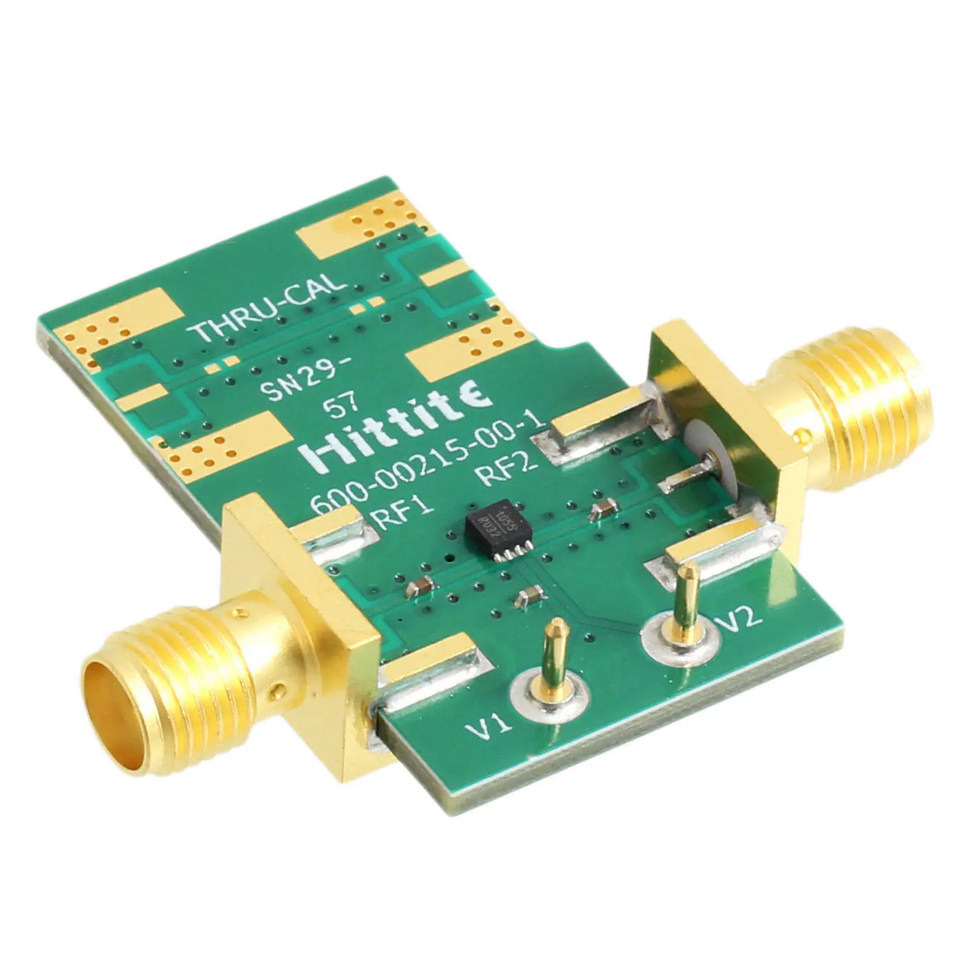
Evaluation Printed Circuit Board (PCB) ...................................9
Specifications..................................................................................... 3
Evaluation Board Schematic and Artwork ................................9
Absolute Maximum Ratings............................................................ 4
Outline Dimensions ....................................................................... 10
ESD Caution .................................................................................. 4
Ordering Guide .......................................................................... 10
Pin Configuration and Function Descriptions ............................. 5
REVISION HISTORY
8/2018—Rev. A to Rev. B
Changes to Reflow Temperature Parameter, Table 2 ................... 4
Updated Outline Dimensions ....................................................... 10
Changes to Ordering Guide .......................................................... 10
2/2016—v00.0912 to Rev. A
This Hittite Microwave Products data sheet has been reformatted
to meet the styles and standards of Analog Devices, Inc.
Changed NC to NIC ...................................................... Throughout
Changes to Title, Features Section, Applications Section,
Figure 1, and General Description Section ................................... 1
Changes to Table 1 ............................................................................ 3
Changes to Table 2 ............................................................................ 4
Added Figure 2; Renumbered Sequentially ...................................5
Changes to Table 3.............................................................................5
Deleted Typical Application Circuit ...............................................5
Changes to Figure 5 ...........................................................................6
Changes to Figure 11 and Figure 12................................................7
Changes to Theory of Operation Section and Table 4 .................8
Added Applications Information Section, Evaluation Printed
Circuit Board Section, Evaluation Board Schematic and
Artwork Section, and Figure 13; Renumbered Sequentially .......9
Changes to Table 5.............................................................................9
Updated Outline Dimensions ....................................................... 10
Changes to Ordering Guide .......................................................... 10
Rev. B | Page 2 of 10
�Data Sheet
HMC1055
SPECIFICATIONS
VDD = 3 V , VCTL = 0 V or VDD, TA = 25°C, 50 Ω system, unless otherwise noted.
Table 1.
Parameter
FREQUENCY
INSERTION LOSS
ISOLATION
RETURN LOSS
On State
Off State
INPUT LINEARITY
Input 0.1 dB Compression (P0.1dB)
Input Third-Order Intercept (IP3)
SWITCHING CHARACTERISTICS
Rise/Fall Time (tRISE, tFALL)
On/Off Time (tON, tOFF)
CURRENT
Supply (IDD)
Control (ICTL)
Test Conditions/Comments
0.5 GHz to 2.0 GHz
2.0 GHz to 4.0 GHz
0.5 GHz to 2.0 GHz
2.0 GHz to 4.0 GHz
0.7
1.4
36
28
Unit
GHz
dB
dB
dB
dB
0.5 GHz to 2.0 GHz, RF1 and RF2 ports
2.0 GHz to 4.0 GHz, RF1 and RF2 ports
0.5 GHz to 2.0 GHz, RF2 port
2.0 GHz to 4.0 GHz, RF2 port
0.5 GHz to 4.0 GHz
27
25
12
24
dB
dB
dB
dB
Two-tone input power = 15 dBm each tone
28
>60
dBm
dBm
10% to 90% RF
50% VCTL to 90% RF
40
50
ns
ns
VDD = 3 V to 5 V
0 V or VDD
0.2
很抱歉,暂时无法提供与“EVAL01-HMC1055LP2C”相匹配的价格&库存,您可以联系我们找货
免费人工找货