HMC-ALH444
v04.0417
AMPLIFIERS - LOW NOISE - CHIP
1
GaAs HEMT MMIC LOW NOISE
AMPLIFIER, 1 - 12 GHz
Typical Applications
Features
This HMC-ALH444 is ideal for:
Noise Figure: 1.75 dB @ 10 GHz
• Wideband Communication Systems
Gain: 17 dB
• Surveillance Systems
P1dB Output Power: +19 dBm @ 5 GHz
• Point-to-Point Radios
Supply Voltage: +5V @ 55 mA
• Point-to-Multi-Point Radios
Die Size: 2.64 x 1.64 x 0.1 mm
• Military & Space
• Test Instrumentation
* VSAT
General Description
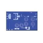
Functional Diagram
The HMC-ALH444 is a GaAs MMIC HEMT Low Noise
Wideband Amplifier die which operates between 1
and 12 GHz. The amplifier provides 17 dB of gain, 1.5
dB noise figure and +19 dBm of output power at 1 dB
gain compression while requiring only 55 mA from a
+5V supply voltage.
Electrical Specifications*, TA = +25° C, Vdd= +5V
Parameter
Min.
Frequency Range
Gain
Gain Variation over Temperature
Typ.
Max.
1 - 12
15
Units
GHz
17
dB
0.02
dB / °C
Noise Figure
1.5
2
dB
Input Return Loss
10
Output Return Loss
14
dB
Output IP3
28
dBm
Output Power for 1 dB Compression
19
dBm
Supply Current (Idd)
(Vdd = 5V, Vgg1 = -0.5V Typ., Vgg2 = 1.5V Typ)
55
mA
dB
*Unless otherwise indicated, all measurements are from probed die
1-1
Information
furnished
by Analog
is believed
to be
accurateDevices,
and reliable.
However,
For price,Way,
delivery,
placeNorwood,
orders: Analog
Devices, Inc.,
For price,
delivery,
andDevices
to place
orders:
Analog
Inc.,
OnenoTechnology
P.O.and
Boxto9106,
MA 02062-9106
responsibility is assumed by Analog Devices for its use, nor for any infringements of patents or other
One
Technology Way, P.O. Box 9106, Norwood, MA 02062-9106
Phone: 781-329-4700
• Order
at www.analog.com
rights of third parties that may result from its use. Specifications
subject to change without
notice.online
No
Phone:
781-329-4700
•
Order
online
at
www.analog.com
license is granted by implication or otherwise under any patent
or patent rights
of AnalogPhone:
Devices. 1-800-ANALOG-D
Application
Support:
Application Support: Phone: 1-800-ANALOG-D
Trademarks and registered trademarks are the property of their respective owners.
�HMC-ALH444
v04.0417
GaAs HEMT MMIC LOW NOISE
AMPLIFIER, 1 - 12 GHz
1
Noise Figure vs. Frequency
Linear Gain vs. Frequency
18
NOISE FIGURE (dB)
16
GAIN (dB)
14
12
10
8
6
4
2
1.5
1
0.5
2
0
0
0
2
4
6
8
10
12
0
14
2
4
6
8
10
12
14
FREQUENCY (GHz)
FREQUENCY (GHz)
Input Return Loss vs. Frequency
Output Return Loss vs. Frequency
0
0
RETURN LOSS (dB)
RETURN LOSS (dB)
-5
-5
-10
-15
-10
-15
-20
-25
-30
AMPLIFIERS - LOW NOISE - CHIP
2.5
20
-35
-20
-40
0
2
4
6
8
FREQUENCY (GHz)
10
12
14
0
2
4
6
8
10
12
14
FREQUENCY (GHz)
For price, delivery, and to place orders: Analog Devices, Inc., One Technology Way, P.O. Box 9106, Norwood, MA 02062-9106
Phone: 781-329-4700 • Order online at www.analog.com
Application Support: Phone: 1-800-ANALOG-D
1-2
�HMC-ALH444
v04.0417
AMPLIFIERS - LOW NOISE - CHIP
1
Absolute Maximum Ratings
Drain Bias Voltage
+5.5 Vdc
RF Input Power
12 dBm
Gate Bias Voltage Vgg1
-1 to 0.3 Vdc
Gate Bias Voltage Vgg2
0 to 2.5 Vdc
Thermal Resistance
(channel to die bottom)
109 °C/W
Channel Temperature
180 °C
Storage Temperature
-65 to +150 °C
Operating Temperature
-55 to +85 °C
ESD Rating
Class 0
ELECTROSTATIC SENSITIVE DEVICE
OBSERVE HANDLING PRECAUTIONS
Outline Drawing
Die Packaging Information [1]
Standard
Alternate
GP-1 (Gel Pack)
[2]
[1] Refer to the “Packaging Information” section for die
packaging dimensions.
[2] For alternate packaging information contact Hittite
Microwave Corporation.
1-3
GaAs HEMT MMIC LOW NOISE
AMPLIFIER, 1 - 12 GHz
NOTES:
1. ALL DIMENSIONS ARE IN INCHES [MM].
2. TYPICAL BOND PAD IS .004” SQUARE.
3. BACKSIDE METALLIZATION: GOLD.
4. BACKSIDE METAL IS GROUND.
5. BOND PAD METALLIZATION: GOLD.
6. CONNECTION NOT REQUIRED FOR UNLABELED BOND PADS.
7. OVERALL DIE SIZE ±.002”
For price, delivery, and to place orders: Analog Devices, Inc., One Technology Way, P.O. Box 9106, Norwood, MA 02062-9106
Phone: 781-329-4700 • Order online at www.analog.com
Application Support: Phone: 1-800-ANALOG-D
�HMC-ALH444
v04.0417
GaAs HEMT MMIC LOW NOISE
AMPLIFIER, 1 - 12 GHz
Pad Number
Function
Description
1
RFIN
This pad is AC coupled
and matched to 50 Ohms.
2
RFOUT
This pad is AC coupled
and matched to 50 Ohms.
3
Vdd
Power Supply Voltage for the amplifier. See assembly for
required external components.
4, 5
Vgg1, Vgg2
Gate control for amplifier. Please follow “MMIC Amplifier Biasing Procedure” application note. See assembly for required
external components.
Die bottom
GND
Die bottom must be connected to RF/DC ground.
Interface Schematic
For price, delivery, and to place orders: Analog Devices, Inc., One Technology Way, P.O. Box 9106, Norwood, MA 02062-9106
Phone: 781-329-4700 • Order online at www.analog.com
Application Support: Phone: 1-800-ANALOG-D
AMPLIFIERS - LOW NOISE - CHIP
1
Pad Descriptions
1-4
�HMC-ALH444
v04.0417
Assembly Diagram
AMPLIFIERS - LOW NOISE - CHIP
1
GaAs HEMT MMIC LOW NOISE
AMPLIFIER, 1 - 12 GHz
Note 1: Bypass caps should be 100 pF (approximately) ceramic (single-layer) placed no farther than 30 mils from the amplifier.
Note 2: Best performance obtained from use of