HMC-ALH482
v04.1009
LOW NOISE AMPLIFIERS - CHIP
1
GaAs HEMT MMIC LOW NOISE
AMPLIFIER, 2 - 22 GHz
Typical Applications
Features
This HMC-ALH482 is ideal for:
Noise Figure: 1.7 dB @ 2-12 GHz
• Wideband Communication Systems
Noise Figure: 2.2 dB @ 12-22 GHz
• Surveillance Systems
Gain: 16 dB @ 12 GHz
• Point-to-Point Radios
P1dB Output Power: +14 dBm
• Point-to-Multi-Point Radios
Supply Voltage: +4V @ 45 mA
• Military & Space
Die Size: 2.04 x 1.2 x 0.1 mm
• Test Instrumentation
General Description
Functional Diagram
The HMC-ALH482 is a GaAs MMIC HEMT Low Noise
Wideband Amplifier die which operates between 2
and 22 GHz. The amplifier provides 16 dB of gain, 1.7
dB noise figure up to 12 GHz and +14 dBm of output
power at 1 dB gain compression while requiring only
45 mA from a +4V supply voltage. The HMC-ALH482
amplifier is ideal for integration into Multi-ChipModules (MCMs) due to its small size.
Electrical Specifi cations*, TA = +25° C, Vdd= +4V
Parameter
Min.
Frequency Range
Gain
Typ.
Max.
Min.
2 - 12
15
Gain Variation over Temperature
Noise Figure
16
15
0.01
1.7
Typ.
Max.
12 - 22
2.5
Units
GHz
16
dB
0.01
dB / °C
2.2
3
dB
Input Return Loss
8
6
dB
Output Return Loss
10
5
dB
Output Power for 1 dB Compression
14
14
dBm
Supply Current (Idd) (Vdd = 4V, Vgg = -0.2V Typ.)
45
45
mA
*Unless otherwise indicated, all measurements are from probed die
1 - 204
For price,
delivery,
and to placeCorporation:
orders: Analog Devices, Inc.,
For price, delivery, and to place orders, please contact
Hittite
Microwave
One Technology Way, P.O. Box 9106, Norwood, MA 02062-9106
20 Alpha Road, Chelmsford, MA 01824 Phone:Phone:
978-250-3343
978-250-3373
781-329-4700Fax:
• Order
online at www.analog.com
Application Support: Phone: 1-800-ANALOG-D
Order On-line at www.hittite.com
Information furnished by Analog Devices is believed to be accurate and reliable. However, no
responsibility is assumed by Analog Devices for its use, nor for any infringements of patents or other
rights of third parties that may result from its use. Specifications subject to change without notice. No
license is granted by implication or otherwise under any patent or patent rights of Analog Devices.
Trademarks and registered trademarks are the property of their respective owners.
�HMC-ALH482
v04.1009
GaAs HEMT MMIC LOW NOISE
AMPLIFIER, 2 - 22 GHz
3
20
18
2.5
NOISE FIGURE (dB)
16
GAIN (dB)
14
12
10
8
6
4
2
1.5
1
0.5
2
0
0
0
2
4
6
8
10
12
14
16
18
20
22
0
24
2
4
6
FREQUENCY (GHz)
8
10
12
14
16
18
20
22
24
22
24
FREQUENCY (GHz)
Input Return Loss vs. Frequency
Output Return Loss vs. Frequency
0
0
-4
RETURN LOSS (dB)
RETURN LOSS (dB)
-2
-6
-8
-10
-12
-5
-10
-15
LOW NOISE AMPLIFIERS - CHIP
1
Noise Figure vs. Frequency
Linear Gain vs. Frequency
-20
-14
-16
-25
0
2
4
6
8
10
12
14
16
18
20
22
24
FREQUENCY (GHz)
0
2
4
6
8
10
12
14
16
18
20
FREQUENCY (GHz)
For price,
delivery,
and to placeCorporation:
orders: Analog Devices, Inc.,
For price, delivery, and to place orders, please contact
Hittite
Microwave
One Technology Way, P.O. Box 9106, Norwood, MA 02062-9106
20 Alpha Road, Chelmsford, MA 01824 Phone: Phone:
978-250-3343
978-250-3373
781-329-4700Fax:
• Order
online at www.analog.com
Application Support: Phone: 1-800-ANALOG-D
Order On-line at www.hittite.com
Information furnished by Analog Devices is believed to be accurate and reliable. However, no
responsibility is assumed by Analog Devices for its use, nor for any infringements of patents or other
rights of third parties that may result from its use. Specifications subject to change without notice. No
license is granted by implication or otherwise under any patent or patent rights of Analog Devices.
Trademarks and registered trademarks are the property of their respective owners.
1 - 205
�HMC-ALH482
v04.1009
GaAs HEMT MMIC LOW NOISE
AMPLIFIER, 2 - 22 GHz
LOW NOISE AMPLIFIERS - CHIP
1
Absolute Maximum Ratings
Drain Bias Voltage
+5 Vdc
Drain Bias Current
60 mA
RF Input Power
5 dBm
Gate Bias Voltage
-1 to 0.3 Vdc
Channel Temperature
180 °C
Continuous Pdiss (T = 85 °C)
derate 4.7 mW/ °C above 85 °C
0.45 W
Thermal Resistance
(channel to die bottom)
213.3 °C/W
Storage Temperature
-65 to +150 °C
Operating Temperature
-55 to +85 °C
Outline Drawing
Die Packaging Information [1]
Standard
Alternate
GP-2 (Gel Pack)
[2]
[1] Refer to the “Packaging Information” section for die
packaging dimensions.
[2] For alternate packaging information contact Hittite
Microwave Corporation.
1 - 206
ELECTROSTATIC SENSITIVE DEVICE
OBSERVE HANDLING PRECAUTIONS
NOTES:
1. ALL DIMENSIONS ARE IN INCHES [MM].
2. TYPICAL BOND PAD IS .004” SQUARE.
3. BACKSIDE METALLIZATION: GOLD.
4. BACKSIDE METAL IS GROUND.
5. BOND PAD METALLIZATION: GOLD.
6. CONNECTION NOT REQUIRED FOR UNLABELED BOND PADS.
7. OVERALL DIE SIZE ±.002”
For price,
delivery,
and to placeCorporation:
orders: Analog Devices, Inc.,
For price, delivery, and to place orders, please contact
Hittite
Microwave
One Technology Way, P.O. Box 9106, Norwood, MA 02062-9106
20 Alpha Road, Chelmsford, MA 01824 Phone:Phone:
978-250-3343
978-250-3373
781-329-4700Fax:
• Order
online at www.analog.com
Application Support: Phone: 1-800-ANALOG-D
Order On-line at www.hittite.com
Information furnished by Analog Devices is believed to be accurate and reliable. However, no
responsibility is assumed by Analog Devices for its use, nor for any infringements of patents or other
rights of third parties that may result from its use. Specifications subject to change without notice. No
license is granted by implication or otherwise under any patent or patent rights of Analog Devices.
Trademarks and registered trademarks are the property of their respective owners.
�HMC-ALH482
v04.1009
GaAs HEMT MMIC LOW NOISE
AMPLIFIER, 2 - 22 GHz
Pad Number
Function
Description
1
RFIN
This pad is AC coupled
and matched to 50 Ohms.
2
RFOUT
This pad is AC coupled
and matched to 50 Ohms.
3
Vdd
Power Supply Voltage for the amplifier. See assembly for
required external components.
4
Vgg
Gate control for amplifier. Please follow “MMIC Amplifier Biasing Procedure” application note. See assembly for required
external components.
Die bottom
GND
Die bottom must be connected to RF/DC ground.
Interface Schematic
For price,
delivery,
and to placeCorporation:
orders: Analog Devices, Inc.,
For price, delivery, and to place orders, please contact
Hittite
Microwave
One Technology Way, P.O. Box 9106, Norwood, MA 02062-9106
20 Alpha Road, Chelmsford, MA 01824 Phone: Phone:
978-250-3343
978-250-3373
781-329-4700Fax:
• Order
online at www.analog.com
Application Support: Phone: 1-800-ANALOG-D
Order On-line at www.hittite.com
Information furnished by Analog Devices is believed to be accurate and reliable. However, no
responsibility is assumed by Analog Devices for its use, nor for any infringements of patents or other
rights of third parties that may result from its use. Specifications subject to change without notice. No
license is granted by implication or otherwise under any patent or patent rights of Analog Devices.
Trademarks and registered trademarks are the property of their respective owners.
LOW NOISE AMPLIFIERS - CHIP
1
Pad Descriptions
1 - 207
�HMC-ALH482
v04.1009
GaAs HEMT MMIC LOW NOISE
AMPLIFIER, 2 - 22 GHz
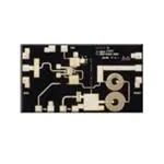
Assembly Diagram
LOW NOISE AMPLIFIERS - CHIP
1
Note 1: Bypass caps should be 100 pF (approximately) ceramic (single-layer) placed no farther than 30 mils from the amplifier.
Note 2: Best performance obtained from use of