0.1 GHz to 40 GHz, SPST Switch
HMC-C583
Data Sheet
FUNCTIONAL BLOCK DIAGRAM
7 dB typical insertion loss
Single positive control line
50 dB typical isolation
Input third-order intercept (IP3): 40 dBm
CMOS-compatible control
Nonreflective topology
Hermetically sealed module
Field replaceable K-type connectors
Operating temperature: −55°C to +85°C
RF1
1
VDD
VCTL
GND
2
3
4
50Ω
50Ω
HMC-C583
RF2
5
12965-001
FEATURES
Figure 1.
APPLICATIONS
Base station infrastructure
Fiber optics and broadband telecommunications
Microwave radios and VSATs
Military radios, radars, and electronic counter measures (ECM)
Test instrumentation
GENERAL DESCRIPTION
The HMC-C583 is a 0.1 GHz to 40 GHz, gallium arsenide (GaAs),
pseudomorphic high electron mobility transfer (pHEMT), IC
single-pole, single-throw (SPST) switch housed in a miniature
hermetic module. This wideband switch features 7 dB typical
insertion loss, 50 dB typical isolation, and 40 dBm input IP3.
Rev. 0
The switching on/off time is 10 ns typical. A single control
voltage input, toggled between 0 V and 5 V, selects the switch
state. Removable K-type connectors can be detached to allow
direct connection of the input/output pins of the module to a
microstrip or coplanar circuit.
Document Feedback
Information furnished by Analog Devices is believed to be accurate and reliable. However, no
responsibility is assumed by Analog Devices for its use, nor for any infringements of patents or other
rights of third parties that may result from its use. Specifications subject to change without notice. No
license is granted by implication or otherwise under any patent or patent rights of Analog Devices.
Trademarks and registered trademarks are the property of their respective owners.
One Technology Way, P.O. Box 9106, Norwood, MA 02062-9106, U.S.A.
Tel: 781.329.4700
©2016 Analog Devices, Inc. All rights reserved.
Technical Support
www.analog.com
�HMC-C583
Data Sheet
TABLE OF CONTENTS
Features .............................................................................................. 1
Pin Configuration and Function Descriptions..............................5
Applications ....................................................................................... 1
Interface Schematics .....................................................................5
Functional Block Diagram .............................................................. 1
Typical Performance Characteristics ..............................................6
General Description ......................................................................... 1
Theory of Operation .........................................................................7
Revision History ............................................................................... 2
Applications Information .................................................................8
Specifications..................................................................................... 3
Outline Dimensions ..........................................................................9
Absolute Maximum Ratings............................................................ 4
Ordering Guide .............................................................................9
ESD Caution .................................................................................. 4
REVISION HISTORY
9/2016—Revision 0: Initial Version
Rev. 0 | Page 2 of 9
�Data Sheet
HMC-C583
SPECIFICATIONS
VDD = 5 V, VCTL = 0 V or 5 V, TA = 25°C, unless otherwise noted.
Table 1.
Parameter
INSERTION LOSS
ISOLATION
Symbol
INPUT POWER FOR 0.1 dB COMPRESSION
P0.1dB
INPUT THIRD-ORDER INTERCEPT
RETURN LOSS
SUPPLY INPUT
CONTROL INPUTS
Input Voltage
High
Low
Input Current
SWITCHING CHARACTERISTICS
Rise Time/Fall Time
On Time/Off Time
Min
Typ
7
Max
10
Unit
dB
40
50
dB
Test Conditions/Comments
0.1 GHz to 40 GHz
Includes insertion loss
0.1 GHz to 40 GHz
5
21
dBm
dBm
0.1 GHz to 0.5 GHz
0.5 GHz to 40 GHz
20
40
10
5
dBm
dBm
dB
V
0.1 GHz to 2 GHz
2 GHz to 40 GHz
0.1 GHz to 40 GHz
IP3
VDD
4.5
5.5
VINH
VINL
IIN
3.5 to VDD
0 to 1.5
±20
V
V
μA
VIN = 0 V or VDD
tRISE/tFALL
tON/tOFF
1
10
ns
ns
10%/90% radio frequency (RF)
50% VCTL to 10%/90% RF
Rev. 0 | Page 3 of 9
�HMC-C583
Data Sheet
ABSOLUTE MAXIMUM RATINGS
Stresses at or above those listed under Absolute Maximum
Ratings may cause permanent damage to the product. This is a
stress rating only; functional operation of the product at these
or any other conditions above those indicated in the operational
section of this specification is not implied. Operation beyond
the maximum operating conditions for extended periods may
affect product reliability.
Table 2.
Parameter
Supply Input (VDD)
Control Voltage (VCTL)
RF Input Power
0.1 GHz to 0.5 GHz
0.5 GHz to 2 GHz
2 GHz to 40 GHz
Hot Switch Power Level
0.1 GHz to 0.5 GHz
0.5 GHz to 2 GHz
2 GHz to 40 GHz
Operating Temperature Range
Storage Temperature Range
ESD Rating, Human Body Model (HBM)
Rating
5.8 V
VDD ± 0.5 V
5 dBm
18 dBm
25 dBm
3 dBm
16 dBm
23 dBm
−55°C to +85°C
−65°C to +150°C
Class 1A (>250 V)
ESD CAUTION
Rev. 0 | Page 4 of 9
�Data Sheet
HMC-C583
PIN CONFIGURATION AND FUNCTION DESCRIPTIONS
HMC-C583
5 RF2
2
3
4
VDD
VCTL
GND
TOP VIEW
12965-002
RF1 1
Figure 2. Pin Configuration
Table 3. Pin Function Descriptions
Pin No.
1
Mnemonic
RF1
2
3
4
5
VDD
VCTL
GND
RF2
Description
RF Input/Output 1. This pin is dc-coupled and matched to 50 Ω. Blocking capacitors are required if the RF line
potential is not equal to 0 V dc.
Positive Supply Voltage, 5 V DC.
Control Pin.
Power Supply Ground.
RF Input/Output 2. This pin is dc-coupled and matched to 50 Ω. Blocking capacitors are required if the RF line
potential is not equal to 0 V dc.
INTERFACE SCHEMATICS
12965-003
RF1/RF2
VCTL
Figure 3. RF1/RF2 Interface Schematic
–5V
INTERNAL
12965-004
GND
4.7kΩ
Figure 4. GND Interface Schematic
Figure 5. VCTL Interface Schematic
Rev. 0 | Page 5 of 9
12965-005
5V
ZENER
DIODE
�HMC-C583
Data Sheet
TYPICAL PERFORMANCE CHARACTERISTICS
0
0
–5
–10
RETURN LOSS (dB)
–4
–6
–55°C
+25°C
+85°C
–8
–15
–20
–25
–55°C
+25°C
+85°C
–30
–35
–40
12965-006
–10
–12
0
5
10
15
20
25
30
35
40
45
12965-009
INSERTION LOSS (dB)
–2
–45
–50
50
0
5
10
15
20
FREQUENCY (GHz)
25
30
35
40
45
50
FREQUENCY (GHz)
Figure 9. Return Loss vs. Frequency at Various Temperatures for RF1, RF2
Figure 6. Insertion Loss vs. Frequency at Various Temperatures
50
0
–10
40
–20
–55°C
+25°C
+85°C
–40
IP3 (dBm)
ISOLATION (dB)
–30
–50
–60
–55°C
+25°C
+85°C
30
20
–70
12965-007
–90
0
0
0
2
4
6
8
10
12
14
16
18
20
22
24
26
28
30
32
34
36
38
40
42
44
46
48
50
–100
12965-010
10
–80
5
10
FREQUENCY (GHz)
15
20
25
FREQUENCY (GHz)
30
35
40
Figure 10. IP3 vs. Frequency at Various Temperatures
Figure 7. Isolation vs. Frequency at Various Temperatures
20
30
18
–55°C
+25°C
+85°C
16
14
POWER (dBm)
20
–55°C
+25°C
+85°C
15
10
12
10
8
6
4
0
0
5
10
15
20
25
30
35
12965-011
5
2
12965-008
INPUT POWER (dBm)
25
0
0
40
0.2
0.4
0.6
0.8
1.0
FREQUENCY (GHz)
FREQUENCY (GHz)
Figure 8. Input 0.1 dB Compression (Low Frequency)
Figure 11. Input 0.1 dB Compression (High Frequency)
Rev. 0 | Page 6 of 9
1.2
�Data Sheet
HMC-C583
THEORY OF OPERATION
Applying a TTL-level voltage to the VCTL pin provides an
insertion loss between the RF1 and RF2 connectors from 7 dB
typical to 10 dB typical. When the HMC-C583 is in a high
insertion loss state, both the RF1 and RF2 pins are internally
terminated to 50 Ω.
Table 4.
VCTL Level
Low
High
The low state level is a voltage between 0 V and 1.5 V, and the
high state level is a voltage between 3.5 V and VDD.
Rev. 0 | Page 7 of 9
Typical Insertion Loss Level (dB)
7
50
�HMC-C583
Data Sheet
APPLICATIONS INFORMATION
This type of circuit can create modulated RF signals for various
applications, which is only one of the many applications of the
HMC-C583.
In Figure 12, the HMC-C583 makes an RF pulse modulator. In
this application circuit, the HMC-C583 modulates the amplitude of
the output of the synthesized RF signal generator.
RF PULSE MODULATOR
RF1
1
VCTL
GND
2
3
4
50Ω
50Ω
RF2
5
RF OUTPUT
HMC-C583
12965-012
HMC-T2240
SIGNAL
GENERATOR
VDD
Figure 12. Typical Application Circuit
Rev. 0 | Page 8 of 9
�Data Sheet
HMC-C583
OUTLINE DIMENSIONS
0.373
(9.46)
1.000
(25.40)
0.360 (9.15)
0.245 (6.21)
0.180
(4.57)
0.255
(6.48)
0.075
(1.91)
BOTTOM VIEW
0.160
(4.06)
0.772
(19.61)
1
5
0.900
(22.86)
0.475
(12.07)
2
0.064
(1.63)
3
4
TOP VIEW
0.105
(2.67)
Ø 0.098
(2.93)
END VIEW
0.030
(0.76)
END VIEW
0.105
(2.67)
0.03 × 45°
0.245
(6.22)
(SHOWN WITH MOUNTING SPACER REMOVED)
CHAMFER INDICATES
ORIENTATION
0.500
(12.70)
0.755
(19.18)
1.756 (44.60)
SIDE VIEW
SIDE VIEW
Ø 0.012
(0.305)
(SHOWN WITH MOUNTING SPACER REMOVED)
09-28-2015-A
0.056
(1.42)
PKG-000000
CONTROLLING DIMENSIONS ARE IN INCHES; MILLIMETER DIMENSIONS
(IN PARENTHESES) ARE ROUNDED-OFF INCH EQUIVALENTS FOR
REFERENCE ONLY AND ARE NOT APPROPRIATE FOR USE IN DESIGN.
Figure 13. 5-Lead Module with Connector Interface [MODULE]
(ML-5-1)
Dimensions shown in inches and (millimeters)
ORDERING GUIDE
Model1
HMC-C583
1
Temperature Range
–55°C to +85°C
Package Description
5-Lead Module with Connector Interface [MODULE]
This is an RoHS compliant part.
©2016 Analog Devices, Inc. All rights reserved. Trademarks and
registered trademarks are the property of their respective owners.
D12965-0-9/16(0)
Rev. 0 | Page 9 of 9
Package Option
ML-5-1
�
很抱歉,暂时无法提供与“HMC-C583”相匹配的价格&库存,您可以联系我们找货
免费人工找货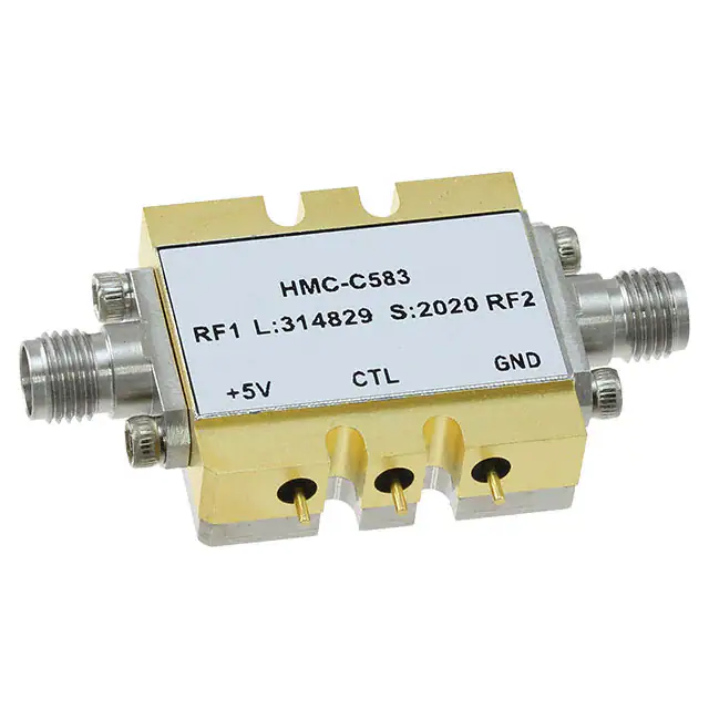


 工商网监
湘ICP备2023018690号
工商网监
湘ICP备2023018690号
