0.1 GHz to 40 GHz, 31 dB,
5-Bit Digital Attenuator
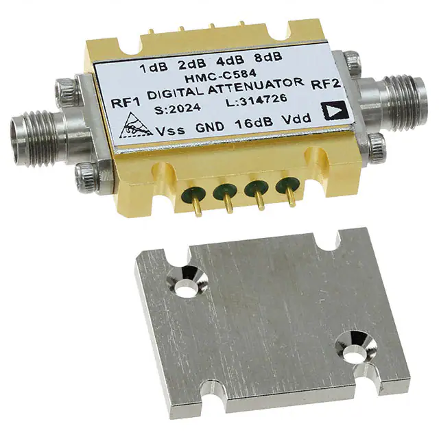
HMC-C584
Data Sheet
FEATURES
GENERAL DESCRIPTION
1.0 dB LSB steps to 31 dB
Single positive control line per bit
±1.0 dB typical bit error
Input IP3: 43 dBm
CMOS-compatible control
Hermetically sealed module
Field replaceable K-type connectors
Operating temperature: −55°C to +85°C
The HMC-C584 is a 0.1 GHz to 40 GHz, 5-bit, gallium arsenide
(GaAs) IC digital attenuator housed in a miniature hermetic
module. This wideband attenuator features 7 dB typical insertion
loss, 43 dBm input IP3, and bit values of 1 dB (LSB), 2 dB, 4 dB,
8 dB, and 16 dB for a total attenuation range of 31 dB. The
attenuation accuracy of the device has a ±1.0 dB typical step error.
Five control voltage inputs, toggled between 0 V and 5 V, are used
to select each attenuation state. Removable K-type connectors
can be detached to allow direct connection of the input/output
pins of the module to a microstrip or coplanar circuit.
APPLICATIONS
Fiber optics and broadband telecommunications
Microwave radios and VSATs
Military radios, radars, and electronic counter measures (ECM)
Space systems
Test instrumentation
FUNCTIONAL BLOCK DIAGRAM
10
9
8
7
V1
V2
V3
V4
16dB
8dB
4dB
2dB
1dB
HMC-C584
RF1
RF2
VSS
GND
V5
VDD
2
3
4
5
12966-001
6
1
Figure 1.
Rev. 0
Document Feedback
Information furnished by Analog Devices is believed to be accurate and reliable. However, no
responsibility is assumed by Analog Devices for its use, nor for any infringements of patents or other
rights of third parties that may result from its use. Specifications subject to change without notice. No
license is granted by implication or otherwise under any patent or patent rights of Analog Devices.
Trademarks and registered trademarks are the property of their respective owners.
One Technology Way, P.O. Box 9106, Norwood, MA 02062-9106, U.S.A.
Tel: 781.329.4700
©2016 Analog Devices, Inc. All rights reserved.
Technical Support
www.analog.com
�HMC-C584
Data Sheet
TABLE OF CONTENTS
Features .............................................................................................. 1
Pin Configuration and Function Descriptions..............................5
Applications ....................................................................................... 1
Typical Performance Characteristics ..............................................6
General Description ......................................................................... 1
Theory of Operation .........................................................................7
Functional Block Diagram .............................................................. 1
Applications Information .................................................................8
Revision History ............................................................................... 2
Outline Dimensions ..........................................................................9
Specifications..................................................................................... 3
Ordering Guide .............................................................................9
Absolute Maximum Ratings............................................................ 4
ESD Caution .................................................................................. 4
REVISION HISTORY
9/2016—Revision 0: Initial Version
Rev. 0 | Page 2 of 9
�Data Sheet
HMC-C584
SPECIFICATIONS
VDD = 5 V, VSS = −5 V, VCTL = 0 V/5 V, TA = 25°C, unless otherwise noted.
Table 1.
Parameter
INSERTION LOSS
0.1 GHz to 30 GHz
30 GHz to 40 GHz
ATTENUATION RANGE
0.1 GHz to 40 GHz
ATTENUATION ACCURACY
0.1 GHz to 30 GHz
1 dB to 8 dB States
Min
Typ
Max
Unit
4
7
8
9.5
10.5
dB
dB
24
31
35
dB
Normalized to insertion loss
16 dB to 31 dB States
30 GHz to 40 GHz
1 dB to 8 dB States
16 dB to 31 dB States
INPUT POWER FOR 0.1 dB COMPRESSION
0.1 GHz to 0.5 GHz
0.5 GHz to 40 GHz
INPUT IP3
0.1 GHz to 0.5 GHz
0.5 GHz to 40 GHz
RETURN LOSS
0.1 GHz to 40 GHz
SUPPLY INPUTS
VDD
VSS
CONTROL INPUTS
Input Voltage
High (VINH)
Low (VINL)
Input Current (IIN)
SWITCHING CHARACTERISTICS
Rise Time (tRISE)/Fall Time (tFALL)
On Time (tON)/Off Time (tOFF)
Test Conditions/Comments
±0.5 + 5% of maximum
attenuation setting
±0.6 + 6% of maximum
attenuation setting
dB
±0.8 + 8% of maximum
attenuation setting
±1.0 + 10% of maximum
attenuation setting
dB
20
25
dB
dB
40
43
dB
dB
10
dB
dB
dB
RF1 and RF2
4.5
−5.5
5
−5
5.5
−4.5
V
V
3.5 to 5
0 to 1.5
±5
V
V
μA
VIN = 0 V or VCC
60
90
ns
ns
10%/90 % RF
50% CTL to 10%/90 % RF
Rev. 0 | Page 3 of 9
�HMC-C584
Data Sheet
ABSOLUTE MAXIMUM RATINGS
Table 2.
Parameter
VDD
VSS
Control Voltage (V1 to V5)
RF Input Power
Operating Temperature Range
Storage Temperature Range
ESD Rating (HBM)
Rating
7V
−7 V
VDD + 0.5 V
25 dBm
−55°C to +85°C
−65°C to +150°C
Class 1A (>250 V)
Stresses at or above those listed under Absolute Maximum
Ratings may cause permanent damage to the product. This is a
stress rating only; functional operation of the product at these
or any other conditions above those indicated in the operational
section of this specification is not implied. Operation beyond
the maximum operating conditions for extended periods may
affect product reliability.
ESD CAUTION
Rev. 0 | Page 4 of 9
�Data Sheet
HMC-C584
PIN CONFIGURATION AND FUNCTION DESCRIPTIONS
10
V1
9
8
7
V2
V3
V4
HMC-C584
TOP VIEW
(Not to Scale)
RF1
RF2
VSS
GND
V5
VDD
2
3
4
5
6
12966-002
1
Figure 2. Pin Configuration
Table 3. Pin Function Descriptions
Pin No.
1
Mnemonic
RF1
2
3
4
5
6
VSS
GND
V5
VDD
RF2
7
8
9
10
V4
V3
V2
V1
Description
RF Input/Output 1. This pin is dc-coupled and matched to 50 Ω. Blocking capacitors are required if the RF
line potential is not equal to 0 V dc.
Negative Supply Voltage, 5 V DC.
Power Supply Ground.
Control Pin for the 16 dB Attenuation State.
Positive Supply Voltage, 5 V DC.
RF Input/Output 2. This pin is dc-coupled and matched to 50 Ω. Blocking capacitors are required if the RF
line potential is not equal to 0 V dc.
Control Pin for the 8 dB Attenuation State.
Control Pin for the 4 dB Attenuation State.
Control Pin for the 2 dB Attenuation State.
Control Pin for the 1 dB Attenuation State.
Rev. 0 | Page 5 of 9
�HMC-C584
Data Sheet
TYPICAL PERFORMANCE CHARACTERISTICS
0
0
–1
–10
RETURN LOSS (dB)
LEVEL (dB)
–3
–4
–5
–6
–7
–8
–20
0dB, S11 (dB)
0dB, S22 (dB)
1dB, S11 (dB)
1dB, S22 (dB)
2dB, S11 (dB)
2dB, S22 (dB)
4dB, S11 (dB)
4dB, S22 (dB)
8dB, S11 (dB)
8dB, S22 (dB)
16dB, S11 (dB)
16dB, S22 (dB)
31dB, S11 (dB)
31dB, S22 (dB)
–30
–40
–50
–9
0
5
10
15
20
25
FREQUENCY (GHz)
30
35
40
–60
12966-003
–10
0
5
10
15
20
25
FREQUENCY (GHz)
30
35
40
12966-006
–2
Figure 6. Return Loss for RF1, RF2
Figure 3. Insertion Loss
1.5
0
1.0
–5
–15
–20
0dB
1dB
2dB
4dB
–25
8dB
16dB
31dB
0
–0.5
–1.0
0dB
1dB
2dB
4dB
8dB
16dB
31dB
–1.5
–30
–2.0
0
5
10
15
20
25
FREQUENCY (GHz)
30
35
40
–2.5
12966-004
–35
0
5
Figure 4. Normalized Attenuation
15
20
25
FREQUENCY (GHz)
30
35
40
35
40
Figure 7. Step Error vs. Frequency
120
2.0
0dB
1dB
2dB
4dB
8dB
16dB
31dB
1.5
100
1.0
S21 PHASE (Degrees)
0.5
0
–0.5
–1.0
0dB
1dB
2dB
4dB
8dB
16dB
31dB
–2.0
–2.5
–3.0
5
60
40
20
0
–3.5
0
80
10
15
20
25
FREQUENCY (GHz)
30
35
40
–20
0
Figure 5. State Error vs. Frequency
5
10
15
20
25
FREQUENCY (GHz)
30
Figure 8. Relative (S21) Phase vs. Frequency
Rev. 0 | Page 6 of 9
12966-008
–1.5
12966-005
STATE ERROR (dB)
10
12966-007
STEP ERROR (dB)
ATTENUATION (dB)
0.5
–10
�Data Sheet
HMC-C584
THEORY OF OPERATION
A low state level is a voltage between 0 V and 1.5 V. A high state
level is a voltage between 3.5 V and 5.0 V.
Any combination of the states listed in Table 4 provides an
attenuation level approximately equal to the sum of the bits
selected from 0 dB to 31 dB.
Table 4. Attenuation Level Truth Table
V1, 1 dB
Low
High
Low
Low
Low
Low
High
Control Voltage Input State Level
V2, 2 dB
V3, 4 dB
V4, 8 dB
Low
Low
Low
Low
Low
Low
High
Low
Low
Low
High
Low
Low
Low
High
Low
Low
Low
High
High
High
V5, 16 dB
Low
Low
Low
Low
Low
High
High
Rev. 0 | Page 7 of 9
Attenuation State, RF1 to RF2
Reference insertion loss
1 dB
2 dB
4 dB
8 dB
16 dB
31 dB
�HMC-C584
Data Sheet
APPLICATIONS INFORMATION
31 dB dynamic range. This type of circuit can be used to adjust
the overall gain for temperature or frequency. This is only one
of the many applications of the HMC-C584.
In Figure 9, the HMC-C584 is used to make a variable gain
amplifier. In this application circuit, the HMC-C584 is used to
vary the amplitude of the signal feeding the amplifier over a
10
9
8
7
V1
V2
V3
V4
16dB
8dB
4dB
2dB
1dB
12V AT 195mA
RF1
RF2
RF INPUT
6
1
G = 13dB
RF OUTPUT
HMC-C004
AMPLIFIER
VSS
GND
V5
VDD
2
3
4
5
VARIABLE GAIN AMPLIFIER
Figure 9. Typical Application Circuit
Rev. 0 | Page 8 of 9
12966-009
HMC-C584
DIGITAL ATTENUATOR
�Data Sheet
HMC-C584
OUTLINE DIMENSIONS
1.035
(26.29)
0.720
(18.29)
0.585
(14.86)
0.450
(11.43)
0.315
(8.00)
0.245 (6.22)
0.106
(2.69)
0.350 (8.89)
Ø 0.030 (0.760)
0.075
(1.91)
0.180
(4.57)
0.115 (2.92)
0.425
(10.80)
1.080
(27.40)
0.723
(18.36)
0.540
(31.72)
0.850
(21.59)
R 0.049
(1.24)
0.425 (10.80)
0.155 (3.94)
0.064
(1.61)
TOP VIEW
0.655
(16.64)
0.190
(4.83)
0.098
(2.49)
END VIEW
CHAMFER INDICATES
ORIENTATION
TOP VIEW
(VIEW SHOWN WITHOUT CONNECTORS)
1.790
(45.50)
SIDE VIEW
SIDE VIEW
Ø 0.012 (0.305)
0.106 (2.69)
END VIEW
FIELD REPLACABLE
SMK CONNECTOR
0.210 (5.40)
0.056 (1.42)
04-14-2015-A
MOUNTING SPACER
PKG-000000
CONTROLLING DIMENSIONS ARE IN INCHES; MILLIMETER DIMENSIONS
(IN PARENTHESES) ARE ROUNDED-OFF INCH EQUIVALENTS FOR
REFERENCE ONLY AND ARE NOT APPROPRIATE FOR USE IN DESIGN.
Figure 10. 10-Lead Module with Connector Interface [MODULE]
(HML-10-1)
Dimensions shown in inches and (millimeters)
ORDERING GUIDE
Model1
HMC-C584
1
Temperature Range
–55°C to +85°C
Package Description
10-Lead Module with Connector Interface [MODULE]
Z = RoHS Compliant Part.
©2016 Analog Devices, Inc. All rights reserved. Trademarks and
registered trademarks are the property of their respective owners.
D12966-0-9/16(0)
Rev. 0 | Page 9 of 9
Package Option
HML-10-1
�


 工商网监
湘ICP备2023018690号
工商网监
湘ICP备2023018690号
