5 GHz to 12 GHz
GaAs, MMIC, Fundamental Mixer
HMC220B
Data Sheet
FUNCTIONAL BLOCK DIAGRAM
Low conversion loss: 9 dB
No dc bias and no external matching required
Ideal for upconversion and downconversion
Wideband IF range: DC to 4 GHz
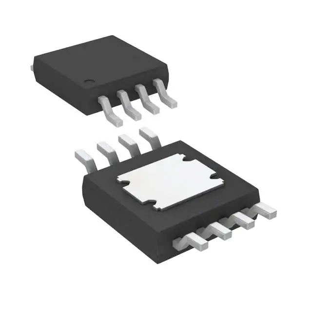
Ultrasmall package: 8-Lead MINI_SO_EP
APPLICATIONS
HMC220B
LO 1
8
RF
2
7
GND
GND 3
6
GND
NIC 4
5
IF
GND
NIC = NOT INTERNALLY CONNECTED
Very small aperture terminals (VSAT) and mobile satellite
communication terminals
Microwave and military radio
Wireless backhaul equipment
Automotive, dedicated short range communications (DSRC)
and intelligent vehicle highway systems (IVHS)
Military radar, electronic warfare (EW), and electronic
counter measure (ECM) subsystems
15769-001
FEATURES
Figure 1.
GENERAL DESCRIPTION
The HMC220B is an ultraminiature, double-balanced mixer in
an 8-lead mini small outline package with exposed pad
(MINI_SO_EP). This fundamental, monolithic microwave
integrated circuit (MMIC) mixer is constructed of gallium
arsenide (GaAs) Schottky diodes and planar transformer baluns
on the chip.
Rev. C
The device can be used as an upconverter, downconverter,
biphase demodulator, or phase comparator from 5 GHz to
12 GHz. The HMC220B provides excellent local oscillator (LO)
to radio frequency (RF) and LO to intermediate frequency (IF)
isolation due to optimized balun structures and operates as low as
7 dBm. The RoHS compliant HMC220B eliminates the need for
wire bonding and is compatible with high volume surfacemount manufacturing techniques.
Document Feedback
Information furnished by Analog Devices is believed to be accurate and reliable. However, no
responsibility is assumed by Analog Devices for its use, nor for any infringements of patents or other
rights of third parties that may result from its use. Specifications subject to change without notice. No
license is granted by implication or otherwise under any patent or patent rights of Analog Devices.
Trademarks and registered trademarks are the property of their respective owners.
One Technology Way, P.O. Box 9106, Norwood, MA 02062-9106, U.S.A.
Tel: 781.329.4700 ©2017–2019 Analog Devices, Inc. All rights reserved.
Technical Support
www.analog.com
�HMC220B
Data Sheet
TABLE OF CONTENTS
Features .............................................................................................. 1
Downconverter Performance ......................................................6
Applications ....................................................................................... 1
Upconverter Performance ......................................................... 10
Functional Block Diagram .............................................................. 1
Isolation and Return Loss ......................................................... 11
General Description ......................................................................... 1
IF Bandwidth .............................................................................. 13
Revision History ............................................................................... 2
Spurious Performance ............................................................... 15
Specifications..................................................................................... 3
Theory of Operation ...................................................................... 16
Absolute Maximum Ratings............................................................ 4
Applications Information .............................................................. 17
Thermal Resistance ...................................................................... 4
Evaluation PCB Information .................................................... 17
ESD Caution .................................................................................. 4
Typical Applications Circuit ..................................................... 17
Pin Configuration and Function Descriptions ............................. 5
Outline Dimensions ....................................................................... 18
Interface Schematics..................................................................... 5
Ordering Guide .......................................................................... 18
Typical Performance Characteristics ............................................. 6
REVISION HISTORY
10/2019—Rev. B to Rev. C
Changes to Table 1 ............................................................................ 3
Change to Table 2 and Table 3 ........................................................ 4
Updated Outline Dimensions ....................................................... 18
Changes to Ordering Guide .......................................................... 18
10/2017—Rev. 0 to Rev. A
Changes to LO to RF Parameter, Table 1........................................3
Changes to Figure 35 and Figure 38............................................. 11
Changes to Ordering Guide .......................................................... 18
7/2017—Revision 0: Initial Version
8/2018—Rev. A to Rev. B
Changes to Continuous Power Dissipation, PDISS Parameter
and Maximum Junction Temperature Parameter, Table 2 and
Table 3 ................................................................................................. 4
Rev. C | Page 2 of 18
�Data Sheet
HMC220B
SPECIFICATIONS
TA = 25°C, IF = 100 MHz, LO drive level = 10 dBm. All measurements performed as a downconverter with the lower sideband selected,
unless otherwise noted.
Table 1.
Parameter
FREQUENCY RANGE
Radio Frequency
Local Oscillator
Intermediate Frequency
LO DRIVE LEVEL
PERFORMANCE AT LO DRIVE = 10 dBm
Conversion Loss
Single Sideband (SSB) Noise Figure
Input Third-Order Intercept
Input Second-Order Intercept
Input 1 dB Compression Point
PERFORMANCE AT LO DRIVE = 13 dBm
Conversion Loss
SSB Noise Figure
Input Third-Order Intercept
Input Second-Order Intercept
Input 1 dB Compression Point
ISOLATION
RF to IF
LO to RF
LO to IF
Symbol
Min
RF
LO
IF
5
5
DC
7
NF
IIP3
IIP2
IP1dB
NF
IIP3
IIP2
IP1dB
Max
Unit
12
12
4
GHz
GHz
GHz
dBm
12
12
9.5
9.5
17
50
9.5
dB
dB
dBm
dBm
dBm
13
12
9
9
18.5
60
11
dB
dB
dBm
dBm
dBm
31
23
Rev. C | Page 3 of 18
Typ
10
20
40
38
dB
dB
dB
�HMC220B
Data Sheet
ABSOLUTE MAXIMUM RATINGS
THERMAL RESISTANCE
Table 2.
Parameter
RF Input Power
LO Input Power
IF Input Power
IF Source and Sink Current
Continuous Power Dissipation, PDISS
(TA = 85°C, Derate 5.5 mW/°C Above 85°C)
Junction Temperature
Peak Reflow Temperature (Moisture
Sensitivity Level (MSL1))1
Operating Temperature Range
Storage Temperature Range
Electrostatic Discharge (ESD) Sensitivity
Human Body Model (HBM)
Field Induced Charged Device Model (FICDM)
1
Rating
25 dBm
25 dBm
25 dBm
3 mA
495 mW
Thermal performance is directly linked to printed circuit board
(PCB) design and operating environment. Careful attention to
PCB thermal design is required.
175°C
260°C
1
Table 3. Thermal Resistance
Package Type
RH-8-11
θJA
104.7
θJC
180
Unit
°C/W
Thermal impedance simulated values are based on JEDEC 2S2P test board
with 3 mm × 3 mm thermal vias. See JEDEC JESD51-12 for additional information.
−40°C to +85°C
−65°C to +125°C
ESD CAUTION
2000 V (Class 2)
750 V (Class C4)
See the Ordering Guide section.
Stresses at or above those listed under Absolute Maximum
Ratings may cause permanent damage to the product. This is a
stress rating only; functional operation of the product at these
or any other conditions above those indicated in the
operational section of this specification is not implied.
Operation beyond the maximum operating conditions for
extended periods may affect product reliability.
Rev. C | Page 4 of 18
�Data Sheet
HMC220B
PIN CONFIGURATION AND FUNCTION DESCRIPTIONS
HMC220B
TOP VIEW
(Not to Scale)
LO 1
8
RF
GND 2
7
GND
GND 3
6
GND
NIC 4
5
IF
15769-002
NOTES
1. NIC = NOT INTERNALLY CONNECTED. THIS PIN CAN
BE LEFT FLOATING OR IT CAN BE SOLDERED DOWN
TO RF/DC GND. THE NIC PIN DOES NOT AFFECT THE
PERFORMANCE OF THE HMC220B.
2. EXPOSED PAD. CONNECT THE EXPOSED PAD TO A
LOW IMPEDANCE THERMAL AND ELECTRICAL
GROUND PLANE.
Figure 2. Pin Configuration
Table 4. Pin Function Descriptions
Pin No.
1
2, 3, 6, 7
4
Mnemonic
LO
GND
NIC
5
IF
8
RF
EPAD
Description
Local Oscillator. This pin is ac-coupled and matched to 50 Ω. See Figure 4 for the LO interface schematic.
Ground. Connect the package bottom to RF/dc ground. See Figure 3 for the GND interface schematic.
Not Internally Connected. This pin can be left floating or it can be soldered down to RF/dc GND. The NIC pin does
not affect the performance of the HMC220B.
Intermediate Frequency. This pin is dc-coupled. For applications not requiring operations to dc, dc block this
port externally using a series capacitor whose value is chosen to pass the necessary IF frequency range. For
operation to dc, this pin must not source or sink 3 mA of current, or the device is nonfunctioning and possible
device failure may result. See Figure 5 for the IF interface schematic.
Radio Frequency. This pin is ac-coupled internally and match to 50 Ω. See Figure 6 for the RF interface schematic.
Exposed Pad. Connect the exposed pad to a low impedance thermal and electrical ground plane.
INTERFACE SCHEMATICS
IF
15769-005
15769-003
Figure 3. GND Interface Schematic
15769-004
LO
Figure 5. IF Interface Schematic
RF
15769-006
GND
Figure 6. RF Interface Schematic
Figure 4. LO Interface Schematic
Rev. C | Page 5 of 18
�HMC220B
Data Sheet
TYPICAL PERFORMANCE CHARACTERISTICS
DOWNCONVERTER PERFORMANCE
Downconverter Performance at IF = 100 MHz, Lower Sideband
Data taken at LO = 10 dBm, TA = 25°C, unless otherwise noted.
0
0
+85°C
+25°C
–40°C
15dBm
13dBm
10dBm
9dBm
7dBm
–2
CONVERSION GAIN (dB)
CONVERSION GAIN (dB)
–4
–5
–10
–15
–6
–8
–10
–12
–14
–16
5
6
7
8
9
10
11
12
13
RF FREQUENCY (GHz)
–20
15769-007
5
10
11
12
13
9dBm
10dBm
13dBm
25
25
INPUT IP3 (dBm)
20
15
20
15
6
7
8
9
10
11
12
13
RF FREQUENCY (GHz)
10
15769-008
5
5
6
7
8
9
10
11
12
13
RF FREQUENCY (GHz)
Figure 8. Input IP3 vs. RF Frequency at Various Temperatures
15769-011
INPUT IP3 (dBm)
9
30
+85°C
+25°C
–40°C
Figure 11. Input IP3 vs. RF Frequency at Various LO Powers
100
100
+85°C
+25°C
–40°C
90
9dBm
10dBm
13dBm
90
80
INPUT IP2 (dBm)
80
70
60
50
70
60
50
40
40
30
30
5
6
7
8
9
10
11
12
13
RF FREQUENCY (GHz)
20
15769-009
INPUT IP2 (dBm)
8
Figure 10. Conversion Gain vs. RF Frequency at Various LO Powers
30
20
7
RF FREQUENCY (GHz)
Figure 7. Conversion Gain vs. RF Frequency at Various Temperature
10
6
5
6
7
8
9
10
11
12
RF FREQUENCY (GHz)
Figure 9. Input IP2 vs. RF Frequency at Various Temperatures
Figure 12. Input IP2 vs. RF Frequency at Various LO Powers
Rev. C | Page 6 of 18
13
15769-012
–20
15769-010
–18
�Data Sheet
HMC220B
20
20
10dBm
13dBm
+85°C
+25°C
–40°C
15
P1dB (dBm)
10
5
5
5
6
7
8
9
10
11
12
13
RF FREQUENCY (GHz)
0
15769-013
0
7dBm
10dBm
13dBm
25
20
15
10
5
6
7
8
9
10
11
12
13
RF FREQUENCY (GHz)
15769-014
NOISE FIGURE (dB)
30
5
6
7
8
9
10
11
12
13
Figure 15. Input P1dB vs. RF Frequency at Various LO Powers
40
35
5
RF FREQUENCY (GHz)
Figure 13. Input P1dB vs. RF Frequency at Various Temperatures
0
10
Figure 14. Noise Figure vs. RF Frequency at Various LO Powers
Rev. C | Page 7 of 18
15769-015
P1dB (dBm)
15
�HMC220B
Data Sheet
Downconverter Performance at IF = 1000 MHz, Lower Sideband
Data taken at LO = 10 dBm, TA = 25°C, unless otherwise noted.
0
0
+85°C
+25°C
–40°C
–5
CONVERSION GAIN (dB)
–10
–15
–20
–10
–15
–20
5
6
7
8
9
10
11
12
13
RF FREQUENCY (GHz)
–30
15769-016
9
10
11
12
13
7dBm
9dBm
10dBm
13dBm
15dBm
25
20
INPUT IP3 (dBm)
INPUT IP3 (dBm)
8
30
+85°C
+25°C
–40°C
25
15
10
20
15
10
5
5
6
7
8
9
10
11
12
13
0
15769-017
5
RF FREQUENCY (GHz)
5
6
7
8
9
10
11
12
13
RF FREQUENCY (GHz)
Figure 17. Input IP3 vs. RF Frequency at Various Temperatures
Figure 20. Input IP3 vs. RF Frequency at Various LO Powers
100
100
+85°C
+25°C
–40°C
90
80
70
70
INPUT IP2 (dBm)
80
60
50
40
60
50
40
30
30
20
20
10
10
5
6
7dBm
9dBm
10dBm
13dBm
90
7
8
9
10
11
12
13
RF FREQUENCY (GHz)
0
15769-018
INPUT IP2 (dBm)
7
Figure 19. Conversion Gain vs. RF Frequency at Various LO Powers
30
0
6
RF FREQUENCY (GHz)
Figure 16. Conversion Gain vs. RF Frequency at Various Temperatures
0
5
15769-020
–30
15769-019
–25
–25
5
6
7
8
9
10
11
12
RF FREQUENCY (GHz)
Figure 18. Input IP2 vs. RF Frequency at Various Temperatures
Figure 21. Input IP2 vs. RF Frequency at Various LO Powers
Rev. C | Page 8 of 18
13
15769-021
CONVERSION GAIN (dB)
–5
7dBm
9dBm
10dBm
13dBm
15dBm
�Data Sheet
HMC220B
Downconverter Performance at IF = 3000 MHz, Lower Sideband
Data taken at LO = 10 dBm, TA = 25°C, unless otherwise noted.
0
0
+85°C
+25°C
–40°C
–5
CONVERSION GAIN (dB)
–10
–15
–20
–10
–15
–20
–25
6
7
8
9
10
11
12
RF FREQUENCY (GHz)
–30
+85°C
+25°C
–40°C
9
10
12
11
9dBm
10dBm
13dBm
25
20
INPUT IP3 (dBm)
15
10
20
15
10
5
5
6
7
8
9
10
11
12
RF FREQUENCY (GHz)
0
15769-023
5
5
6
7
8
9
10
11
12
RF FREQUENCY (GHz)
Figure 23. Input IP3 vs. RF Frequency at Various Temperatures
15769-026
INPUT IP3 (dBm)
8
30
25
Figure 26. Input IP3 vs. RF Frequency at Various LO Powers
100
100
+85°C
+25°C
–40°C
90
80
9dBm
10dBm
13dBm
90
80
70
INPUT IP2 (dBm)
70
60
50
40
60
50
40
30
30
20
20
10
10
5
6
7
8
9
10
11
12
RF FREQUENCY (GHz)
0
15769-024
INPUT IP2 (dBm)
7
Figure 25. Conversion Gain vs. RF Frequency at Various LO Powers
30
0
6
RF FREQUENCY (GHz)
Figure 22. Conversion Gain vs. RF Frequency at Various Temperatures
0
5
15769-025
5
15769-022
–30
–25
5
6
7
8
9
10
11
12
RF FREQUENCY (GHz)
Figure 24. Input IP2 vs. RF Frequency at Various Temperatures
Figure 27. Input IP2 vs. RF Frequency at Various LO Powers
Rev. C | Page 9 of 18
15769-027
CONVERSION GAIN (dB)
–5
7dBm
9dBm
10dBm
13dBm
15dBm
�HMC220B
Data Sheet
UPCONVERTER PERFORMANCE
Upconverter Performance at IF = 100 MHz, Upper Sideband
Data taken at LO = 10 dBm, TA = 25°C, unless otherwise noted.
0
0
7dBm
9dBm
10dBm
11dBm
13dBm
–15
5
6
7
8
9
10
11
12
13
RF FREQUENCY (GHz)
–10
–15
–20
9
10
11
12
13
7dBm
9dBm
10dBm
11dBm
13dBm
25
20
INPUT IP3 (dBm)
15
10
20
15
10
6
7
8
9
10
11
12
13
RF FREQUENCY (GHz)
0
15769-029
5
5
6
7
8
9
10
11
12
13
RF FREQUENCY (GHz)
Figure 29. Input IP3 vs. RF Frequency at Various Temperatures
15769-032
5
5
Figure 32. Input IP3 vs. RF Frequency at Various LO Powers
80
80
+85°C
+25°C
–40°C
70
7dBm
9dBm
10dBm
11dBm
13dBm
70
60
INPUT IP2 (dBm)
60
50
40
30
50
40
30
20
20
10
10
6
7
8
9
10
11
12
13
RF FREQUENCY (GHz)
0
15769-030
5
5
6
7
8
9
10
11
12
RF FREQUENCY (GHz)
Figure 30. Input IP2 vs. RF Frequency at Various Temperatures
Figure 33. Input IP2 vs. RF Frequency at Various LO Powers
Rev. C | Page 10 of 18
13
15769-033
INPUT IP3 (dBm)
8
30
+85°C
+25°C
–40°C
25
INPUT IP2 (dBm)
7
Figure 31. Conversion Gain vs. RF Frequency at Various LO Powers
30
0
6
RF FREQUENCY (GHz)
Figure 28. Conversion Gain vs. RF Frequency at Various Temperatures
0
5
15769-031
–10
–20
–5
CONVERSION GAIN (dB)
–5
15769-028
CONVERSION GAIN (dB)
+85°C
+25°C
–40°C
�Data Sheet
HMC220B
ISOLATION AND RETURN LOSS
Data taken at IF = 100 MHz, LO = 10 dBm, TA = 25°C, unless otherwise noted.
70
70
+85°C
+25°C
–40°C
60
ISOLATION (dB)
50
30
40
30
20
20
10
10
5
6
7
8
9
10
11
12
13
LO FREQUENCY (GHz)
0
Figure 34. LO to IF Isolation vs. LO Frequency at Various Temperatures
9
10
11
12
13
50
40
40
ISOLATION (dB)
30
20
7dBm
9dBm
10dBm
13dBm
15dBm
30
20
6
7
8
9
10
11
12
13
LO FREQUENCY (GHz)
0
15769-035
5
Figure 35. LO to RF Isolation vs. LO Frequency at Various Temperatures
5
6
7
8
9
10
11
12
15769-038
10
13
LO FREQUENCY (GHz)
Figure 38. LO to RF Isolation vs. LO Frequency at Various LO Powers
30
30
+85°C
+25°C
–40°C
25
7dBm
9dBm
10dBm
13dBm
15dBm
25
ISOLATION (dB)
20
15
10
5
20
15
10
5
6
7
8
9
10
RF FREQUENCY (GHz)
11
12
13
0
15769-036
5
Figure 36. RF to IF Isolation vs. RF Frequency at Various Temperatures
5
6
7
8
9
10
11
12
13
RF FREQUENCY (GHz)
Figure 39. RF to IF Isolation vs. RF Frequency at Various LO Powers
Rev. C | Page 11 of 18
15769-039
ISOLATION (dB)
8
60
10
ISOLATION (dB)
7
Figure 37. LO to IF Isolation vs. LO Frequency at Various LO Powers
+85°C
+25°C
–40°C
50
0
6
LO FREQUENCY (GHz)
60
0
5
15769-037
40
15769-034
ISOLATION (dB)
50
0
+7dBm
+9dBm
+10dBm
+13dBm
+15dBm
60
�Data Sheet
0
0
–5
–5
IF RETURN LOSS (dB)
–10
–15
–20
–15
–20
3
4
5
6
7
8
9
10
11
12
13
LO FREQUENCY (GHz)
–25
15769-040
–25
0
–5
–10
–15
–25
5
6
7
8
9
10
11
RF FREQUENCY (GHz)
12
13
15769-041
–20
4
2
3
Figure 42. IF Return Loss vs. IF Frequency
0
3
1
IF FREQUENCY (GHz)
Figure 40. LO Return Loss vs. LO Frequency
RF RETURN LOSS (dB)
–10
Figure 41. RF Return Loss vs. RF Frequency
Rev. C | Page 12 of 18
4
15769-042
LO RETURN LOSS (dB)
HMC220B
�Data Sheet
HMC220B
IF BANDWIDTH
Downconverter Performance, Lower Sideband
Data taken at LO = 10 dBm, TA =25°C, unless otherwise noted.
0
7dBm
9dBm
10dBm
11dBm
13dBm
CONVERSION GAIN (dB)
–5
–10
–15
–20
0
0.5
1.0
1.5
2.0
2.5
3.0
3.5
IF FREQUENCY (GHz)
–15
0
0.5
1.0
1.5
2.0
2.5
3.0
3.5
Figure 45. Conversion Gain vs. IF Frequency at Various LO Drives
30
30
+85°C
+25°C
–40°C
25
7dBm
9dBm
10dBm
11dBm
13dBm
25
INPUT IP3 (dBm)
20
15
10
20
15
10
5
0
0.5
1.0
1.5
2.0
2.5
3.0
3.5
IF FREQUENCY (GHz)
0
0
0.5
1.0
1.5
2.0
2.5
3.0
IF FREQUENCY (GHz)
Figure 44. Input IP3 vs. IF Frequency at Various Temperatures
Figure 46. Input IP3 vs. IF Frequency at Various LO Drives
Rev. C | Page 13 of 18
3.5
15769-046
5
15769-044
INPUT IP3 (dBm)
–10
IF FREQUENCY (GHz)
Figure 43. Conversion Gain vs. IF Frequency at Various Temperatures
0
–5
–20
15769-043
CONVERSION GAIN (dB)
+85°C
+25°C
–40°C
15769-045
0
�HMC220B
Data Sheet
Downconverter Performance, Upper Sideband
Data taken at LO = 10 dBm, TA = 25°C, unless otherwise noted.
0
7dBm
9dBm
10dBm
11dBm
13dBm
CONVERSION GAIN (dB)
–5
–10
–15
0
1
2
3
4
5
6
IF FREQUENCY (GHz)
0
1
2
3
4
5
6
IF FREQUENCY (GHz)
Figure 49. Conversion Gain vs. IF Frequency at Various LO Drives
30
30
+85°C
+25°C
–40°C
25
25
INPUT IP3 (dBm)
20
15
10
20
15
10
7dBm
9dBm
10dBm
11dBm
13dBm
5
5
0
1
2
3
4
5
6
IF FREQUENCY (GHz)
15769-048
INPUT IP3 (dBm)
–15
–20
Figure 47. Conversion Gain vs. IF Frequency at Various Temperatures
0
–10
Figure 48. Input IP3 vs. IF Frequency at Various Temperatures
0
0
1
2
3
4
5
IF FREQUENCY (GHz)
Figure 50. Input IP3 vs. IF Frequency at Various LO Drives
Rev. C | Page 14 of 18
6
15769-050
–20
–5
15769-047
CONVERSION GAIN (dB)
+85°C
+25°C
–40°C
15769-049
0
�Data Sheet
HMC220B
SPURIOUS PERFORMANCE
Mixer spurious products are measured in decibels relative to
carrier from the IF output power level, unless otherwise noted.
RF = 12000 MHz, LO = 12100 MHz, LO power = +10 dBm, RF
power = −10 dBm.
Spur values are (M × RF) − (N × LO).
Harmonics of LO
LO Power = 10 dBm. Values are in decibels relative to carrier
(dBc) below the input LO level measured at the RF port.
0
1
2
3
4
5
M × RF
NLO Spur at RF
Port(dBc)
LO Frequency
(GHz)
6
7
9
10
12
13
1
1
42
36
39
43
36
33
2
42
47
44
55
65
57
3
57
52
72
52
72
60
4
91
51
71
76
84
N/A1
1
M × RF
1
0
1
2
3
4
5
N × LO
3
31
29
62
50
89
87
4
52
40
64
52
88
79
5
56
43
71
65
84
78
RF = 8500 MHz, LO = 8600 MHz, LO power = +10 dBm, RF
power = −10 dBm.
M × RF
1
M × RF
1
0
1
2
3
4
5
1
2
0
49
82
87
85
2
28
23
57
75
88
86
N × LO
3
29
46
46
69
89
88
4
54
68
83
68
96
95
4
56
62
86
77
94
87
5
0
61
75
86
89
95
5
46
50
82
85
86
95
0
N/A1
−6
+41
+40
+46
+67
0
1
2
3
4
5
1
−3
0
+35
+27
+53
+63
2
+18
+6
+31
+5
+31
+39
N × LO
3
+31
+5
+31
+6
+18
+18
4
+53
+27
+35
0
−3
−3
5
+46
+40
+41
−6
0
−6
N/A means not applicable.
RF = 8500 MHz, LO = 9500 MHz, LO power = +10 dBm, RF
power = −10 dBm.
N/A means not applicable.
0
N/A1
12
80
88
82
80
N × LO
3
39
59
80
61
89
85
RF = 5000 MHz, LO = 6000 MHz, LO power = +10 dBm, RF
power = −10 dBm.
RF = 5000 MHz, LO = 5100 MHz, LO power = +10 dBm, RF
power = −10 dBm.
2
25
12
60
49
88
85
2
35
26
69
77
87
75
M × N Spurious Outputs, IF = 1000 MHz
M × N Spurious Outputs, IF = 100 MHz
1
7
0
63
60
85
84
1
20
0
63
84
76
63
N/A means not applicable.
N/A means not applicable.
0
N/A1
5
57
77
83
82
0
N/A1
9
85
75
62
0
M × RF
1
0
N/A1
+11
+88
+87
+84
+81
0
1
2
3
4
5
1
−3
0
+58
+82
+84
+87
2
+24
+21
+60
+84
+90
+87
N × LO
3
+28
+40
+47
+71
+94
+89
4
+48
+62
+64
+72
+95
+87
5
+49
+52
+77
+80
+95
+95
N/A means not applicable.
RF = 12000 MHz, LO = 13000 MHz, LO power = +10 dBm, RF
power = −10 dBm.
N/A means not applicable.
M × RF
1
0
1
2
3
4
5
0
N/A1
10
84
75
64
0
N/A means not applicable.
Rev. C | Page 15 of 18
1
14
0
64
84
71
67
2
42
28
83
84
82
73
N × LO
3
29
63
61
75
85
85
4
55
55
81
73
93
87
5
0
60
77
80
87
88
�HMC220B
Data Sheet
THEORY OF OPERATION
The HMC220B is a general-purpose, double balanced mixer in an
8-lead MINI_SO_EP, RoHS compliant package that can be used as
an upconverter or a downconverter from 5 GHz to 12 GHz.
When used as a downconverter, the HMC220B downconverts
RF between 5 GHz to 12 GHz to IF between dc and 4 GHz.
When used as an upconverter, the mixer upconverts IF between
dc and 4 GHz to RF between 5 GHz and 12 GHz.
The mixer provides excellent LO to RF and LO to IF isolation
due to optimized balun structures. The HMC220B requires no
external components or matching circuitry. The RoHS
compliant HMC220B eliminates the need for wire bonding and
is compatible with high volume, surface-mount manufacturing
techniques.
Rev. C | Page 16 of 18
�Data Sheet
HMC220B
APPLICATIONS INFORMATION
TYPICAL APPLICATIONS CIRCUIT
HMC220B
The PCB used in this application must use RF circuit design
techniques. Signal lines must have 50 Ω impedance, and the
package ground lead and exposed pad must be connected
directly to the ground planes. The evaluation PCB shown in
Figure 52 is available from Analog Devices, Inc., upon request.
LO
1
RF
8
2
7
3
6
4
5
IF
15769-051
EVALUATION PCB INFORMATION
15769-052
Figure 51. Typical Applications Circuit
Figure 52. EV1HMC220BMS8G Evaluation PCB
Table 5. EV1HMC220BMS8G PCB Components
Item
1
2
3
Description
PCB, EV1HMC220BMS8G
2.92 mm Subminiature Version A (SMA) connector
SMA connector, end launch
4
Device under test (DUT)
Reference
Designator
J1, J2
J3
Quantity
1
2
1
U1
1
Rev. C | Page 17 of 18
Manufacturer
Analog Devices
SRI Connector Gage
Cinch Connectivity
Solutions Johnson
Analog Devices
Part Number
101828-8
21-146-1000-01
142-0701-851
HMC220BMS8GE
�HMC220B
Data Sheet
OUTLINE DIMENSIONS
3.10
3.00
2.90
8
0.65
BSC
0.94
0.86
0.78
PKG-003371
0.13
MAX
COPLANARITY
0.10
5
1
5.05
4.90
4.75
1.83
1.73
1.63
EXPOSED
PAD
4
TOP VIEW
FOR PROPER CONNECTION OF
THE EXPOSED PAD, REFER TO
THE PIN CONFIGURATION AND
FUNCTION DESCRIPTIONS
SECTION OF THIS DATA SHEET.
BOTTOM VIEW
1.95 BSC
1.10
MAX
SIDE VIEW
0.25 GAGE
PLANE
6°
0°
0.40
0.33
0.25
END VIEW
0.70
0.55
0.40
0.23
0.08
0.95
REF
COMPLIANT TO JEDEC STANDARDS MO-187-AA-T
08-02-2019-B
3.10
3.00
2.90
2.26
2.16
2.06
Figure 53. 8-Lead Mini Small Outline Package with Exposed Pad [MINI_SO_EP]
(RH-8-1)
Dimensions shown in millimeters
ORDERING GUIDE
Model1
HMC220BMS8GE
HMC220BMS8GETR
EV1HMC220BMS8G
1
2
Temperature
Range
−40°C to +85°C
−40°C to +85°C
MSL
Rating2
MSL1
MSL1
Package Description
8-Lead Mini Small Outline Package with Exposed Pad [MINI_SO_EP]
8-Lead Mini Small Outline Package with Exposed Pad [MINI_SO_EP]
Evaluation PCB Assembly
The HMC220BMS8GE and HMC220BMS8GETR are RoHS Compliant Parts.
See the Absolute Maximum Ratings section.
©2017–2019 Analog Devices, Inc. All rights reserved. Trademarks and
registered trademarks are the property of their respective owners.
D15769-0-10/19(C)
Rev. C | Page 18 of 18
Package
Option
RH-8-1
RH-8-1
�