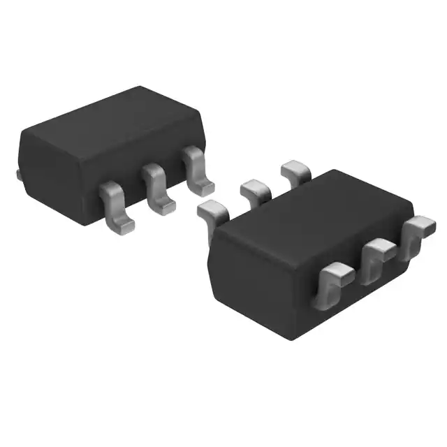
HMC291SE
v05.1216
ATTENUATORS - ANALOG - SMT
4 dB LSB SILICON 2-BIT POSITIVE CONTROL
DIGITAL ATTENUATOR, 0.7 - 4.0 GHz
Typical Applications
Features
The HMC291SE is ideal for:
RoHS Compliant Product
• Cellular
4 dB LSB Steps to 12 dB
• PCS, ISM, MMDS
Single Positive Control Per Bit, 0/+3V or +5V
• WLL Handset & Base Station
Typical Step Error : ±0.3 dB
Miniature SOT 26 Package: 9 mm2
Functional Diagram
General Description
The HMC291SE is a general purpose broadband
2-bit positive control silicon IC digital attenuator in
6 lead SOT26 surface mount plastic package. The
insertion loss is typically in between 0.4 dB - 1 dB
through operating frequency range. The attenuator
bit values are 4 (LSB) and 8 dB for a total attenuation
of 12 dB. State error is excellent at ± 0.4 dB typical
with an IIP3 of up to 57 dBm. Two bit control voltage
inputs, toggled between 0V and +3V or +5V, are used
to select each attenuation state at less than 25 µA
each. A single VDD supply voltage of +3V to +5V
applied through an external 4.7K Ohm resistor is
required.
Electrical Specifications,
TA = +25°C, VDD = +3V to +5V & VCTL = 0/VDD (Unless Otherwise Stated)
Parameter
Frequency
Min.
Typical
Max.
Units
0.65
0.65
0.7
1.32
dB
dB
dB
dB
Insertion Loss
0.7 - 1.4 GHz
1.4 - 2.3 GHz
2.3 - 2.7 GHz
2.7 - 4.0 GHz
0.5
0.5
0.6
0.8
Attenuation Range
0.7 - 4.0 GHz
12
dB
Return Loss
(RF1 & RF2, All Atten. States)
0.7 - 1.4 GHz
1.4 - 4.0 GHz
25
27
dB
dB
0.7 - 1.4 GHz
1.4 - 2.3 GHz
2.3 - 2.7 GHz
2.7 - 4.0 GHz
± (0.1 + 4% of Atten. Setting Max)
± (0.2 + 2% of Atten. Setting Max)
± (0.4 + 3% of Atten. Setting Max)
± (0.4 + 4% of Atten. Setting Max)
dB
dB
dB
dB
[1]
0.7 - 4.0 GHz
28
27
dBm
dBm
5V
3V
0.7 - 4.0 GHz
20
17
State Error
All Attenuation States
All Attenuation States
All Attenuation States
All Attenuation States
Input Power for 0.1 dB Compression (Input P0.1dB)
Input Third Order Intercept Point (IIP3)
(Two-tone Input Power = 15 dBm Each Tone)
Switching Characteristics
tRISE, tFALL (10/90% RF)
tON, tOFF (50% CTL to 10/90% RF)
5V
3V
52
52
57
54
59
56
dBm
dBm
0.7 - 4.0 GHz
250
300
ns
ns
[1] Compression point is above maximum input power
1
Information furnished by Analog Devices is believed to be accurate and reliable. However, no
responsibility is assumed by Analog Devices for its use, nor for any infringements of patents or other
rights of third parties that may result from its use. Specifications subject to change without notice. No
license is granted by implication or otherwise under any patent or patent rights of Analog Devices.
Trademarks and registered trademarks are the property of their respective owners.
For price, delivery, and to place orders: Analog Devices, Inc.,
One Technology Way, P.O. Box 9106, Norwood, MA 02062-9106
Phone: 781-329-4700 • Order online at www.analog.com
Application Support: Phone: 1-800-ANALOG-D
�HMC291SE
v05.1216
4 dB LSB SILICON 2-BIT POSITIVE CONTROL
DIGITAL ATTENUATOR, 0.7 - 4.0 GHz
Insertion Loss
Return Loss RF1, RF2
RETURN LOSS (dB)
INSERTION LOSS (dB)
-15
-0.5
-1
-20
-25
-30
-35
-40
-45
-1.5
0.5
0.5
1
1.5
2
2.5
3
3.5
1
1.5
4
2
2.5
3
3.5
4
FREQUENCY (GHz)
FREQUENCY (GHz)
+25C
+85C
RF1 - IL
RF1 - 4 dB
RF1 - 8 dB
-40C
0.6
-2
0.4
0.2
-4
-6
-8
-10
0
-0.2
-0.4
-0.6
-12
-0.8
-14
-1
0.5
1
1.5
2
2.5
3
3.5
4
0.5
1
1.5
FREQUENCY (GHz)
4 dB
2
2.5
3
3.5
4
FREQUENCY (GHz)
8 dB
12 dB
4 dB
Step Error vs. Frequency
8 dB
12 dB
Relative Phase vs. Frequency
0.6
60
0.4
50
0.2
40
RELATIVE PHASE (deg.)
STEP ERROR (dB)
RF2 - 8 dB
RF2 - 12 dB
State Error vs. Attenuation State
0
STATE ERROR (dB)
NORMALIZED ATTENUATION (dB)
Normalized Attenuation vs. Attenuation State
RF1 - 12 dB
RF2 - IL
RF2 - 4 dB
ATTENUATORS - ANALOG - SMT
-10
0
0
-0.2
-0.4
30
20
10
-0.6
0
-0.8
-10
-1
-20
0.5
1
1.5
2
2.5
3
3.5
4
0.5
1
1.5
4 dB
8 dB
2
2.5
3
3.5
4
FREQUENCY (GHz)
FREQUENCY (GHz)
12 dB
4 dB
8 dB
12 dB
For price, delivery, and to place orders: Analog Devices, Inc., One Technology Way, P.O. Box 9106, Norwood, MA 02062-9106
Phone: 781-329-4700 • Order online at www.analog.com
Application Support: Phone: 1-800-ANALOG-D
2
�HMC291SE
v05.1216
4 dB LSB SILICON 2-BIT POSITIVE CONTROL
DIGITAL ATTENUATOR, 0.7 - 4.0 GHz
30
30
29
29
28
28
INPUT COMPRESSION (dBm)
INPUT COMPRESSION (dBm)
Input P0.1dB vs. Frequency at 5V over
Temperature[1]
27
26
25
24
23
22
21
27
26
25
24
23
22
21
20
20
0.7
1
1.3
1.6
1.9
2.2
2.5
2.8
3.1
3.4
3.7
4
0.7
1
1.3
1.6
FREQUENCY (GHz)
+25C
1.9
2.2
2.5
2.8
3.1
3.4
3.7
+85C
-40C
+25C
+85C
-40C
IIP3 vs. Frequency at 5V over
Temperature
65
64
64
63
63
62
62
61
61
60
60
IIP3 (dBm)
65
59
58
57
56
59
58
57
56
55
55
54
54
53
53
52
52
51
51
50
50
0.7
1
1.3
1.6
1.9
2.2
2.5
2.8
3.1
3.4
3.7
4
0.7
1
1.3
FREQUENCY (GHz)
+25C
+85C
1.6
1.9
2.2
2.5
2.8
3.1
3.4
3.7
FREQUENCY (GHz)
-40C
+25C
+85C
-40C
[1] Input P0.1dB is limited by maximum test power of 28 dBm.
3
4
FREQUENCY (GHz)
IIP3 vs. Frequency at 3V over
Temperature
IIP3 (dBm)
ATTENUATORS - ANALOG - SMT
Input P0.1dB vs. Frequency at 3V over
Temperature
For price, delivery, and to place orders: Analog Devices, Inc., One Technology Way, P.O. Box 9106, Norwood, MA 02062-9106
Phone: 781-329-4700 • Order online at www.analog.com
Application Support: Phone: 1-800-ANALOG-D
4
�HMC291SE
v05.1216
4 dB LSB SILICON 2-BIT POSITIVE CONTROL
DIGITAL ATTENUATOR, 0.7 - 4.0 GHz
ATTENUATORS - ANALOG - SMT
Application Circuit
DC blocking capacitors C1 and C2 are required on RF1
and RF2. Choose C1 = C2 = 100 ~ 300 pF to allow
lowest frequency of operation to pass with minimal loss.
R1 = 4.7K Ohm is required to supply voltage to the circuit
through either PIN 3 or PIN 1.
Evaluation Circuit Board
List of Materials for Evaluation PCB EV1HMC291SE [1]
Item
Description
J1 - J2
PCB Mount SMA Connector
J5 - J8
DC Pin
R1
4.7 kOhm Resistor, 0402 Pkg.
C1, C2
0402 Pkg. Capacitor, Select for Lowest
Frequency of Operation
C3
1 nF capacitor, 0402 Pkg.
U1
HMC291SE Digital Attenuator
PCB [2]
103370 Evaluation PCB 1.5” x 1.5”
[1] Reference this number when ordering complete evaluation PCB
The circuit board used in the application should use
RF circuit design techniques. Signal lines should
have 50 Ohm impedance while the package ground
leads should be connected directly to the ground
plane similar to that shown. A sufficient number
of via holes should be used to connect the top and
bottom ground planes. The evaluation circuit board
as shown is available from Analog Devices upon
request.
[2] Circuit Board Material: Rogers 4350
For price, delivery, and to place orders: Analog Devices, Inc., One Technology Way, P.O. Box 9106, Norwood, MA 02062-9106
Phone: 781-329-4700 • Order online at www.analog.com
Application Support: Phone: 1-800-ANALOG-D
4
�HMC291SE
v05.1216
4 dB LSB SILICON 2-BIT POSITIVE CONTROL
DIGITAL ATTENUATOR, 0.7 - 4.0 GHz
ATTENUATORS - ANALOG - SMT
Truth Table
Control & Bias Voltages
Control Voltage Input (VCTL)
V1
8 dB
V2
4 dB
Attenuation
Setting
RF1 - RF2
High
High
Reference I.L.
High
Low
4 dB
Low
High
8 dB
Low
12 dB
Max. Atten.
Low
State
Bias Condition
Low
0 to +0.2V at 500 µA Max.
High
VDD ± 0.2V at 550 µA Max.
Note: VDD = +3V to 5V with ± 0.2V tolerance
Absolute Maximum Ratings
Any combination of the above states will provide an attenuation
approximately equal to the sum of the bits selected.
ELECTROSTATIC SENSITIVE DEVICE
OBSERVE HANDLING PRECAUTIONS
Control Voltage (V1, V2)
VDD + 0.5 VDC
RF Input Power
+28 dBm
Bias Voltage (VDD)
+8.0 Vdc
Storage Temperature
-65°C to +150°C
Operating Temperature
-40°C to +85°C
ESD Sensitivity (HBM)
Class 1C
ESD Sensitivity (FICDM)
Class IV
Outline Drawing
NOTES:
1. PACKAGE BODY MATERIAL: LOW STRESS INJECTION MOLDED PLASTIC SILICA AND
SILICON IMPREGNATED.
2. LEAD MATERIAL: COPPER ALLOY.
3. LEAD PLATING: 100% MATTE TIN.
4. DIMENSIONS ARE IN INCHES [MILLIMETERS].
5. CHARACTERS TO BE HELVETICA MEDIUM, .030 HIGH, LASER OR WHITE INK,
LOCATED
APPROXIMATELY AS SHOWN.
6. DIMENSION DOES NOT INCLUDE MOLDFLASH OF 0.15mm PER SIDE.
7. DIMENSION DOES NOT INCLUDE MOLDFLASH OF 0.25mm PER SIDE.
8. ALL GROUND LEADS MUST BE SOLDERED TO PCB RF GROUND.
Package Information
Part Number
Package Body Material
Lead Finish
HMC291SE
RoHS-compliant Low Stress Injection Molded Plastic
100% matte Sn
MSL Rating
MSL1
[2]
Package Marking
[1]
291S
XXXX
[1] XXXX 4 digit lot number is on the bottom of package
[2] Max peak reflow temperature of 260°C
5
For price, delivery, and to place orders: Analog Devices, Inc., One Technology Way, P.O. Box 9106, Norwood, MA 02062-9106
Phone: 781-329-4700 • Order online at www.analog.com
Application Support: Phone: 1-800-ANALOG-D
�