HMC331
v04.1007
Features
The HMC331 is suitable for:
Conversion Loss: 14 dB
• Wireless Local Loop
Fo, 3Fo, 4Fo Isolation: 50 dB
• LMDS, VSAT, and Point-to-Point Radios
Passive: No Bias Required
• Test Equipment
Die Size: 0.85 x 0.55 x 0.1 mm
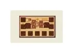
Functional Diagram
General Description
TE
Typical Applications
B
SO
LE
The HMC331 is a passive miniature frequency
doubler MMIC. Suppression of undesired fundamental
and higher order harmonics is 50 dB typical with
respect to input signal level. The doubler utilizes the
same GaAs Schottky diode/balun technology found
in Hittite MMIC mixers. It features small size, requires
no DC bias, and adds no measurable additive phase
noise onto the multiplied signal.
Electrical Specifi cations, TA = +25° C, As a Function of Drive Level
O
FREQUENCY MULTIPLIERS - PASSIVE - CHIP
2
Parameter
Input = +11 dBm
Min.
Typ.
Input = +13 dBm
Max.
Min.
Typ.
Input = +15 dBm
Max.
Min.
Typ.
Frequency Range, Input
13 - 18
12 - 18
12 - 18
Frequency Range, Output
26 - 36
24 - 36
24 - 36
Conversion Loss
2 - 22
GaAs MMIC PASSIVE FREQUENCY
DOUBLER, 12 - 18 GHz INPUT
15
20
14
20
14
Max.
Units
GHz
GHz
19
dB
FO Isolation
(with respect to input level)
45
50
45
50
45
50
dB
3FO Isolation
(with respect to input level)
50
60
45
60
47
60
dB
4FO Isolation
(with respect to input level)
50
60
50
60
50
60
dB
For price,
delivery,
and to place
orders: Analog Devices, Inc.,
For price, delivery, and to place orders, please contact
Hittite
Microwave
Corporation:
One Technology Way, P.O. Box 9106, Norwood, MA 02062-9106
20 Alpha Road, Chelmsford, MA 01824 Phone: Phone:
978-250-3343
978-250-3373
781-329-4700Fax:
• Order
online at www.analog.com
Application Support: Phone: 1-800-ANALOG-D
Order On-line at www.hittite.com
Information furnished by Analog Devices is believed to be accurate and reliable. However, no
responsibility is assumed by Analog Devices for its use, nor for any infringements of patents or other
rights of third parties that may result from its use. Specifications subject to change without notice. No
license is granted by implication or otherwise under any patent or patent rights of Analog Devices.
Trademarks and registered trademarks are the property of their respective owners.
�HMC331
v04.1007
GaAs MMIC PASSIVE FREQUENCY
DOUBLER, 12 - 18 GHz INPUT
Conversion Loss
@ 25 C Vs. Drive Level
CONVERSION GAIN (dB)
+ 25 C
+ 85 C
-55 C
-5
-10
-5
+ 15 dBm
+ 13 dBm
+ 11 dBm
-10
-15
-20
TE
-15
-20
-25
-25
-30
12
13
14
15
16
17
18
12
Isolation @ +15 dBm Drive Level*
13
14
15
16
17
18
FREQUENCY (GHz)
LE
INPUT FREQUENCY (GHz)
Input Return Loss vs. Drive Level
0
0
Fo
3Fo
4Fo
-40
-60
-80
-100
10
-5
B
SO
-20
ISOLATION (dB)
2
0
15
20
25
30
35
40
45
50
RETURN LOSS (dB)
CONVERSION GAIN (dB)
0
-10
-15
+ 15 dBm
+ 13 dBm
+ 11 dBm
-20
-25
-30
12
13
14
15
16
17
18
FREQUENCY (GHz)
FREQUENCY (GHz)
*With respect to input level
Output Return Loss
For Three Input Frequencies
O
Absolute Maximum Ratings
RETURN LOSS (dB0
0
13 GHz In
15 GHz In
18 GHz In
-6
Input Drive
+27 dBm
Storage Temperature
-65 to +150 °C
Operating Temperature
-55 to +85 °C
FREQUENCY MULTIPLIERS - PASSIVE - CHIP
Conversion Loss vs.
Temperature @ +15 dBm Drive Level
-12
ELECTROSTATIC SENSITIVE DEVICE
OBSERVE HANDLING PRECAUTIONS
-18
-24
-30
22
24
26
28
30
32
34
36
OUTPUT FREQUENCY (GHz)
For price,
delivery,
and to place
orders: Analog Devices, Inc.,
For price, delivery, and to place orders, please contact
Hittite
Microwave
Corporation:
One Technology Way, P.O. Box 9106, Norwood, MA 02062-9106
20 Alpha Road, Chelmsford, MA 01824 Phone: Phone:
978-250-3343
978-250-3373
781-329-4700Fax:
• Order
online at www.analog.com
Application Support: Phone: 1-800-ANALOG-D
Order On-line at www.hittite.com
Information furnished by Analog Devices is believed to be accurate and reliable. However, no
responsibility is assumed by Analog Devices for its use, nor for any infringements of patents or other
rights of third parties that may result from its use. Specifications subject to change without notice. No
license is granted by implication or otherwise under any patent or patent rights of Analog Devices.
Trademarks and registered trademarks are the property of their respective owners.
2 - 23
�HMC331
v04.1007
GaAs MMIC PASSIVE FREQUENCY
DOUBLER, 12 - 18 GHz INPUT
Outline Drawing
2 - 24
TE
LE
Die Packaging Information [1]
Standard
Alternate
GP-5 (Gel Pack)
[2]
NOTES:
1. ALL DIMENSIONS ARE IN INCHES [MM]
2. DIE THICKNESS IS .004”
3. TYPICAL BOND IS .004” SQUARE
4. BACKSIDE METALLIZATION: GOLD
5. BOND PAD METALLIZATION: GOLD
6. BACKSIDE METAL IS GROUND.
7. CONNECTION NOT REQUIRED FOR
UNLABELED BOND PADS.
B
SO
[1] Refer to the “Packaging Information” section for die
packaging dimensions.
[2] For alternate packaging information contact Hittite
Microwave Corporation.
Pad Description
O
FREQUENCY MULTIPLIERS - PASSIVE - CHIP
2
Pad Number
Function
Description
1
RFIN
DC coupled and matched to 50 Ohm.
2
RFOUT
DC coupled and matched to 50 Ohm.
Die Bottom
GND
Die bottom must be connected to RF/DC ground.
Interface Schematic
For price,
delivery,
and to place
orders: Analog Devices, Inc.,
For price, delivery, and to place orders, please contact
Hittite
Microwave
Corporation:
One Technology Way, P.O. Box 9106, Norwood, MA 02062-9106
20 Alpha Road, Chelmsford, MA 01824 Phone: Phone:
978-250-3343
978-250-3373
781-329-4700Fax:
• Order
online at www.analog.com
Application Support: Phone: 1-800-ANALOG-D
Order On-line at www.hittite.com
Information furnished by Analog Devices is believed to be accurate and reliable. However, no
responsibility is assumed by Analog Devices for its use, nor for any infringements of patents or other
rights of third parties that may result from its use. Specifications subject to change without notice. No
license is granted by implication or otherwise under any patent or patent rights of Analog Devices.
Trademarks and registered trademarks are the property of their respective owners.
�HMC331
v04.1007
GaAs MMIC PASSIVE FREQUENCY
DOUBLER, 12 - 18 GHz INPUT
Mounting & Bonding Techniques for Millimeterwave GaAs MMICs
50 Ohm Microstrip transmission lines on 0.127mm (5 mil) thick alumina thin film
substrates are recommended for bringing RF to and from the chip (Figure 1). If
0.254mm (10 mil) thick alumina thin film substrates must be used, the die should be
raised 0.150mm (6 mils) so that the surface of the die is coplanar with the surface
of the substrate. One way to accomplish this is to attach the 0.102mm (4 mil) thick
die to a 0.150mm (6 mil) thick molybdenum heat spreader (moly-tab) which is then
attached to the ground plane (Figure 2).
0.102mm (0.004”) Thick GaAs MMIC
0.076mm
(0.003”)
TE
RF Ground Plane
Microstrip substrate should be brought as close to the die as possible in order to
minimize ribbon bond length. Typical die-to-substrate spacing is 0.076mm (3 mils).
Gold ribbon of 0.075mm ( 3 mil) width and minimal length