HMC346LC3B
v06.0514
ATTENUATORS - ANALOG - SMT
GaAs MMIC VOLTAGE-VARIABLE
ATTENUATOR, DC - 18 GHz
Typical Applications
Features
The HMC346LC3B is ideal for:
Wide Bandwidth: DC - 18 GHz
• Test Instrumentation
Low Phase Shift vs. Attenuation
• Fiber Optics & Broadband Telecom
30 dB Attenuation Range
• Microwave Radio & VSAT
Simplified Voltage Control
• Military Radios, Radar, & ECM
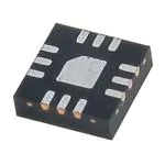
RoHS Compliant 3 x 3 mm SMT Package
Functional Diagram
General Description
The HMC346LC3B is an absorptive Voltage Variable
Attenuator (VVA) in a leadless “Pb free” RoHS
compliant SMT mount ceramic package operating from
DC - 18 GHz. It features an on-chip reference
attenuator for use with an external op-amp to provide
simple single voltage attenuation control, 0 to -3V.
The device is ideal in designs where an analog DC
control signal must control RF signal levels over a
30 dB amplitude range. The HMC346LC3B allows
the use of surface mount manufacturing techniques.
Electrical Specifications, TA = +25° C, 50 Ohm system
Parameter
Insertion Loss
DC - 10 GHz
DC - 14 GHz
DC - 18 GHz
Attenuation Range
DC - 12 GHz
DC - 18 GHz
Return Loss
Max
Units
1.5
2.2
2.8
2.0
2.7
3.5
dB
dB
dB
dB
dB
DC - 18 GHz
10
dB
Input Power for 0.25 dB Compression (0.5 - 18 GHz)
Min. Atten:
Atten. >2 dB:
+8
-4
dBm
dBm
Input Third Order Intercept (0.5 - 18 GHz)
(Two-tone Input Power = -8 dBm Each Tone)
Min. Atten:
Atten. >2 dB:
+25
+10
dBm
dBm
2
8
ns
ns
tRISE, tFALL (10/90% RF):
tON, tOFF (50% CTL to 10/90% RF):
26
22
Typical
30
26
Switching Characteristics
1
Min
Information furnished by Analog Devices is believed to be accurate and reliable. However, no
For price, 2delivery,
and to
placeChelmsford,
orders: Analog MA
Devices,
Inc.,
For price,
delivery
and
to place
orders:
Microwave
Corporation,
Elizabeth
Drive,
01824
responsibility
is assumed
by Analog
Devices
for its use,
nor for anyHittite
infringements
of patents or other
One Technology Way, P.O. Box 9106, Norwood, MA 02062-9106
rights of third parties that may result from its use. Specifications subject to change without notice. No
Phone: 978-250-3343
Fax: 978-250-3373 Phone:
Order781-329-4700
On-line at www.hittite.com
• Order online at www.analog.com
license is granted by implication or otherwise under any patent or patent rights of Analog Devices.
Application
Support: Phone: 1-800-ANALOG-D
Trademarks and registered trademarks are
the property of their
respective owners.
Application
Support:
Phone: 978-250-3343
or apps@hittite.com
�HMC346LC3B
v06.0514
GaAs MMIC VOLTAGE-VARIABLE
ATTENUATOR, DC - 18 GHz
0
-1
-10
ATTENUATION (dB)
INSERTION LOSS (dB)
0
-2
+25C
+85C
-40C
-3
-4
-20
-30
-40
0
2
4
6
8
10
12
14
16
18
0
2
4
FREQUENCY (GHz)
10
12
14
16
18
Relative Attenuation vs.
Control Voltage @ 10 GHz
0
0
-5
-0.5
CONTROL VOLTAGE (Vdc)
RETURN LOSS (dB)
8
FREQUENCY (GHz)
Return Loss vs. Attenuation
-10
-15
-20
-25
MIN
5 dB
MAX
-30
V1
V2
-1
-1.5
-2
-2.5
-3
-35
0
2
4
6
8
10
12
14
16
0
18
5
10
15
20
25
30
RELATIVE ATTENUATION (dB)
FREQUENCY (GHz)
Relative Phase vs. Attenuation
Input IP3 vs. Attenuation*
180
30
5 dB
10dB
15dB
20dB
25dB
30dB
Max
150
120
25
20
IP3 (dBm)
RELATIVE PHASE (deg)
6
ATTENUATORS - ANALOG - SMT
Relative Attenuation
Insertion Loss vs. Temperature
90
15
60
10
30
5
0
0 dB
3 dB
6 dB
10 dB
0
0
2
4
6
8
10
12
14
16
18
FREQUENCY (GHz)
0
2
4
6
8
10
12
14
16
18
FREQUENCY (GHz)
*Two-tone input power = -8 dBm each tone, 1 MHz spacing.
Information furnished by Analog Devices is believed to be accurate and reliable. However, no
For price, 2delivery,
and to
placeChelmsford,
orders: Analog MA
Devices,
Inc.,
For price,
delivery
and
to place
orders:
Microwave
Corporation,
Elizabeth
Drive,
01824
responsibility
is assumed
by Analog
Devices
for its use,
nor for anyHittite
infringements
of patents or other
One Technology Way, P.O. Box 9106, Norwood, MA 02062-9106
rights of third parties that may result from its use. Specifications subject to change without notice. No
Phone: 978-250-3343
Fax: 978-250-3373 Phone:
Order781-329-4700
On-line at www.hittite.com
• Order online at www.analog.com
license is granted by implication or otherwise under any patent or patent rights of Analog Devices.
Application
Support: Phone: 1-800-ANALOG-D
Trademarks and registered trademarks are
the property of their
respective owners.
Application
Support:
Phone: 978-250-3343
or apps@hittite.com
2
�HMC346LC3B
v06.0514
GaAs MMIC VOLTAGE-VARIABLE
ATTENUATOR, DC - 18 GHz
Second Harmonic
vs. Attenuation, Pin = -8 dBm
80
60
70
SECOND HARMONIC (dBc)
70
IP2 (dBm)
50
40
30
0 dB
3 dB
6 dB
10 dB
20
10
60
50
40
0 dB
3 dB
6 dB
10 dB
30
20
0
2
4
6
8
10
12
14
16
18
0
2
4
FREQUENCY (GHz)
8
10
12
14
16
18
1 dB Compression vs. Attenuation
20
10
15
INPUT P1dB (dBm)
15
5
6
FREQUENCY (GHz)
0.25 dB Compression vs. Attenuation
INPUT 0.25dB (dBm)
ATTENUATORS - ANALOG - SMT
Input IP2 vs. Attenuation*
0 dB (REF)
6 dB
0
-5
10
5
0 dB (REF)
6 dB
0
-10
-5
0
2
4
6
8
10
12
14
16
18
FREQUENCY (GHz)
0
2
4
6
8
10
12
14
16
18
FREQUENCY (GHz)
*Two-tone input power = -8 dBm each tone, 1 MHz spacing.
3
Information furnished by Analog Devices is believed to be accurate and reliable. However, no
For price, 2delivery,
and to
placeChelmsford,
orders: Analog MA
Devices,
Inc.,
For price,
delivery
and
to place
orders:
Microwave
Corporation,
Elizabeth
Drive,
01824
responsibility
is assumed
by Analog
Devices
for its use,
nor for anyHittite
infringements
of patents or other
One Technology Way, P.O. Box 9106, Norwood, MA 02062-9106
rights of third parties that may result from its use. Specifications subject to change without notice. No
Phone: 978-250-3343
Fax: 978-250-3373 Phone:
Order781-329-4700
On-line at www.hittite.com
• Order online at www.analog.com
license is granted by implication or otherwise under any patent or patent rights of Analog Devices.
Application
Support: Phone: 1-800-ANALOG-D
Trademarks and registered trademarks are
the property of their
respective owners.
Application
Support:
Phone: 978-250-3343
or apps@hittite.com
�HMC346LC3B
v06.0514
GaAs MMIC VOLTAGE-VARIABLE
ATTENUATOR, DC - 18 GHz
RF Input Power
+18 dBm
Control Voltage Range
+1 to -5V
Storage Temperature
-65 to +150 °C
Operating Temperature
-40 to +85 °C
ESD Sensitivity (HBM)
Class 1A
ATTENUATORS - ANALOG - SMT
Absolute Maximum Ratings
ELECTROSTATIC SENSITIVE DEVICE
OBSERVE HANDLING PRECAUTIONS
Outline Drawing
NOTES:
1. PACKAGE BODY MATERIAL: ALUMINA
2. LEAD AND GROUND PADDLE PLATING: GOLD FLASH OVER Ni
3. DIMENSIONS ARE IN INCHES [MILLIMETERS]
4. LEAD SPACING TOLERANCE IS NON-CUMULATIVE
5. PACKAGE WARP SHALL NOT EXCEED 0.05mm
6. ALL GROUND LEADS AND GROUND PADDLE MUST BE SOLDERED
TO PCB RF GROUND
Package Information
Part Number
Package Body Material
Lead Finish
HMC346LC3B
Alumina, White
Gold over Nickel
MSL Rating
MSL3
[1]
Package Marking [2]
H346
XXXX
[1] Max peak reflow temperature of 260 °C
[2] 4-Digit lot number XXXX
Information furnished by Analog Devices is believed to be accurate and reliable. However, no
For price, 2delivery,
and to
placeChelmsford,
orders: Analog MA
Devices,
Inc.,
For price,
delivery
and
to place
orders:
Microwave
Corporation,
Elizabeth
Drive,
01824
responsibility
is assumed
by Analog
Devices
for its use,
nor for anyHittite
infringements
of patents or other
One Technology Way, P.O. Box 9106, Norwood, MA 02062-9106
rights of third parties that may result from its use. Specifications subject to change without notice. No
Phone: 978-250-3343
Fax: 978-250-3373 Phone:
Order781-329-4700
On-line at www.hittite.com
• Order online at www.analog.com
license is granted by implication or otherwise under any patent or patent rights of Analog Devices.
Application
Support: Phone: 1-800-ANALOG-D
Trademarks and registered trademarks are
the property of their
respective owners.
Application
Support:
Phone: 978-250-3343
or apps@hittite.com
4
�HMC346LC3B
v06.0514
GaAs MMIC VOLTAGE-VARIABLE
ATTENUATOR, DC - 18 GHz
ATTENUATORS - ANALOG - SMT
Pin Descriptions
Pin Number
Function
Description
1, 3, 7, 9
GND
Package bottom has exposed metal paddle that must also be
connected to PCB RF ground.
2, 8
RF1
RF2
This pin is DC coupled and matched to 50 Ohm. Blocking
capacitors are required if the RF line potential is not equal to
0V.
4, 6
V2, V1
Control input (master).
5
I
Control input (slave).
10, 11, 12
N/C
This pin may be connected to PCB RF/DC ground.
Performance will not be affected.
Interface Schematic
Single-Line Control Driver
External op-amp control circuit maintains impedance match while attenuation is varied. Input control ranges from 0 Volts
(min. attenuation) to -3.0 Volts (max. attenuation.)
5
Information furnished by Analog Devices is believed to be accurate and reliable. However, no
For price, 2delivery,
and to
placeChelmsford,
orders: Analog MA
Devices,
Inc.,
For price,
delivery
and
to place
orders:
Microwave
Corporation,
Elizabeth
Drive,
01824
responsibility
is assumed
by Analog
Devices
for its use,
nor for anyHittite
infringements
of patents or other
One Technology Way, P.O. Box 9106, Norwood, MA 02062-9106
rights of third parties that may result from its use. Specifications subject to change without notice. No
Phone: 978-250-3343
Fax: 978-250-3373 Phone:
Order781-329-4700
On-line at www.hittite.com
• Order online at www.analog.com
license is granted by implication or otherwise under any patent or patent rights of Analog Devices.
Application
Support: Phone: 1-800-ANALOG-D
Trademarks and registered trademarks are
the property of their
respective owners.
Application
Support:
Phone: 978-250-3343
or apps@hittite.com
�HMC346LC3B
v06.0514
GaAs MMIC VOLTAGE-VARIABLE
ATTENUATOR, DC - 18 GHz
ATTENUATORS - ANALOG - SMT
Evaluation PCB
List of Materials for Evaluation PCB 109741 [1]
Item
Description
J1 - J2
PCB Mount SMA RF Connector
J3 - J7
DC Pin
U1
HMC346LC3B VVA
PCB [2]
109739-1 Evaluation PCB
[1] Reference this number when ordering complete evaluation PCB
[2] Circuit Board Material: Rogers 4350
The circuit board used in the application should
be generated with proper RF circuit design techniques. Signal lines at the RF ports should be 50
Ohm impedance and the package ground leads
and package bottom should be connected directly
to the PCB RF ground plane, similar to that shown
above. The evaluation circuit board shown above is
available from Hittite Microwave Corporation upon
request.
Information furnished by Analog Devices is believed to be accurate and reliable. However, no
For price, 2delivery,
and to
placeChelmsford,
orders: Analog MA
Devices,
Inc.,
For price,
delivery
and
to place
orders:
Microwave
Corporation,
Elizabeth
Drive,
01824
responsibility
is assumed
by Analog
Devices
for its use,
nor for anyHittite
infringements
of patents or other
One Technology Way, P.O. Box 9106, Norwood, MA 02062-9106
rights of third parties that may result from its use. Specifications subject to change without notice. No
Phone: 978-250-3343
Fax: 978-250-3373 Phone:
Order781-329-4700
On-line at www.hittite.com
• Order online at www.analog.com
license is granted by implication or otherwise under any patent or patent rights of Analog Devices.
Application
Support: Phone: 1-800-ANALOG-D
Trademarks and registered trademarks are
the property of their
respective owners.
Application
Support:
Phone: 978-250-3343
or apps@hittite.com
6
�