HMC407MS8G / 407MS8GE
v04.1019
GaAs InGaP HBT MMIC
POWER AMPLIFIER, 5 - 7 GHz
Typical Applications
Features
This amplifier is ideal for use as a power
amplifier for 5 - 7 GHz applications:
Gain: 15 dB
• UNII
28% PAE
• HiperLAN
Supply Voltage: +5V
Saturated Power: +29 dBm
AMPLIFIERS - LINEAR & POWER - SMT
9
Power Down Capability
No External Matching Required
Functional Diagram
General Description
The HMC407MS8G & HMC407MS8GE are high
efficiency GaAs InGaP Heterojunction Bipolar
Transistor (HBT) MMIC Power amplifiers which
operate between 5 and 7 GHz. The amplifier requires
no external matching to achieve operation and is
thus truly 50 Ohm matched at input and output. The
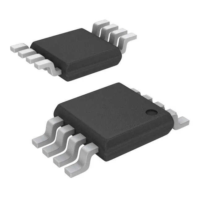
amplifier is packaged in a low cost, surface mount
8 leaded package with an exposed base for improved RF and thermal performance. The amplifier
provides 15 dB of gain, +29 dBm of saturated power
at 28% PAE from a +5V supply voltage. Power down
capability is available to conserve current consumption when the amplifier is not in use.
Electrical Specifications, TA = +25° C, Vs = 5V, Vpd = 5V
Parameter
Min.
Frequency Range
Gain
10
Gain Variation Over Temperature
Input Return Loss
Min.
21
15
18
0.025
0.035
Saturated Output Power (Psat)
25
12
32
Noise Figure
37
Max.
Units
GHz
15
18
dB
0.025
0.035
dB/ °C
12
dB
15
dB
22
25
dBm
29
dBm
36
40
dBm
29
Output Third Order Intercept (IP3)
Typ.
5.6 - 6.0
15
Output Power for 1 dB Compression (P1dB)
9-1
Max.
12
Output Return Loss
5.5
5.5
dB
0.002 / 230
0.002 / 230
mA
Vpd = 5V
7
7
mA
tON, tOFF
30
30
ns
Supply Current (Icq)
Vpd = 0V/5V
Control Current (Ipd)
Switching Speed
Typ.
5-7
Information
furnished
by Analog
is believed
to Analog
be accurate
and reliable.
However,
For price,Way,
delivery,
placeNorwood,
orders: Analog
Devices, Inc.,
For price,
delivery,
andDevices
to place
orders:
Devices,
Inc.,
One no
Technology
P.O. and
Boxto9106,
MA 02062-9106
responsibility is assumed by Analog Devices for its use, nor for any infringements of patents or other
One
Technology Way, P.O. Box 9106, Norwood, MA 02062-9106
Phone: 781-329-4700
• Order
online
at www.analog.com
rights of third parties that may result from its use. Specifications
subject to change without
notice.
No
Phone:
781-329-4700
•
Order
online
at
www.analog.com
license is granted by implication or otherwise under any patent
or patent rights
of Analog
Devices. 1-800-ANALOG-D
Application
Support:
Phone:
Application Support: Phone: 1-800-ANALOG-D
Trademarks and registered trademarks are the property of their respective owners.
�HMC407MS8G / 407MS8GE
v04.1019
GaAs InGaP HBT MMIC
POWER AMPLIFIER, 5 - 7 GHz
Broadband Gain & Return Loss
Gain vs. Temperature
20
20
15
16
5
S21
S11
S22
0
GAIN (dB)
RESPONSE (dB)
10
-5
12
-15
9
+25 C
+85 C
-40 C
8
-10
4
0
-25
2
3
4
5
6
7
8
9
4
10
4.5
5
Input Return Loss vs. Temperature
6.5
7
7.5
8
0
+25 C
+85 C
-40 C
-5
+25 C
+85 C
-40 C
-5
RETURN LOSS (dB)
RETURN LOSS (dB)
6
Output Return Loss vs. Temperature
0
-10
-15
-10
-15
-20
-25
-20
4
4.5
5
5.5
6
6.5
7
7.5
4
8
4.5
5
P1dB vs. Temperature
6
6.5
7
7.5
8
7
7.5
8
Psat vs. Temperature
34
30
30
Psat (dBm)
34
26
22
+25 C
+85 C
-40 C
18
5.5
FREQUENCY (GHz)
FREQUENCY (GHz)
P1dB (dBm)
5.5
FREQUENCY (GHz)
FREQUENCY (GHz)
AMPLIFIERS - LINEAR & POWER - SMT
-20
26
+25 C
+85 C
-40 C
22
18
14
14
4
4.5
5
5.5
6
6.5
FREQUENCY (GHz)
7
7.5
8
4
4.5
5
5.5
6
6.5
FREQUENCY (GHz)
For price, delivery, and to place orders: Analog Devices, Inc., One Technology Way, P.O. Box 9106, Norwood, MA 02062-9106
Phone: 781-329-4700 • Order online at www.analog.com
Application Support: Phone: 1-800-ANALOG-D
9-2
�HMC407MS8G / 407MS8GE
v04.1019
GaAs InGaP HBT MMIC
POWER AMPLIFIER, 5 - 7 GHz
Output IP3 vs. Temperature
44
25
39
20
34
IP3 (dBm)
30
15
10
+25 C
+85 C
-40 C
24
Pout (dBm)
Gain (dB)
PAE (%)
5
19
0
14
0
4
8
12
16
20
4
4.5
5
INPUT POWER (dBm)
6
6.5
7
7.5
8
Gain & Power vs. Supply Voltage
10
18
30
8
16
28
6
14
26
12
24
10
22
GAIN (dB)
NOISE FIGURE (dB)
Noise Figure vs. Temperature
4
+25C
+85C
-40C
2
0
20
8
5
5.5
6
6.5
7
4.75
FREQUENCY (GHz)
5
5.25
Vcc SUPPLY VOLTAGE (Vdc)
Reverse Isolation vs. Temperature
Power Down Isolation
0
0
-10
-10
ISOLATION (dB)
ISOLATION (dB)
5.5
FREQUENCY (GHz)
+25 C
+85 C
-40 C
-20
-30
-20
-30
-40
-50
-40
4
4.5
5
5.5
6
6.5
FREQUENCY (GHz)
9-3
29
P1dB, Psat (dBm)
AMPLIFIERS - LINEAR & POWER - SMT
9
Pout (dBm), GAIN (dB), PAE (%)
Power Compression @ 5.8 GHz
7
7.5
8
4
5
6
7
8
FREQUENCY (GHz)
For price, delivery, and to place orders: Analog Devices, Inc., One Technology Way, P.O. Box 9106, Norwood, MA 02062-9106
Phone: 781-329-4700 • Order online at www.analog.com
Application Support: Phone: 1-800-ANALOG-D
�HMC407MS8G / 407MS8GE
v04.1019
GaAs InGaP HBT MMIC
POWER AMPLIFIER, 5 - 7 GHz
Gain, Power & Quiescent
Supply Current vs. Vpd @ 5.8 GHz
Absolute Maximum Ratings
200
25
20
P1dB
Psat
Gain
150
15
Icq
100
10
50
5
0
3
3.5
4
4.5
Collector Bias Voltage (Vcc1, Vcc2)
+5.5 Vdc
Control Voltage (Vpd)
+5.5 Vdc
RF Input Power (RFIN)(Vs = Vpd = +5Vdc)
+20 dBm
Junction Temperature
150 °C
Continuous Pdiss (T = 85 °C)
(derate 31 mW/°C above 85 °C)
2W
Thermal Resistance
(junction to ground paddle)
32 °C/W
Storage Temperature
-65 to +150 °C
Operating Temperature
-40 to +85 °C
5
Vpd (Vdc)
ELECTROSTATIC SENSITIVE DEVICE
OBSERVE HANDLING PRECAUTIONS
8-Lead Mini Small Outline Package with Exposed Pad [MINI_SO_EP]
(RH-8-1)
Dimensions shown in millimeters
Outline Drawing
3.10
3.00
2.90
8
3.10
3.00
2.90
0.94
0.86
0.78
5
1
0.65
BSC
2.26
2.16
2.06
5.05
4.90
4.75
4
TOP VIEW
BOTTOM VIEW
1.95 BSC
1.10
MAX
SIDE VIEW
PKG-003371
0.13
MAX
COPLANARITY
0.10
1.83
1.73
1.63
EXPOSED
PAD
0.25 GAGE
PLANE
0.40
0.33
0.25
6°
0°
0.23
0.08
END VIEW
0.70
0.55
0.40
0.95
REF
08-02-2019-B
2.5
Icq (mA)
GAIN (dB), P1dB (dBm), Psat (dBm)
30
COMPLIANT TO JEDEC STANDARDS MO-187-AA-T
8-Lead Mini Small Outline Package with Exposed Pad [MINI_SO_EP]
(RH-8-1)
Dimensions shown in millimeters
Package Information
Part Number
Package Body Material
Lead Finish
MSL Rating
HMC407MS8G
Low Stress Injection Molded Plastic
Sn/Pb Solder
MSL1
[1]
HMC407MS8GE
RoHS-compliant Low Stress Injection Molded Plastic
100% matte Sn
MSL1
[2]
HMC407MS8GETR
RoHS-compliant Low Stress Injection Molded Plastic
100% matte Sn
MSL1
[2]
HMC407MS8GTR
Low Stress Injection Molded Plastic
Sn/Pb Solder
MSL1
[1]
104987HMC407MS8G
Eval Board
Package Marking [3]
9
AMPLIFIERS - LINEAR & POWER - SMT
250
H407
XXXX
H407
XXXX
H407
XXXX
H407
XXXX
[1] Max peak reflow temperature of 235 °C
[2] Max peak reflow temperature of 260 °C
[3] 4-Digit lot number XXXX
For price, delivery, and to place orders: Analog Devices, Inc., One Technology Way, P.O. Box 9106, Norwood, MA 02062-9106
Phone: 781-329-4700 • Order online at www.analog.com
Application Support: Phone: 1-800-ANALOG-D
9-4
�HMC407MS8G / 407MS8GE
v04.1019
GaAs InGaP HBT MMIC
POWER AMPLIFIER, 5 - 7 GHz
Pin Descriptions
Pin Number
Function
Description
1
Vcc1
Power supply voltage for the first amplifier stage. An external bypass capacitor
of 330 pF is required as shown in the application schematic.
2
Vpd
Power control pin. For maximum power, this pin should be connected to 5V. A
higher voltage is not recommended. For lower die current, this voltage can be
reduced.
3, 6, 7
GND
Ground: Backside of package has exposed metal ground slug that must be
connected to ground thru a short path. Vias under the device are required.
4
RFIN
This pin is AC coupled
and matched to 50 Ohms.
5
RFOUT
This pin is AC coupled
and matched to 50 Ohms.
8
Vcc2
Power supply voltage for the output amplifier stage. An external bypass
capacitor of 330 pF is required. This capacitor should be placed no more than
20 mils form package lead.
Interface Schematic
AMPLIFIERS - LINEAR & POWER - SMT
9
Application Circuit
Note 1: Vcc1 and Vcc2 may be connected to a common Vcc.
Note 2: C2 should be located < 0.020” from Pin 8 (Vcc2).
9-5
For price, delivery, and to place orders: Analog Devices, Inc., One Technology Way, P.O. Box 9106, Norwood, MA 02062-9106
Phone: 781-329-4700 • Order online at www.analog.com
Application Support: Phone: 1-800-ANALOG-D
�HMC407MS8G / 407MS8GE
v04.1019
GaAs InGaP HBT MMIC
POWER AMPLIFIER, 5 - 7 GHz
Evaluation PCB
List of Materials for Evaluation PCB 104987
Item
Description
J1 - J2
PCB Mount SMA RF Connector
J3
2 mm DC Header
C1 - C3
330 pF Capacitor, 0603 Pkg.
C4
2.2 µF Capacitor, Tantalum
U1
HMC407MS8G / HMC407MS8GE Amplifier
PCB [2]
104628 Eval Board
[1] Reference this number when ordering complete evaluation PCB
[2] Circuit Board Material: Roger 4350
[1]
The circuit board used in the final application should
use RF circuit design techniques. Signal lines should
have 50 Ohm impedance while the package ground
leads and exposed paddle should be connected
directly to the ground plane similar to that shown. A
sufficient number of via holes should be used to connect the top and bottom ground planes. The evaluation board should be mounted to an appropriate heat
sink. The evaluation circuit board shown is available
from Analog Devices, upon request.
For price, delivery, and to place orders: Analog Devices, Inc., One Technology Way, P.O. Box 9106, Norwood, MA 02062-9106
Phone: 781-329-4700 • Order online at www.analog.com
Application Support: Phone: 1-800-ANALOG-D
AMPLIFIERS - LINEAR & POWER - SMT
9
9-6
�