0.1 GHz to 13.0 GHz,0.5 dB LSB, 6-Bit,
GaAs Digital Attenuator
HMC424ACHIPS
Data Sheet
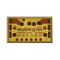
FUNCTIONAL BLOCK DIAGRAM
APPLICATIONS
Cellular infrastructure
Microwave radios and very small aperture terminals (VSATs)
Test equipment and sensors
Intermediate frequency (IF) and RF designs
Military and space
VEE
HMC424ACHIPS
RF1
1dB
2dB
4dB
8dB
16dB
RF2
0.5dB
Attenuation range: 0.5 dB (LSB) steps to 31.5 dB
±0.5 dB typical step error
Low insertion loss: 2.8 dB typical at 4.0 GHz
High linearity at VEE = −5 V
Input P0.1dB: 25 dBm typical
Input IP3: 45 dBm typical
High RF input power handling: 25 dBm maximum
Low relative phase: 30° at 6.0 GHz
Single-supply operation: −3 V to −5 V
Die size: 1.390 mm × 0.770 mm × 0.102 mm
V6
V5
V4
V3
V2
V1
13970-001
FEATURES
Figure 1.
GENERAL DESCRIPTION
The HMC424ACHIPS is a broadband, 6-bit, gallium arsenide
(GaAs), digital attenuator monolithic microwave integrated
circuit (MMIC) chip with a 31.5 dB attenuation control range in
0.5 dB steps.
The HMC424ACHIPS offers excellent attenuation accuracy of
±(0.2 dB + 3% of attenuation state) and high input linearity over
the specified frequency range from 0.1 GHz to 13.0 GHz with a
typical insertion loss of ≤4.2 dB. The attenuator bit values are
0.5 dB (LSB), 1 dB, 2 dB, 4 dB, 8 dB, and 16 dB for a total
attenuation of 31.5 dB with a ±0.5 dB of typical step error.
Rev. B
The device allows a user to program the attenuation state via six
parallel control inputs toggled between 0 V and VEE.
The HMC424ACHIPS operates with a single negative supply
voltage from −3 V to −5 V, and requires an external driver to
interface with a CMOS/transistor to transistor logic (TTL)
interface.
The HMC424ACHIPS comes in a RoHS compliant, 9-pad bare die.
Document Feedback
Information furnished by Analog Devices is believed to be accurate and reliable. However, no
responsibility is assumed by Analog Devices for its use, nor for any infringements of patents or other
rights of third parties that may result from its use. Specifications subject to change without notice. No
license is granted by implication or otherwise under any patent or patent rights of Analog Devices.
Trademarks and registered trademarks are the property of their respective owners.
One Technology Way, P.O. Box 9106, Norwood, MA 02062-9106, U.S.A.
Tel: 781.329.4700
©2020 Analog Devices, Inc. All rights reserved.
Technical Support
www.analog.com
�HMC424ACHIPS
Data Sheet
TABLE OF CONTENTS
Features .............................................................................................. 1
Applications ....................................................................................... 1
Insertion Loss, Return Loss, State Error, Step Error, and
Relative Phase ................................................................................6
Functional Block Diagram .............................................................. 1
Input Power Compression and Third-Order Intercept ............8
General Description ......................................................................... 1
Theory of Operation .........................................................................9
Revision History ............................................................................... 2
Power Supply..................................................................................9
Specifications..................................................................................... 3
RF Input and Output ....................................................................9
Absolute Maximum Ratings ............................................................ 4
Applications Information .............................................................. 10
Thermal Resistance ...................................................................... 4
Mounting and Bonding Techniques ........................................ 10
ESD Caution .................................................................................. 4
Assembly Diagram ..................................................................... 10
Pin Configuration and Function Descriptions ............................. 5
Outline Dimensions ....................................................................... 11
Interface Schematics..................................................................... 5
Ordering Guide .......................................................................... 11
Typical Performance Characteristics ............................................. 6
REVISION HISTORY
3/2020—Rev. 01.1115 to Rev. B
This Hittite Microwave Products data sheet has been reformatted to
meet the styles and standards of Analog Devices, Inc.
Changes to Title, Features Section, Applications Section, and
General Description Section ........................................................... 1
Changes to Table 1 ............................................................................ 3
Added Table 2, Figure 2, Thermal Resistance Section, and
Table 3; Renumbered Sequentially ................................................. 4
Changes to Table 2 ............................................................................ 4
Deleted Bias Voltage & Current Table and Control Voltage
Table; Renumbered Sequentially .................................................... 5
Added Figure 3, Table 4, and Figure 4 ........................................... 5
Changes to Figure 5 .......................................................................... 5
Added Insertion Loss, Return Loss, State Error, Step Error, and
Relative Phase Section, Figure 8, Figure 9, and Figure 12 ........... 6
Changes to Figure 7, Figure 10, and Figure 11 ............................. 6
Added Figure 13, Figure 14, and Figure 16 ................................... 7
Changes to Figure 15 ........................................................................ 7
Deleted Handling Precautions Section, Mounting Section, and
Wire Bonding Section .......................................................................7
Added Input Power Compression and Third-Order Intercept
Section, Figure 18 to Figure 20, and Figure 22 ..............................8
Changes to Figure 17 and Figure 21 ...............................................8
Added Theory of Operation Section, Power Supply Section, and
RF Input and Output Section...........................................................9
Changes to Figure 23.........................................................................9
Added Applications Information Section ................................... 10
Changed Mounting & Bonding Techniques for Millimeterwave
GaAs MMICs Section to Mounting and Bonding Techniques
Section .............................................................................................. 10
Changes to Mounting and Bonding Techniques Section,
Figure 24, and Figure 25 ................................................................ 10
Updated Outline Dimensions ....................................................... 11
Changes to Ordering Guide .......................................................... 11
Rev. B | Page 2 of 11
�Data Sheet
HMC424ACHIPS
SPECIFICATIONS
Supply voltage (VEE) = -3 V to -5 V, control input voltage (VCTL) = 0 V or VEE, TCASE = 25°C, 50 Ω system, unless otherwise noted.
Table 1.
Parameter
FREQUENCY RANGE
INSERTION LOSS
Symbol
Test Conditions/Comments
IL
0.1 GHz to 4.0 GHz
4.0 GHz to 8.0 GHz
8.0 GHz to 13.0 GHz
0.1 GHz to 13.0 GHz
Between minimum and
maximum attenuation states
Between any successive
attenuation states
Between any successive
attenuation states
All attenuation states,
referenced to insertion loss state
0.1 GHz to 8.0 GHz
ATTENUATION
Range
Step Size
Step Error
State Error
8.0 GHz to 13.0 GHz
RETURN LOSS (RF1 AND RF2)
RELATIVE PHASE
SWITCHING CHARACTERISTICS
Rise and Fall Time
On and Off Time
INPUT LINEARITY1
0.1 dB Compression
P0.1dB
Third-Order Intercept
IP3
SUPPLY CURRENT
DIGITAL CONTROL INPUTS
Voltage
Low
High
Current
Low
High
1
tRISE, tFALL
tON, tOFF
IDD
VINL
VINH
Min
0.1
2.8
3.4
4.2
0.5
dB
±0.5
dB
+(0.2 + 3% of
attenuation state)
+(0.2 + 4% of
attenuation state)
dB
dB
30
70
Degrees
Degrees
30
50
ns
ns
23
25
45
dBm
dBm
dBm
35
dBm
35
1
Rev. B | Page 3 of 11
dB
12
−1.0
−3.0
−3.0
−5.0
Input linearity performance degrades at frequencies less than 250 MHz; see Figure 17, Figure 21, and Figure 22.
Unit
GHz
dB
dB
dB
dB
2
IINL
IINH
Max
13.0
3.3
4.0
4.6
31.5
−(0.2 + 3% of
attenuation state)
−(0.2 + 4% of
attenuation state)
All attenuation states,
0.1 GHz to 13.0 GHz
Between minimum and
maximum attenuation states
0.1 GHz to 6.0 GHz
6.0 GHz to 13.0 GHz
Between all attenuation states
10% to 90% of RF output
50% VCTL to 90% of RF output
All attenuation states,
500 MHz to 6.0 GHz
VEE = −3 V
VEE = −5 V
VEE = −5 V, 10 dBm per tone,
1 MHz spacing
VEE = −3 V, 10 dBm per tone,
1 MHz spacing
VEE = −3 V to −5 V
V1 to V6
VEE = −3 V
VEE = −5 V
VEE = −3 V
VEE = −5 V
VEE = −3 V to −5 V
Typ
5
mA
0
0
−2.2
−4.2
V
V
V
V
μA
μA
�HMC424ACHIPS
Data Sheet
ABSOLUTE MAXIMUM RATINGS
THERMAL RESISTANCE
Table 2.
Parameter
Supply Voltage, VEE
Digital Control Input Voltage
RF Input Power1 (All Attenuation States,
f = 0.8 to 13.0 GHz, TCASE = 85°C,
VEE = −3 V to −5 V)
Continuous Power Dissipation, PDISS
(TCASE = 85°C)
Temperature
Junction, TJ
Storage
ESD Sensitivity, Human Body Model
(HBM)
1
Thermal performance is directly linked to printed circuit board
(PCB) design and operating environment. Careful attention to
PCB thermal design is required.
Rating
−7 V
VEE – 0.5 V
25 dBm
θJC is the junction to case thermal resistance.
Table 3. Thermal Resistance
0.56 W
Package Type
C-9-21
150°C
−65°C to +150°C
250 V (Class 1A)
1
ESD CAUTION
Stresses at or above those listed under Absolute Maximum
Ratings may cause permanent damage to the product. This is a
stress rating only; functional operation of the product at these
or any other conditions above those indicated in the operational
section of this specification is not implied. Operation beyond
the maximum operating conditions for extended periods may
affect product reliability.
Only one absolute maximum rating can be applied at any one
time.
0
–6
–8
–10
–12
0.10
1.00
FREQUENCY (GHz)
13970-026
POWER DERATING (dB)
VEE = –5V
VEE = –3V
–4
–14
0.01
Unit
°C/W
Thermal impedance simulated values are based on a JEDEC 2S2P thermal
test board with nine thermal vias. See JEDEC JESD51.
For power derating at frequencies less than 800 MHz, see Figure 2.
–2
θJC
330
Figure 2. Power Derating at Frequencies Less than 0.8 GHz
Rev. B | Page 4 of 11
�Data Sheet
HMC424ACHIPS
VEE
PIN CONFIGURATION AND FUNCTION DESCRIPTIONS
2
HMC424ACHIPS
6
5
4
V2
V1
V5
7
V3
8
V4
9
3
RF2
13970-002
TOP VIEW
(Not to Scale)
1
V6
RF1
Figure 3. Pin Configuration
Table 4. Pin Function Descriptions
Pad No.
1
Mnemonic
RF1
2
3
VEE
RF2
4 to 9
V1 to V6
Description
Attenuator RF Input. This pin is dc-coupled and ac matched to 50 Ω. An external dc blocking capacitor is required if
the RF line potential is not equal to 0 V.
Power Supply.
Attenuator RF Output. This pin is dc-coupled and ac matched to 50 Ω. An external dc blocking capacitor is
required if the RF line potential is not equal to 0 V.
Parallel Control Voltage Inputs. These pins select the required attenuation (see Table 5). There is an internal pulldown resistor on these pins to VEE.
VEE
3pF
13970-003
RF1, RF2
Figure 6. VEE Interface Schematic
100kΩ
VEE
13970-004
Figure 4. RF1 and RF2 Interface Schematic
V1 TO V6
2kΩ
13970-005
INTERFACE SCHEMATICS
Figure 5. V1 to V6 Interface Schematic
Rev. B | Page 5 of 11
�HMC424ACHIPS
Data Sheet
TYPICAL PERFORMANCE CHARACTERISTICS
INSERTION LOSS, RETURN LOSS, STATE ERROR, STEP ERROR, AND RELATIVE PHASE
0
0
–3
–4
–6
1
2
4
3
5
6
7
8
9
10 11
12 13 14
15
FREQUENCY (GHz)
–15
–20
Figure 7. Insertion Loss vs. Frequency over Temperature
2.0dB
16.0dB
1.0dB
8.0dB
–30
–35
0
1
2
3
4
5
6
7
8
9
10 11
12 13 14
15
FREQUENCY (GHz)
Figure 10. Normalized Attenuation vs. Frequency over Major Attenuation
States
0
0
–10
0.5dB
2.0dB
8.0dB
31.5dB
–10
OUTPUT RETURN LOSS (dB)
0dB
1.0dB
4.0dB
16.0dB
–5
INPUT RETURN LOSS (dB)
0.5dB
4.0dB
31.5dB
–25
13970-006
–5
–10
13970-009
–2
0
–5
–15
–20
–25
–30
–35
–40
–20
–30
–40
–50
0dB
1.0dB
4.0dB
16.0dB
–60
–45
0
1
2
3
4
5
6
7
8
9
10 11
12 13 14
15
FREQUENCY (GHz)
–70
13970-007
–50
Figure 8. Input Return Loss vs. Frequency over Major Attenuation States
0.5dB
2.0dB
8.0dB
31.5dB
0
1
2
3
4
5
6
7
8
9
10 11
12 13 14
15
FREQUENCY (GHz)
13970-010
INSERTION LOSS (dB)
–1
NORMALIZED ATTENUATION (dB)
TA = +85°C
TA = +25°C
TA = –40°C
Figure 11. Output Return Loss vs. Frequency over Major Attenuation States
2.0
2.0
0.1MHz
4.0GHz
8.0GHz
13.0GHz
1.5
1.5
STATE ERROR (dB)
1.0
0.5
0.5
0
–0.5
–1.0
0.5dB
2.0dB
8.0dB
31.5dB
–1.5
–0.5
0
2
4
6
8
10 12 14 16 18 20 22 24 26 28 30 32
ATTENUATION STATE (dB)
Figure 9. State Error vs. Attenuation State over Frequency
1.0dB
4.0dB
16.0dB
–2.0
0
1
2
3
4
5
6
7
8
9
10 11
12 13 14
15
FREQUENCY (GHz)
Figure 12. State Error vs. Frequency over Major Attenuation States
Rev. B | Page 6 of 11
13970-011
0
13970-008
STATE ERROR (dB)
1.0
�Data Sheet
HMC424ACHIPS
1.0
2.0
0.1MHz
4.0GHz
8.0GHz
13.0GHz
0.8
0.6
1.0dB
4.0dB
16.0dB
0.5dB
2.0dB
8.0dB
31.5dB
1.5
STEP ERROR (dB)
STEP ERROR (dB)
1.0
0.4
0.2
0
–0.2
0.5
0
–0.5
–0.4
–1.0
–0.6
0
2
4
6
8
10 12 14 16 18 20 22 24 26 28 30 32
ATTENUATION STATE (dB)
–2.0
13970-012
–1.0
0
2
3
4
5
6
7
8
9
10 11
12 13 14
15
FREQUENCY (GHz)
Figure 13. Step Error vs. Attenuation State over Frequency
Figure 15. Step Error vs. Frequency over Major Attenuation States
70
80
RELATIVE PHASE (Degrees)
50
40
30
20
10
60
50
40
30
20
10
0
–10
–10
2
4
6
8
10 12 14 16 18 20 22 24 26 28 30 32
ATTENUATION STATE (dB)
Figure 14. Relative Phase vs. Attenuation State over Frequency
13970-013
0
0
1.0dB
4.0dB
16.0dB
0.5dB
2.0dB
8.0dB
31.5dB
70
0
1
2
3
4
5
6
7
8
9
10 11
FREQUENCY (GHz)
12 13 14
15
13970-015
0.1MHz
4.0GHz
8.0GHz
13.0GHz
60
RELATIVE PHASE (Degrees)
1
13970-014
–1.5
–0.8
Figure 16. Relative Phase vs. Frequency over Major Attenuation States
Rev. B | Page 7 of 11
�HMC424ACHIPS
Data Sheet
INPUT POWER COMPRESSION AND THIRD-ORDER INTERCEPT
30
50
45
40
35
20
INPUT IP3 (dBm)
15
10
20
10
5
2
3
4
5
6
7
8
9
10 11
12 13 14
15
FREQUENCY (GHz)
0
25
50
20
40
INPUT IP3 (dBm)
60
0.5dB
2.0dB
8.0dB
31.5dB
0
0
1
2
3
4
5
6
7
8
9
10 11
12 13 14
15
FREQUENCY (GHz)
INPUT IP3 (dBm)
40
10
0.5dB
2.0dB
8.0dB
31.5dB
4
5
6
7
8
9
10 11
FREQUENCY (GHz)
12 13 14
15
15
1.0dB
4.0dB
16.0dB
IL
4
6
10
8
12
14
30
20
0.5dB
2.0dB
8.0dB
31.5dB
1.0dB
4.0dB
16.0dB
IL
0
13970-018
3
2
10
0
12 13 14
Figure 21. Input IP3 vs. Frequency over Major Attenuation States,
VEE = −5 V
20
15
10 11
FREQUENCY (GHz)
50
2
9
0.5dB
2.0dB
8.0dB
31.5dB
0
25
1
8
20
60
0
7
6
30
30
0dB
1.0dB
4.0dB
16.0dB
5
0
Figure 18. Input P0.1dB vs. Frequency over Major Attenuation States,
VEE = −5 V
5
4
10
13970-017
0dB
1.0dB
4.0dB
16.0dB
5
3
Figure 20. Input IP3 vs. Frequency at Minimum Attenuation State over
VEE = −5 V and VEE = −3 V
30
10
2
FREQUENCY (GHz)
Figure 17. Input P0.1dB vs. Frequency at Minimum Attenuation State over
VEE = −5 V and VEE = −3 V
15
1
13970-020
1
13970-016
0
VEE = –5V
VEE = –3V
0
13970-019
VEE = –5V
VEE = –3V
0
INPUT P0.1dB (dBm)
25
15
5
INPUT P0.1dB (dBm)
30
0
2
4
6
8
10
12
14
FREQUENCY (GHz)
Figure 19. Input P0.1dB vs. Frequency over Major Attenuation States,
VEE = −3 V
Figure 22. Input IP3 vs. Frequency over Major Attenuation States,
VEE = −3 V
Rev. B | Page 8 of 11
13970-021
INPUT P0.1dB (dBm)
25
�Data Sheet
HMC424ACHIPS
THEORY OF OPERATION
RF INPUT AND OUTPUT
The HMC424ACHIPS incorporates a 6-bit attenuator die that
offers an attenuation range of 31.5 dB in 0.5 dB steps. The
attenuation state is changed by the parallel control voltage
inputs (V1 to V6) directly (see Table 5).
The attenuator in the HMC424ACHIPS is bidirectional. The
RF1 and RF2 pins are interchangeable as the RF input and
output ports. The attenuator is internally matched to 50 Ω at
both the input and the output. Therefore, no external matching
components are required.
The HMC424ACHIPS allows the user to program the
attenuation state via six parallel control inputs toggled between
0 V and VEE. When interfacing with a TTL/CMOS interface, an
external level shifter is required. An example simple driver
using standard logic ICs provides fast switching while using
minimum dc current. The series resistance is recommended to
suppress unwanted RF signals at the input of the V1 to V6
control lines.
The RF input and output pins of the HMC424ACHIPS are
internally dc biased to 0 V. Therefore, they require external dc
blocking capacitors if the RF line potential is not equal to 0 V.
Select the value of these dc blocking capacitors based on the
minimum operating frequency. Use larger value capacitors to
extend the operation to lower frequencies.
POWER SUPPLY
VZ = 5.1V
IZT = 50µA
COMPENSATED
DEVICES
CD4689
The HMC424ACHIPS requires a single dc voltage applied to
the VEE pin. The ideal power-up sequence is as follows:
4.
TTL
OR
CMOS
Connect the ground reference.
Apply a supply voltage to the VEE pin.
Power up the digital control inputs. The relative order of
the digital control inputs is not important.
Apply an RF input signal to RF1.
VCC
10kΩ
GND
100Ω
74HCT04 (TTL)
OR 74HC04 (CMOS)
TO GaAs IC
ATTENUATOR
CONTROL INPUTS
V1 TO V6
–5V dc
NOTE
CD4689 IS A ZENER DIODE. VZ IS THE ZENER VOLTAGE, AND IZT
IS THE ZENER TEST CURRENT.
The power-down sequence is the reverse of the power-up
sequence.
Figure 23. Suggested Driver Circuit
Table 5. V1 to V6 Truth Table
V1 (16 dB)
Low
Low
Low
Low
Low
Low
High
High
1
V2 (8 dB)
Low
Low
Low
Low
Low
High
Low
High
Control Voltage Input
V3 (4 dB)
V4 (2 dB)
Low
Low
Low
Low
Low
Low
Low
High
High
Low
Low
Low
Low
Low
High
High
V5 (1 dB)
Low
Low
High
Low
Low
Low
Low
High
V6 (0.5 dB)
Low
High
Low
Low
Low
Low
Low
High
Attenuation State, RF1 to RF2
Reference insertion loss
0.5 dB
1 dB
2 dB
4 dB
8 dB
16 dB
31.5 dB
Any combination of the control voltage input states shown in Table 5 provides an attenuation equal to the sum of the bits selected.
Rev. B | Page 9 of 11
13970-022
1.
2.
3.
�HMC424ACHIPS
Data Sheet
APPLICATIONS INFORMATION
MOUNTING AND BONDING TECHNIQUES
The HMC424ACHIPS is back metallized and must be attached
directly to the ground plane with gold tin (AuSn) eutectic
preforms or with electrically conductive epoxy.
(4 mil) thick die to a 0.150 mm (6 mil) thick molybdenum heat
spreader (moly tab), which is then attached to the ground plane
(see Figure 25).
0.102mm (0.004") THICK GaAs MMIC
The die thickness is 0.102 mm (4 mil). The 50 Ω microstrip
transmission lines on 0.127 mm (5 mil) thick alumina thin film
substrates are recommended for bringing RF to and from the
HMC424ACHIPS (see Figure 24).
RIBBON BOND
0.076mm
(0.003")
0.102mm (0.004") THICK GaAs MMIC
0.150mm
(0.006”) THICK
MOLY TAB
RIBBON BOND
0.076mm
(0.003")
0.254mm (0.010") THICK ALUMINA
THIN FILM SUBSTRATE
13970-024
RF GROUND PLANE
Figure 25. Bonding RF Pads to 10 mil Substrate
Microstrip substrates are placed as close to the
HMC424ACHIPS as possible to minimize bond length. Typical
die to substrate spacing is 0.076 mm (3 mil).
Figure 24. Bonding RF Pads to 5 mil Substrate
When using 0.254 mm (10 mil) thick alumina thin film substrates,
the HMC424ACHIPS must be raised 0.150 mm (6 mil) so that the
surface of the HMC424ACHIPS is coplanar with the surface of the
substrate. One way to accomplish this is by attaching the 0.102 mm
50Ω
TRANSMISSION
LINE
RF bonds made with 3 mil × 5 mil ribbon are recommended.
DC bonds made with 1 mil diameter wire are recommended.
All bonds must be as short as possible.
ASSEMBLY DIAGRAM
An assembly diagram of the HMC424ACHIPS is shown in
Figure 26.
TO –5V SUPPLY
RF AND DC BONDS
1mm GOLD WIRE
Figure 26. Assembly Diagram
Rev. B | Page 10 of 11
3mm
NOMINAL
GAP
13970-025
0.127mm (0.005") THICK ALUMINA
THIN FILM SUBSTRATE
13970-023
RF GROUND PLANE
�Data Sheet
HMC424ACHIPS
OUTLINE DIMENSIONS
1.390
0.437
0.082
0.102
0.788
0.043
2
0.212
1
3
0.770
0.212
0.358
9
8
7
0.082
6
5
0.227
4
TOP VIEW
0.157
0.170
0.170
0.170
0.170
0.170
07-19-2019-A
SIDE VIEW
(CIRCUIT SIDE)
0.217
Figure 27. 9-Pad Bare Die [CHIP]
(C-9-2)
Dimensions shown in millimeters
ORDERING GUIDE
Model1
HMC424A
Temperature Range
−40°C to +85°C
Package Description
9-Pad Bare Die [CHIP]
Package Option
C-9-2
Marking Code2
HMC424A-SX
−40°C to +85°C
9-Pad Bare Die [CHIP]
C-9-2
H424A
XXXX
1
2
All models are RoHS compliant.
XXXX is the 4-digit lot number.
©2020 Analog Devices, Inc. All rights reserved. Trademarks and
registered trademarks are the property of their respective owners.
D13970-3/20(B)
Rev. B | Page 11 of 11
H424A
XXXX
�