HMC491LP3 / 491LP3E
v03.1206
Typical Applications
Features
The HMC491LP3 / HMC491LP3E is ideal for:
Gain: 16 dB
• Wireless Local Loop (WLL)
Noise Figure: 2 dB
• Fixed Wireless Access
Single Supply: +3V @ 9 mA
• Microwave & VSAT Radios
Integrated Bypass Mode
TE
50 Ohm Matched Input/Output
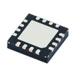
3 x 3 x 1 mm QFN SMT Package
Functional Diagram
General Description
LE
The HMC491LP3 & HMC491LP3E are versatile, integrated, Low Noise Amplifiers (LNA) featuring a bypass
mode intended for 3.4 to 3.8 GHz Fixed Wireless &
WLL applications. The amplifier provides 16 dB of
gain, 2 dB noise figure and +3 dBm input IP3 while
requiring only 9 mA from a +3V supply. Using a single
control line, the LNA can be switched into a low loss
2.2 dB bypass mode reducing the current consumption to 20 μA. A low cost, leadless 3x3 mm QFN surface mount package (LP3) houses the amplifier. No
external RF matching components are required.
B
SO
LOW NOISE AMPLIFIERS - SMT
8
GaAs MMIC LOW NOISE AMPLIFIER
w/ BYPASS MODE, 3.4 - 3.8 GHz
O
Electrical Specifi cations, TA = +25° C, Vdd = +3V
LNA Mode
LNA Mode
Bypass Mode
Parameter
Units
Min.
Frequency Range
Gain
Typ.
Max.
Min.
3.4 - 3.6
14.5
Gain Variation Over Temperature
Typ.
Max.
Min.
3.6 - 3.8
17
13
Typ.
Max.
3.4 - 3.8
15.5
-2.8
GHz
-2.3
dB
0.012
0.02
0.012
0.02
Noise Figure
2.2
2.7
2.0
2.5
Input Return Loss
12
17
18
dB
Output Return Loss
9
7
11
dB
Reverse Isolation
Input or Output Power for 1dB Compression (P1dB)*
34
3
6
33
4
7
25
0.004
0.008
dB / °C
--
--
dB
--
dB
28
dBm
Input Third Order Intercept (IP3)
(-20 dBm Input Power per tone, 1 MHz tone spacing)
1
3
11
dBm
Supply Current (Idd)
9
9
0.03
mA
* P1dB for LNA Mode is referenced to RFOUT while P1dB for Bypass Mode is referenced to RFIN.
8 - 126
For price,
delivery,
and to placeCorporation:
orders: Analog Devices, Inc.,
For price, delivery, and to place orders, please contact
Hittite
Microwave
One Technology Way, P.O. Box 9106, Norwood, MA 02062-9106
20 Alpha Road, Chelmsford, MA 01824 Phone: Phone:
978-250-3343
978-250-3373
781-329-4700Fax:
• Order
online at www.analog.com
Application Support: Phone: 1-800-ANALOG-D
Order On-line at www.hittite.com
Information furnished by Analog Devices is believed to be accurate and reliable. However, no
responsibility is assumed by Analog Devices for its use, nor for any infringements of patents or other
rights of third parties that may result from its use. Specifications subject to change without notice. No
license is granted by implication or otherwise under any patent or patent rights of Analog Devices.
Trademarks and registered trademarks are the property of their respective owners.
�HMC491LP3 / 491LP3E
v03.1206
GaAs MMIC LOW NOISE AMPLIFIER
w/ BYPASS MODE, 3.4 - 3.8 GHz
8
LNA Mode
Gain vs. Temperature
LNA Mode
Broadband Gain & Return Loss
15
18
S21
S11
S22
GAIN (dB)
5
0
-5
-15
3
3.2
3.4
3.6
3.8
10
3.4
4
B
SO
RETURN LOSS (dB)
3.8
3.5
3.6
3.7
-9
-12
-15
3.4
3.8
O
LNA Mode
Noise Figure vs. Temperature
3.5
3.6
3.7
3.8
FREQUENCY (GHz)
LNA Mode
Reverse Isolation vs. Temperature
5
0
+25 C
+85 C
-40 C
-10
ISOLATION (dB)
4
+25 C
+85 C
-40 C
-6
FREQUENCY (GHz)
NOISE FIGURE (dB)
3.7
LNA Mode
Output Return Loss vs. Temperature
-3
+25 C
+85 C
-40 C
-5
3
2
+25 C
+85 C
-40 C
-20
-30
1
0
3.4
3.6
0
0
-20
3.4
3.5
LE
LNA Mode
Input Return Loss vs. Temperature
-15
+25 C
+85 C
-40 C
FREQUENCY (GHz)
FREQUENCY (GHz)
-10
14
12
-20
-25
2.8
16
TE
-10
RETURN LOSS (dB)
RESPONSE (dB)
10
LOW NOISE AMPLIFIERS - SMT
20
20
3.5
3.6
3.7
3.8
FREQUENCY (GHz)
-40
3.4
3.5
3.6
3.7
3.8
FREQUENCY (GHz)
For price,
delivery,
and to placeCorporation:
orders: Analog Devices, Inc.,
For price, delivery, and to place orders, please contact
Hittite
Microwave
One Technology Way, P.O. Box 9106, Norwood, MA 02062-9106
20 Alpha Road, Chelmsford, MA 01824 Phone: Phone:
978-250-3343
978-250-3373
781-329-4700Fax:
• Order
online at www.analog.com
Application Support: Phone: 1-800-ANALOG-D
Order On-line at www.hittite.com
Information furnished by Analog Devices is believed to be accurate and reliable. However, no
responsibility is assumed by Analog Devices for its use, nor for any infringements of patents or other
rights of third parties that may result from its use. Specifications subject to change without notice. No
license is granted by implication or otherwise under any patent or patent rights of Analog Devices.
Trademarks and registered trademarks are the property of their respective owners.
8 - 127
�HMC491LP3 / 491LP3E
v03.1206
LNA Mode
Psat vs. Temperature
12
12
10
10
8
8
Psat (dBm)
6
+25 C
+85 C
-40 C
4
6
+25 C
+85 C
-40 C
4
TE
OUTPUT P1dB (dBm)
LNA Mode
Output P1dB vs. Temperature
2
2
0
3.4
3.5
3.6
3.7
0
3.4
3.8
3.5
LNA Mode
Input IP3 vs. Temperature
3.7
12
22
Noise Figure
Idd
4
10
8
-4
3.4
GAIN (dB)
0
B
SO
IP3 (dBm)
18
2
6
14
Gain
+25 C
+85 C
-40 C
3.5
3.6
3.7
0
10
3.8
2.7
2.8
2.9
-5
-1
INSERTION LOSS (dB)
RESPONSE (dB)
0
-10
-15
S21
S11
S22
3
3.2
3.6
3.8
3.2
3.3
-2
-3
+25 C
+85 C
-40 C
-4
3.4
3.1
Vdd (Vdc)
0
-25
2.8
3
Bypass Mode
Insertion Loss vs. Temperature
O
Bypass Mode
Broadband Insertion Loss & Return Loss
4
2
FREQUENCY (GHz)
-20
3.8
LNA Mode Gain, Noise Figure & Supply
Current vs. Supply Voltage @ 3.6 GHz
6
-2
4
FREQUENCY (GHz)
8 - 128
3.6
FREQUENCY (GHz)
LE
FREQUENCY (GHz)
NOISE FIGURE (dB), Idd (mA)
LOW NOISE AMPLIFIERS - SMT
8
GaAs MMIC LOW NOISE AMPLIFIER
w/ BYPASS MODE, 3.4 - 3.8 GHz
-5
3.4
3.5
3.6
3.7
3.8
FREQUENCY (GHz)
For price,
delivery,
and to placeCorporation:
orders: Analog Devices, Inc.,
For price, delivery, and to place orders, please contact
Hittite
Microwave
One Technology Way, P.O. Box 9106, Norwood, MA 02062-9106
20 Alpha Road, Chelmsford, MA 01824 Phone: Phone:
978-250-3343
978-250-3373
781-329-4700Fax:
• Order
online at www.analog.com
Application Support: Phone: 1-800-ANALOG-D
Order On-line at www.hittite.com
Information furnished by Analog Devices is believed to be accurate and reliable. However, no
responsibility is assumed by Analog Devices for its use, nor for any infringements of patents or other
rights of third parties that may result from its use. Specifications subject to change without notice. No
license is granted by implication or otherwise under any patent or patent rights of Analog Devices.
Trademarks and registered trademarks are the property of their respective owners.
�HMC491LP3 / 491LP3E
v03.1206
GaAs MMIC LOW NOISE AMPLIFIER
w/ BYPASS MODE, 3.4 - 3.8 GHz
0
+25 C
+85 C
-40 C
RETURN LOSS (dB)
-20
3.5
3.6
3.7
-15
3.4
3.8
3.7
3.8
3.7
3.8
LE
30
28
B
SO
16
IP3 (dBm)
3.6
Bypass Mode
Input P1dB vs. Temperature
20
0
3.4
3.5
FREQUENCY (GHz)
Bypass Mode
Input IP3 vs. Temperature
4
-9
-12
FREQUENCY (GHz)
8
-6
TE
-15
+25 C
+85 C
-40 C
3.5
3.6
3.7
3.8
INPUT P1dB (dBm)
RETURN LOSS (dB)
-10
12
+25 C
+85 C
-40 C
-3
26
+25 C
+85 C
-40 C
24
22
20
3.4
3.5
FREQUENCY (GHz)
O
Absolute Maximum Ratings
Drain Bias Voltage (Vdd)
RF Input Power (RFIN)
(Vdd = +3.0 Vdc)
LNA Mode
Bypass Mode
Vdd (Vdc)
0 dBm
+30 dBm
150 °C
Continuous Pdiss (T = 85 °C)
(derate 1.8 mW/°C above 85 °C)
0.117 W
Thermal Resistance
(channel to ground paddle)
556 °C/W
Storage Temperature
-65 to +150 °C
Operating Temperature
-40 to +85 °C
3.6
FREQUENCY (GHz)
Typical Supply Current vs. Vdd
+7.0 Vdc
Channel Temperature
LOW NOISE AMPLIFIERS - SMT
0
-5
-25
3.4
8
Bypass Mode
Output Return Loss vs. Temperature
Bypass Mode
Input Return Loss vs. Temperature
Idd (mA)
+2.7
7.6
+3.0
9.0
+3.3
10.2
Truth Table
LNA Mode
Vctl= Vdd @ 1.6 mA
Bypass Mode
Vctl= 0Vdc @ -13 µA
Vdd= +3V ±10%
ELECTROSTATIC SENSITIVE DEVICE
OBSERVE HANDLING PRECAUTIONS
For price,
delivery,
and to placeCorporation:
orders: Analog Devices, Inc.,
For price, delivery, and to place orders, please contact
Hittite
Microwave
One Technology Way, P.O. Box 9106, Norwood, MA 02062-9106
20 Alpha Road, Chelmsford, MA 01824 Phone: Phone:
978-250-3343
978-250-3373
781-329-4700Fax:
• Order
online at www.analog.com
Application Support: Phone: 1-800-ANALOG-D
Order On-line at www.hittite.com
Information furnished by Analog Devices is believed to be accurate and reliable. However, no
responsibility is assumed by Analog Devices for its use, nor for any infringements of patents or other
rights of third parties that may result from its use. Specifications subject to change without notice. No
license is granted by implication or otherwise under any patent or patent rights of Analog Devices.
Trademarks and registered trademarks are the property of their respective owners.
8 - 129
�HMC491LP3 / 491LP3E
v03.1206
GaAs MMIC LOW NOISE AMPLIFIER
w/ BYPASS MODE, 3.4 - 3.8 GHz
LE
TE
Outline Drawing
NOTES:
1. LEADFRAME MATERIAL: COPPER ALLOY
2. DIMENSIONS ARE IN INCHES [MILLIMETERS]
3. LEAD SPACING TOLERANCE IS NON-CUMULATIVE
4. PAD BURR LENGTH SHALL BE 0.15mm MAXIMUM.
PAD BURR HEIGHT SHALL BE 0.05mm MAXIMUM.
5. PACKAGE WARP SHALL NOT EXCEED 0.05mm.
6. ALL GROUND LEADS AND GROUND PADDLE MUST BE SOLDERED TO PCB RF GROUND.
7. REFER TO HITTITE APPLICATION NOTE FOR SUGGESTED LAND PATTERN.
B
SO
LOW NOISE AMPLIFIERS - SMT
8
Package Information
Part Number
Package Body Material
Lead Finish
MSL Rating
HMC491LP3
Low Stress Injection Molded Plastic
Sn/Pb Solder
MSL1
HMC491LP3E
RoHS-compliant Low Stress Injection Molded Plastic
100% matte Sn
MSL1
Package Marking [3]
[1]
491
XXXX
[2]
491
XXXX
[1] Max peak reflow temperature of 235 °C
[2] Max peak reflow temperature of 260 °C
[3] 4-Digit lot number XXXX
O
Pin Descriptions
Pin Number
8 - 130
Function
Description
1, 5 - 8, 12, 13
N/C
No connection necessary.
These pins may be connected to RF/DC ground.
2, 4, 9, 11, 15
GND
These pins must be connected to RF/DC ground.
3
RF IN
This pin is AC coupled and matched to 50 Ohms.
10
RF OUT
This pin is AC coupled and matched to 50 Ohms.
14
Vdd
Power supply voltage.
16
Vctl
Control voltage. Vctl= Vdd for LNA mode.
Vctl= 0V for bypass mode.
Interface Schematic
For price,
delivery,
and to placeCorporation:
orders: Analog Devices, Inc.,
For price, delivery, and to place orders, please contact
Hittite
Microwave
One Technology Way, P.O. Box 9106, Norwood, MA 02062-9106
20 Alpha Road, Chelmsford, MA 01824 Phone: Phone:
978-250-3343
978-250-3373
781-329-4700Fax:
• Order
online at www.analog.com
Application Support: Phone: 1-800-ANALOG-D
Order On-line at www.hittite.com
Information furnished by Analog Devices is believed to be accurate and reliable. However, no
responsibility is assumed by Analog Devices for its use, nor for any infringements of patents or other
rights of third parties that may result from its use. Specifications subject to change without notice. No
license is granted by implication or otherwise under any patent or patent rights of Analog Devices.
Trademarks and registered trademarks are the property of their respective owners.
�HMC491LP3 / 491LP3E
v03.1206
GaAs MMIC LOW NOISE AMPLIFIER
w/ BYPASS MODE, 3.4 - 3.8 GHz
TE
LE
B
SO
LOW NOISE AMPLIFIERS - SMT
8
Evaluation PCB
O
List of Materials for Evaluation PCB 107174 [1]
Item
Description
J1 - J2
PCB Mount SMA RF Connector
J3 - J6
DC Pin
U1
HMC491LP3 / HMC491LP3E Amplifier
PCB [2]
107431 Evaluation PCB
[1] Reference this number when ordering complete evaluation PCB
[2] Circuit Board Material: Rogers 4350
The circuit board used in the final application should
use RF circuit design techniques. Signal lines
should have 50 ohm impedance while the package
ground leads and exposed paddle should be connected directly to the ground plane similar to that
shown. A sufficient number of via holes should be
used to connect the top and bottom ground planes.
The evaluation circuit board shown is available from
Hittite upon request.
For price,
delivery,
and to placeCorporation:
orders: Analog Devices, Inc.,
For price, delivery, and to place orders, please contact
Hittite
Microwave
One Technology Way, P.O. Box 9106, Norwood, MA 02062-9106
20 Alpha Road, Chelmsford, MA 01824 Phone: Phone:
978-250-3343
978-250-3373
781-329-4700Fax:
• Order
online at www.analog.com
Application Support: Phone: 1-800-ANALOG-D
Order On-line at www.hittite.com
Information furnished by Analog Devices is believed to be accurate and reliable. However, no
responsibility is assumed by Analog Devices for its use, nor for any infringements of patents or other
rights of third parties that may result from its use. Specifications subject to change without notice. No
license is granted by implication or otherwise under any patent or patent rights of Analog Devices.
Trademarks and registered trademarks are the property of their respective owners.
8 - 131
�